

SGS Thomson Microelectronics M95040, M95020-W, M95020-R, M95020, M95010-W Datasheet
...
4/2/1 Kbit Serial SPI Bus EEPROM
■ Compatible with SPI Bus Serial Interface
(Positive Clock SPI Modes)
■ Single Supply Voltage:
– 4.5V to 5.5V for M950x0
– 2.5V to 5.5V for M950x0-W
– 1.8V to 3.6V for M950x0-R
■ 5 MHz Clock Rate (maximum)
■ Status Register
■ BYTE and PAGE WRITE (up to 16 Bytes)
■ Self-Tim ed P ro gr a m ming Cycle
■ Adjustable Size Read-Only EEPR OM Area
■ Enhanced ESD Protection
■ More than 1,000,000 Erase/Write Cycles
■ More than 40 Year Data Retention
DESCRIPTION
These SPI-compatible electrically erasable
programmable memory (EEPROM) devices are
organized as 512 x 8 bits, 256 x 8 bits and 128 x 8
bits (M95040, M95020, M95010). They operate
down to 2.5 V (for the -W version of each device),
and down to 1.8 V (for the -R version of each
device).
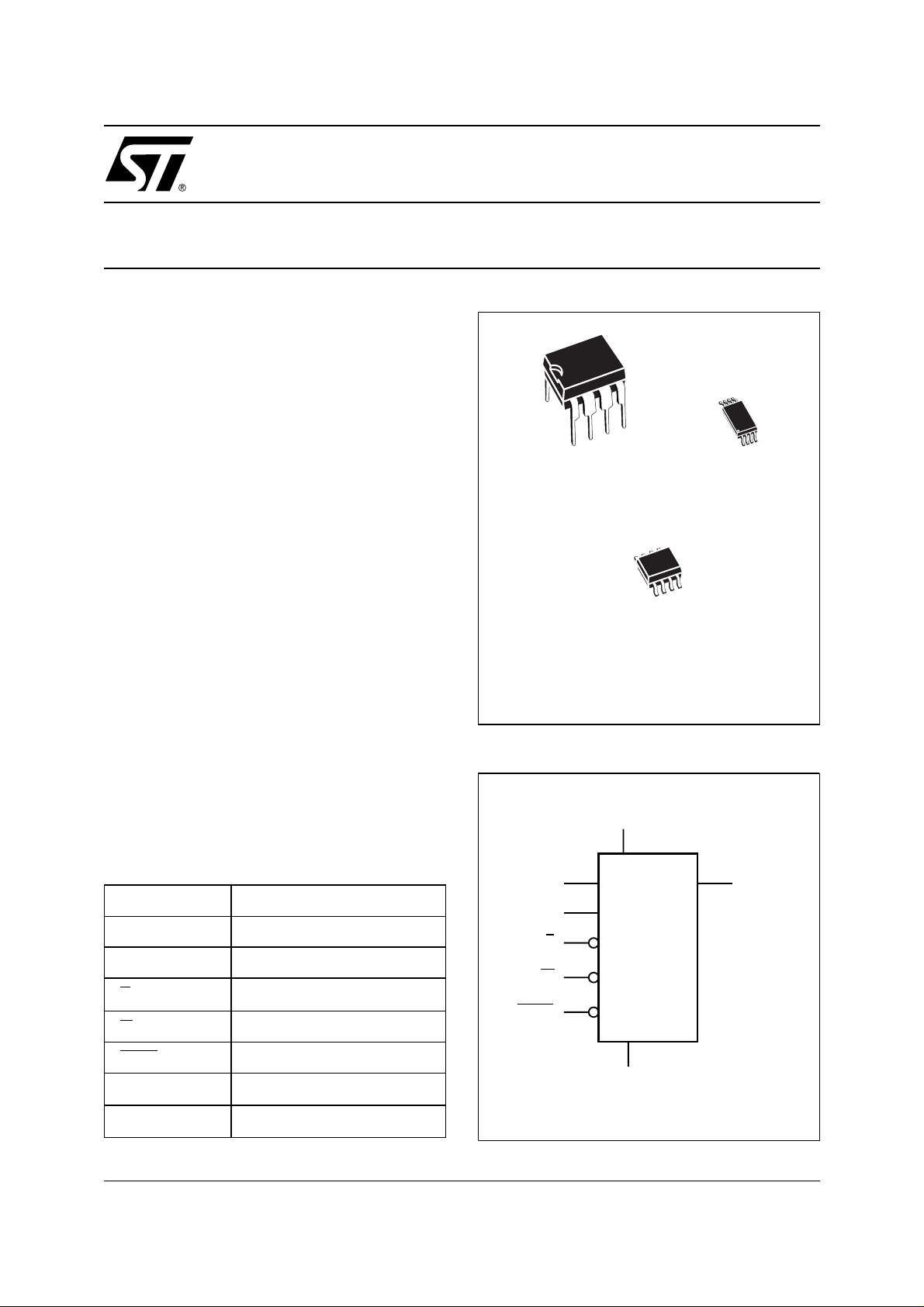
M95020, M95010
With High Speed Clock
8
1
PSDIP8 (BN)
0.25 mm frame
8
SO8 (MN)
150 mil width
Figure 1. Logic Diagram
M95040
PRELIMINARY DATA
8
1
TSSOP8 (DW)
169 mil width
1
V
CC
Table 1. Signal Names
C Serial Clock
D Serial Data Input
Q Serial Data Output
S
W
Write Protect
Hold
HOLD
V
CC
V
SS
May 2000
This is preliminary information on a new product now in development or undergoing evaluation. Details are subject to change without notice.
Chip Select
Supply Voltage
Ground
W
HOLD
D
C
S
M95xxx
V
SS
Q
AI01789C
1/19
M95040, M95020, M95010
Figure 2A. DIP Connections
M95xxx
1
SV
2
3
W
4
SS
8
7
6
5
AI01790C
CC
HOLDQ
C
DV
The M95040 and M95020, M95010 are available
in Plastic Dual-in-Line, Plastic Small Out line and
Thin Shrink Small Outline packages.
Each memory device is accessed by a simple
serial interface that is SPI-compatible. The bus
signals are C, D and Q, as shown in Table 1 and
Figure 3.
The device is selected when t he chip s elect input
) is held low. Communications with the chip can
(S
be interrupted using the hold input (HOLD
). Write
operations are disabled by the w rite protect input
(W
).
Figure 2B. SO and TSSOP Connections
M95xxx
1
SV
2
3
W
SS
4
8
7
6
5
AI01791C
CC
HOLDQ
C
DV
SIGNAL DESCRIPTION
Seria l O utput ( Q )
The output pin is used to transfer data serially out
of the Memory. Data is shifted out on the falling
edge of the serial clock.
Serial Inpu t ( D )
The input pin is used to transfer data serially into
the device. Instructions, addresses, and the data
to be written, are each received t his way. Input is
latched on the rising edge of the serial clock.
Serial Clock (C)
The serial clock provides the timing for the serial
interface (as shown in Figure 4). Instructions,
addresses, or data are latched, from the input pin,
Table 2. Absolute Maximum Ratings
Symbol Parameter Value Unit
T
A
T
STG
T
LEAD
V
O
V
I
V
CC
V
ESD
Note: 1. Exc ept for the rating “Operating Temperature Ra nge”, stres ses above those listed in the Table “Absolute Maximum Ratings” may
2/19
cause permanent damage to the device. These are stress ratings only, and operation of the device at these or any other conditions
above those indi cated in t he Operating sect i ons of thi s specifi cation i s not impl i ed. Exposure to Absolute M aximum Rating c onditions for extended periods may affect device reliability. Refer also to the ST SURE Program and other relevant quality documents.
2. MIL -STD-883C, 3015.7 (1 00 pF, 1500 Ω)
3. EIA J I C-121 (Condition C) (200pF, 0W).
Ambient Operating Temperature -40 to 125 °C
Storage Temperature -65 to 150 °C
Lead Temperature during Soldering
Output Voltage Range
Input Voltage Range -0.3 to 6.5 V
Supply Voltage Range -0.3 to 6.5 V
Electrostatic Discharge Voltage (Human Body model)
Electrostatic Discharge Voltage (Machine model)
1
PSDIP8: 10 sec
SO8: 40 sec
TSSOP8: t.b.c.
2
3
260
215
t.b.c.
-0.3 to V
+0.6
CC
4000 V
400 V
°C
V
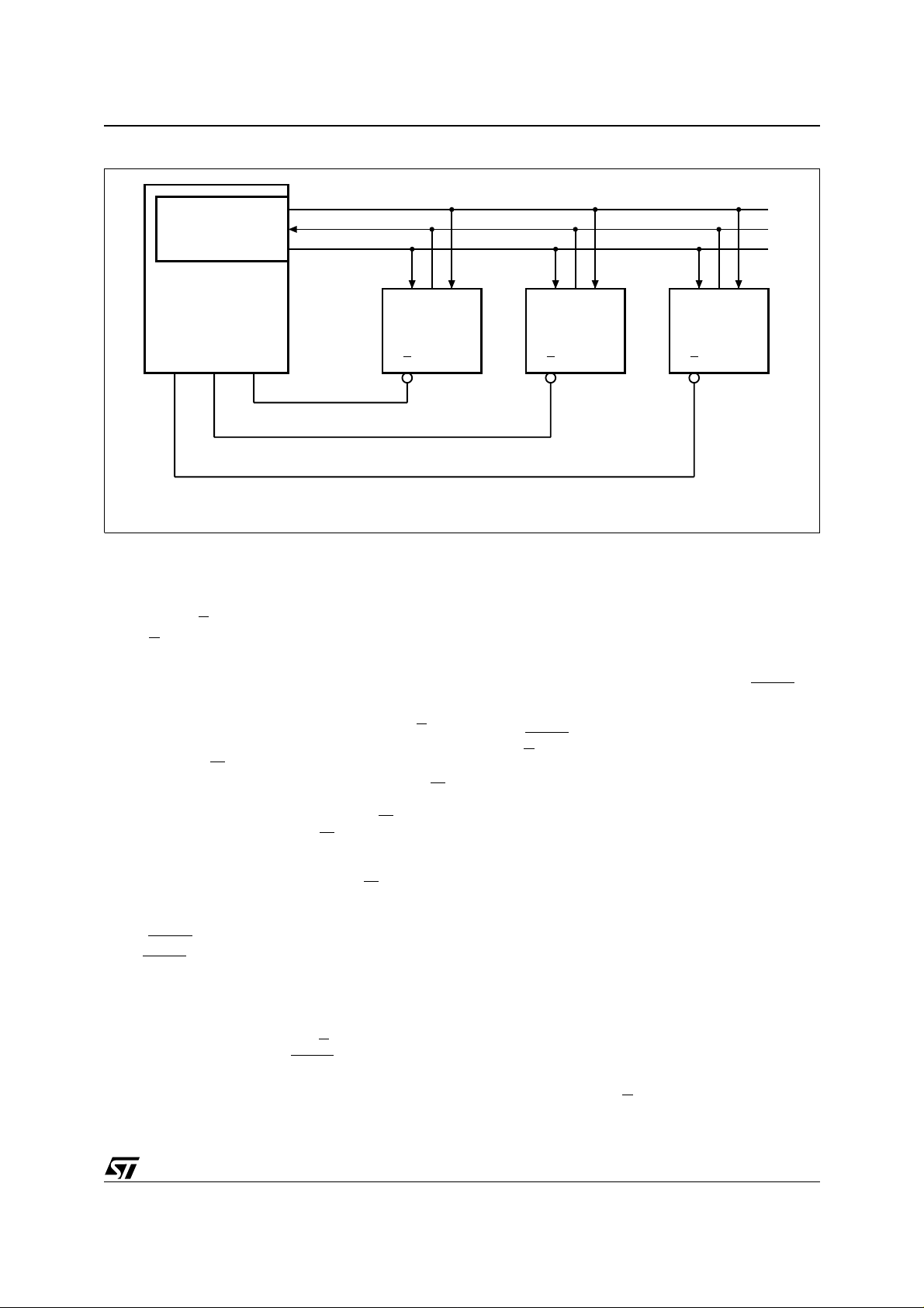
Figure 3. Microcontroller and Memor y Devices on the SPI Bus
M95040, M95020, M95010
SPI Interface with
(CPOL, CPHA) =
('0', '0') or ('1', '1')
Master
(ST6, ST7, ST9,
ST10, Others)
CS3 CS2 CS1
SDO
SDI
SCK
CQD
M95xxx
S
on the rising edge of the clock input. The output
data on the Q pin chang es state after the falling
edge of the clock input.
Chip Select (S
When S
is high, the memory device is deselected,
)
and the Q output pin is held in its high impe dance
state. Unless an internal write operation is
underway, the memory device is placed in its
stand-by power mode.
After power-on, a high-to-low transition on S
is
required prior to the start of any operation.
Write Protect (W
)
This pin is for hardware write protection. When W
is low, writes to the device are disabled, but all
other operations remain enabled. When W
write operations are enabled. If W
goes low at any
is high,
time before the last bit, D0, of the data stream, the
write enable latch is reset, thus preventing the
write from taking e ffect. No action on W
or on the
write enable latch can interrupt a write cycle which
has commenced, though.
Hold (HOLD
The HOLD
)
pin is used to pause the serial
communications between the SPI memory and
controller, without losing bits that have already
been decoded in the serial sequence. For a hold
condition to occur, the memory device must
already have been selected (S
condition starts when the HOLD
= 0). The hold
pin is held low
while the clock pin (C) is also low (as shown in
Figure 14).
CQD
M95xxx
S
CQD
M95xxx
S
AI01958C
During the hold condition, the Q output pin i s held
in its high impedance sta te, and the level s on the
input pins (D and C) are ignored by the memory
device.
It is possible to deselect the device whe n it is still
in the hold state, thereby resetting whatever
transfer had been in progress. The memory
remains in the hold state as long as the HOLD
pin
is low. To restart communication with the device, it
is necessary both to remove the hold condition (by
takin g HO LD
taking S
high) and to select the memory (by
low).
The Memory can be driven by a microcontroller
with its SPI periphe ral running in ei the r of the two
following modes: (CPOL, CPHA) = (’0’,’0’) or
(CPOL,CPHA) = (’1’,’1’).
For these two modes , input data is latched in by
the low to high transition of clock C, and output
data is available from the h igh to low t ransition of
Clock (C).
The difference between (CPOL, CPHA) = (0, 0)
and (CPOL, CPHA) = (1, 1) is the stand-by
polarity: C remains at ’0’ for (CPOL, CPHA) = (0,
0) and C remains at ’1’ for (CPOL, CPHA) = (1, 1)
when there is no data transfer.
OPERATIONS
All instructions, addresses and data are shifted
serially in and out of the chip. The most significant
bit is presented first, with the data input (D)
sampled on the first rising edge of the clock (C)
after the chip select (S
) goes low.
3/19
M95040, M95020, M95010
Figure 4. Dat a and Clock Timi ng
CPOL
CPHA
0
1
0
1
C
C
D or Q
MSB LSB
Every instruction starts with a single-byte code, as
summarized in Table 3. This code is entered via
the data input (D), and latched on the rising edge
of the clock input (C). To enter an instruction code,
the product must have been previously selected (S
held low). If an invalid i nstruction is sent (one not
contained in Table 3), the chip automatically
deselects itself.
Write Enable (WREN) and Write Disable (WRDI)
The write enable latch, inside the memory device,
must be set prior to each WRITE and WRSR
operation. The WREN instruction (write enable)
sets this latch, and the WRDI instruction (write
disable) resets it.
Table 3. Instruction Set
Instruc
tion
WREN Set Write Enable Latch 0000 X110
WRDI Reset Write Enable Latch 0000 X100
RDSR Read Status Register 0000 X101
WRSR Write Status Register 0000 X001
READ
WRITE Write Data to Memory Array
Note: 1 . A8 = 1 for the uppe r p age on th e M95 04 0, and 0 for the
Read Data from Memory
Array
lower page, and is Don’ t Care for othe r devices.
2. X = Don’t Care.
Description
Instruction
Format
8
8
011
010
0000 A
0000 A
Table 4. Status Register Format
b7 b0
1 1 1 1 BP1 BP0 WEL WIP
Note: 1. BP1 and BP0 are rea d and write bits.
2. WEL and WIP are read only bits.
3. b7 to b4 are read onl y bits.
AI01438
The latch becomes reset by any of the following
events:
– Power on
– WRDI instruction completion
– WRSR in s t ru ctio n completio n
– WRITE instruct ion c ompletion
– the W
pin is held low.
As soon as the WREN or WRDI instruction is
received, the memory device first executes the
instruction, then enters a wait mode until the
device is deselected.
Read Status Register (RDSR)
The RDSR instruction allows the status register to
be read, and can be sent at any time, even during
a Write operation. Indeed, when a Write is in
progress, it is recommended th at the value of t he
Write-In-Progress (WIP) bit be checked. The value
in the WIP bit (whose position in the status register
is shown in Table 4) can be polled, before sending
a new WRITE instruction.
The Write-In-Process (WIP) bit is read-only, and
indicates whether the memory is busy with a Write
operation. A ’1’ indicates that a write is in progress,
and a ’0’ that no write is in progress.
The Write Enable Latch (WEL) bit indicates the
status of the write enable latch. It, too, is read-only.
Its value can only be changed by one of the events
listed in the previous paragraph, or as a result of
executing WREN or WRDI instruction. It cannot be
changed using a WRSR instruction. A ’1’ indicates
that the latch is set (the forthcoming Write
instruction will be executed), and a ’0’ that it is
reset (and any forthcoming Write instructions will
be ignored).
The Block Protect (BP0 and BP1) bits indicate the
amount of the memory that is to be writeprotected. These two bits are non-volatile. They
are set using a WRSR instruction.
4/19
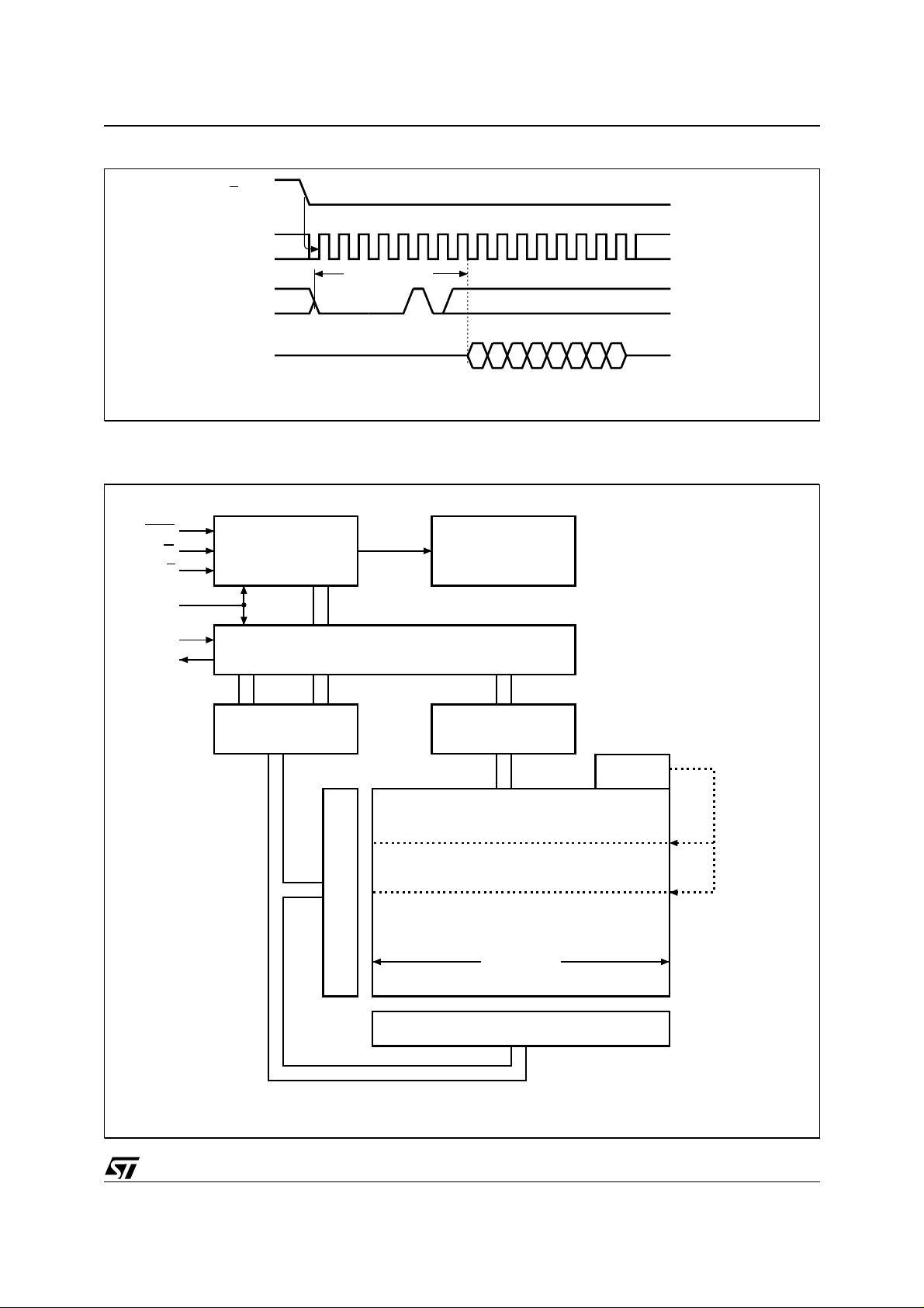
Figure 5. RDSR: Read Status Register Sequence
S
21 3456789101112131415
0
C
INSTRUCTION
D
M95040, M95020, M95010
Q
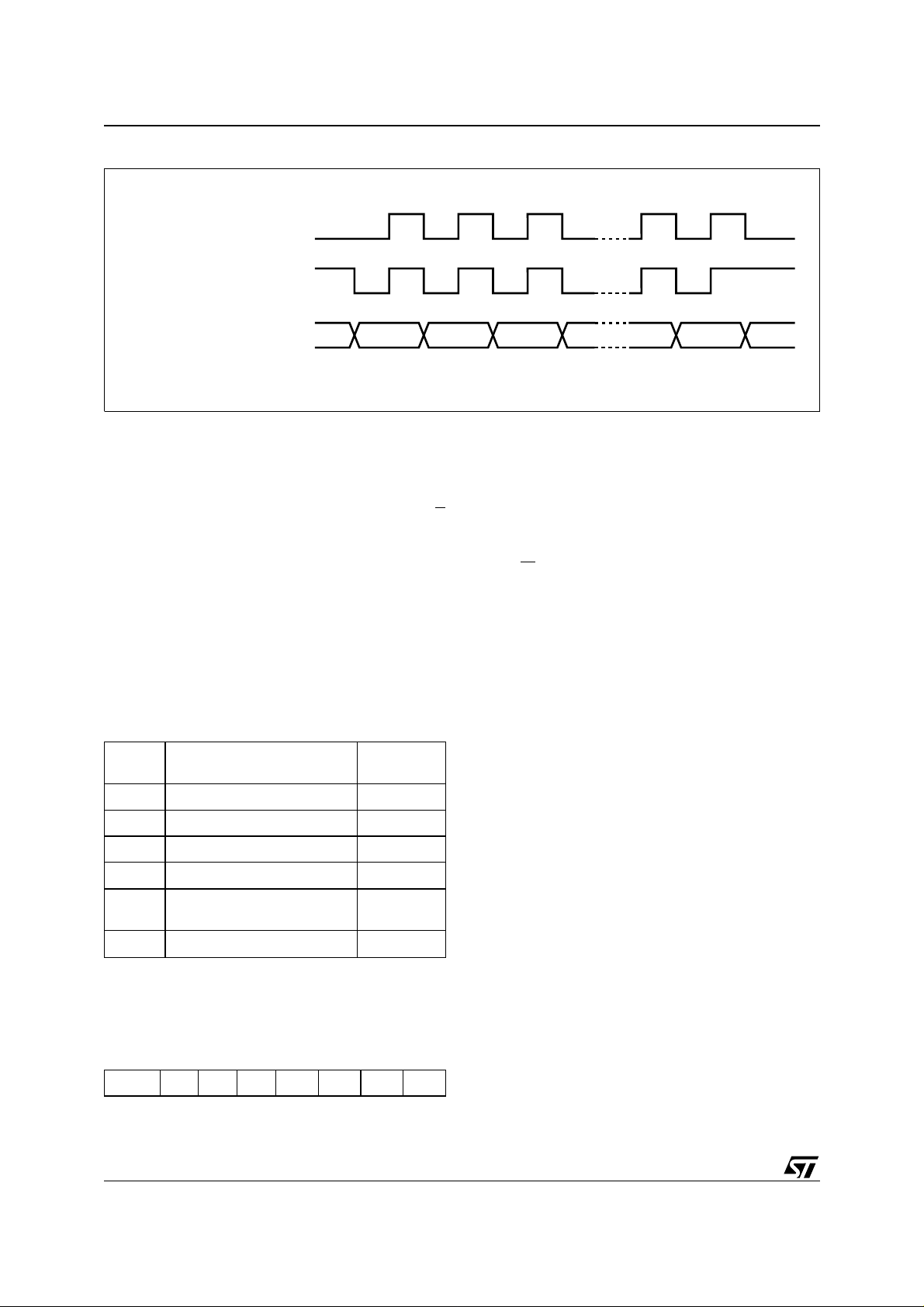
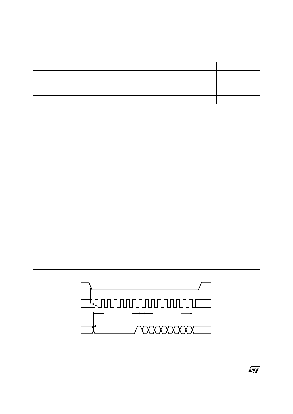
Figure 6. Block Diagram
HOLD
W
S
C
D
Q
Control Logic
Address Register
and Counter
HIGH IMPEDANCE
I/O Shift Register
STATUS REG. OUT
7 6543210
MSB
High Voltage
Generator
Data
Register
AI01444
Status
Register
Size of the
Read only
EEPROM
area
Y Decoder
16 Bytes
X Decoder
AI01272B
5/19
M95040, M95020, M95010
Table 5. Write Protected Block Size
Status Register Bits
Protected Block
BP1 BP0 M95040 M95020 M95010
0 0 none none none none
0 1 Upper quarter 180h - 1FFh C0h - FFh 060h - 7Fh
1 0 Upper half 100h - 1FFh 80h - FFh 040h - 7Fh
1 1 Whole memory 000h - 1FFh 00h - FFh 000h - 7Fh
Array Addresses Protected
During a Write operation (whether it be to the
memory area or to the status register), all bits of
the status register remain valid, and can be read
using the RDSR instruction. However, during a
Write operation, the values of the no n-vo latile bits
(BP0, BP1) become frozen at a constant value.
The updated value of these bits becomes
available when a new RDSR instruction is
executed, after completion of t he write cycle. On
the other hand, the two read-only bits (WEL, WIP)
are dynamically updated during internal write
cycles. U sing th is fac ility, it is possib le to p oll the
WIP bit to detect the end of the internal write cycle.
Write Status Register (WRSR)
The format of the WRSR instruction is shown in
Figure 7. After the instruction and the eigh t bits of
the status register have been latched-in, the
internal Write cycle is trigg ered by t he rising edge
of the S line. This must occur after the falling edge
of the 16
of the 17
th
clock pulse, and before the rising edge
th
clock (as indicated in Figure 7),
otherwise the internal write sequence is not
performed.
The WRSR instruction is used to select the size of
memory area that is to be write-protected.
The BP1 and BP0 bi ts of the st atus register have
the appropriate value (see Table 5) written into
them after the contents of the protected area of the
EEPROM have been written.
The initial delivery state of the BP1 and BP0 bits is
00, indicating a write-protection size of 0.
Read Operation
The chip is first selected by holding S
low. The
serial one byte read instruction is followed by a
one byte address (A7-A0), each bit being latchedin during the rising edge of the clock (C). The most
significant bit, A8, of the address is incorporated
as bit b3 of the instruction byte, as shown in Table
3.
The data stored in the memory, at the selected
address, is shifted out on the Q output pin. Eac h
bit is shifted out during the falling edge of the clock
(C) as shown in Figure 8. The internal address
counter is automatically increment ed to the next
higher address after ea ch byte of data has b een
shifted out. The data stored i n t he m em ory, at t he
next address, can be read by successive clock
pulses. When the highest addres s is reached, the
address counter rolls over to “0000h”, allowing the
read cycle to be continued indefini tely. The read
operation is terminated by deselecting the chip.
Figure 7. WRSR: Write Status Register Sequence
S
21 3456789101112131415
0
C
INSTRUCTION STATUS REG.
D
HIGH IMPEDANCE
Q
6/19
AI01445
 Loading...