

SGS Thomson Microelectronics M93S56-MN3, M93S56-BN6, M93S56-BN3, M93S46-MN6, M93S46-MN3 Datasheet
...
M93S66, M93S56, M93S46
4K/2K/1K (x16) Serial Microwire Bus EEPROM
with Block Protection
February 1999 1/23
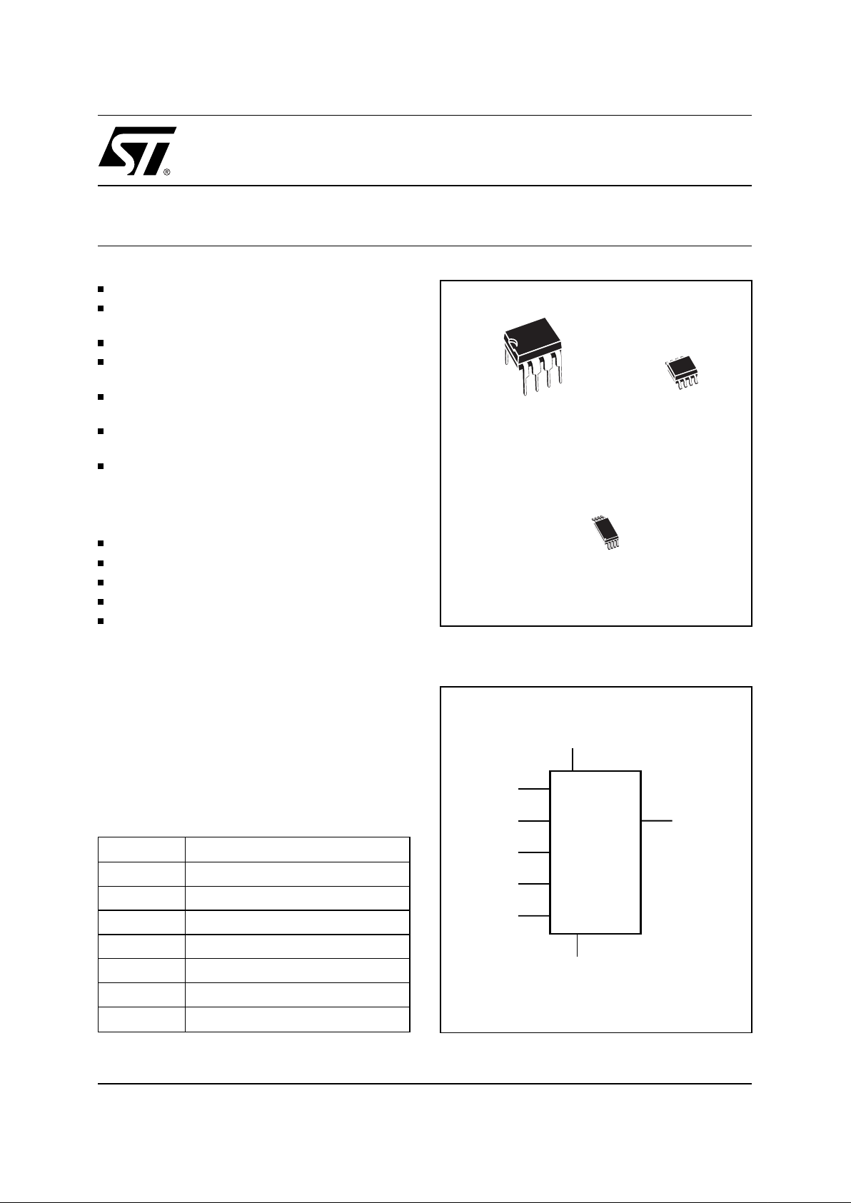
AI02020
D
V
CC
M93Sx6
V
SS
C Q
PRE
W
S
Figure 1. Logic Diagram
INDUSTRY STANDARD MICROWIRE BUS
1 MILLION ERASE/WRITE CYCLES, with
40 YEARS DATA RETENTION
SINGLE ORGANIZATION by WORD (x16)
WORD and ENTIRE MEMORY
PROGRAMMING INSTRUCTION S
SELF-TIMED PROGRAMMING CY CLE with
AUTO-ERASE
READY/BUSY SIGNAL DURING
PROGRAMMING
SINGLE SUPPLY VOLTAGE:
– 4.5V to 5.5V for M9 3Sx6 version
– 2.5V to 5.5V for M93Sx6-W version
– 1.8V to 3.6V for M93Sx6-R version
USER DEFINED WRITE PROTE CT ED AREA
PAGE WRITE MODE (4 words)
SEQUENTIAL READ OPERATION
5ms TYPICAL PROGRAMMING TIME
ENHANCED ESD and LATCH-UP
PERFORMANCES
DESCRIPTION
This M93S46/S56/S66 specification covers a
range of 4K/2K/1K bit serial EEPROM products
respectively . In this text, products are referred to as
M93Sx6. The M93Sx6 is an Electrically Erasable
Programmable Memory (EEPROM) fabricated with
STMicroelectronics’s High Endurance Single
Polysilicon CMOS technology .
S Chip Select Input
D Serial Data Input
Q Serial Data Output
C Serial Clock
PRE Protect Enable
W Write Enable
V
CC
Supply Voltage
V
SS
Ground
T ab le 1. Signal Names
8
1
SO8 (MN)
150mil Width
8
1
PSDIP8 (BN)
0.25mm Frame
8
1
TSSOP8 (DW)
169mil Width
The M93Sx6 memory is ac ces sed through a ser ial
input (D) and output (Q) using the MICROWIRE
bus protocol. The M93Sx6 is specified at 5V ±10%,
the M93Sx6-W specified at 2.5V to 5.5V and the
M93Sx6-R specified at 1.8V to 3.6V.
The M93S66/S56/S46 memory is divided into
256/128/64 x16 bit words respectively. These
memory devices are available in both PSDIP8,
SO8 and TSSOP8 packages.
The M93Sx6 memory is accessed by a set of
instructions which includes Read, Write, Page
V
SS
Q
W
PREC
SV
CC
D
AI02021
M93Sx6
1
2
3
4
8
7
6
5
Figure 2A. DIP Pin Connections
1
V
SS
Q
W
PREC
SV
CC
D
AI02022
M93Sx6
2
3
4
8
7
6
5
Figure 2B. SO and TSSOP Pin Connections
DESCRIPTION (cont’d) Write, Write All and instructions used to set the
memory protection. A Read instruction loads the
address of the first word to be read into an internal
address pointer . The data contained at this address
is then clocked out serially. The address pointer is
automatically incremented after the data is output
and, if the Chip Select input (S) is held High, the
M93Sx6 can output a sequential stream of data
words. In this way, the memory can be read as a
data stream from 16 to 4096 bits (for the M93S66),
or continuously as the address counter automatically rolls over to ’00’ when the highest address is
reached.
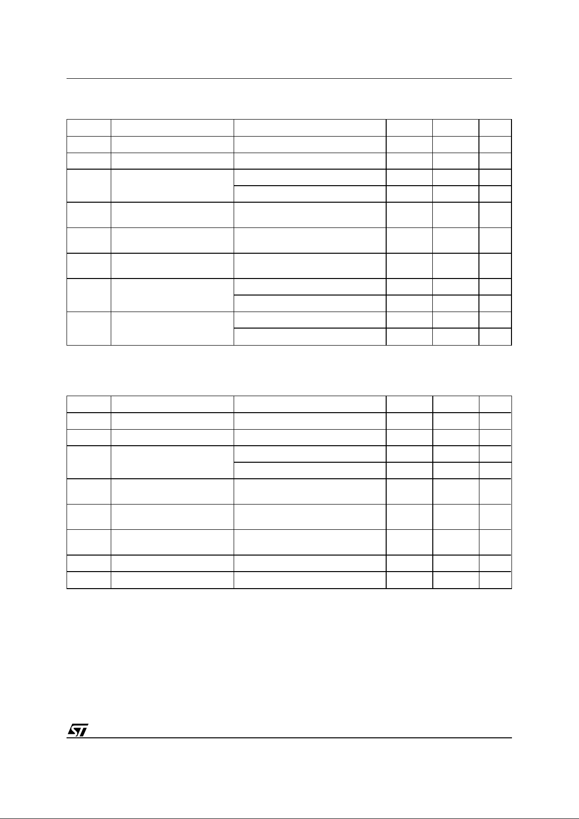
Symbol Parameter Value Unit
T
A
Ambient Operating Temperature –40 to 125
°
C
T
STG
Storage Temperature –65 to 150
°
C
T
LEAD
Lead T e mperature, Soldering (SO8 package)
(PSDIP8 package)
40 sec
10 sec
215
260
°
C
V
IO
Input or Output Voltages (Q = VOH or Hi-Z) –0.3 to VCC +0.5 V
V
CC
Supply Voltage –0.3 to 6.5 V
V
ESD
Electrostatic Discharge Voltage (Human Body model)
(2)
4000 V
Electrostatic Discharge Voltage (Machine model)
(3)
500 V
Notes:
1. Except for the rating "Operating Temperature Range", stresses above those listed in the Table "Absolute Maximum Ratings"
may cause permanent damage to the device. These are stress rating s only and operation of the device at these or any other
conditions above those indicated in the Operating sections of this specification is not implied. Exposure to Absolute Maximum
Rating conditions for extended periods may affect device reliability. Refer also to the STMicroelectronics SURE Program and other
relevant quality documents.
2. MIL-STD-883C, 3015.7 (100pF, 1500 Ω).
3. EIAJ IC-121 (Condition C) (200pF, 0 Ω).
T ab le 2. Absolute Maximum Ratings
(1)
2/23
M93S66, M93S56, M93S46
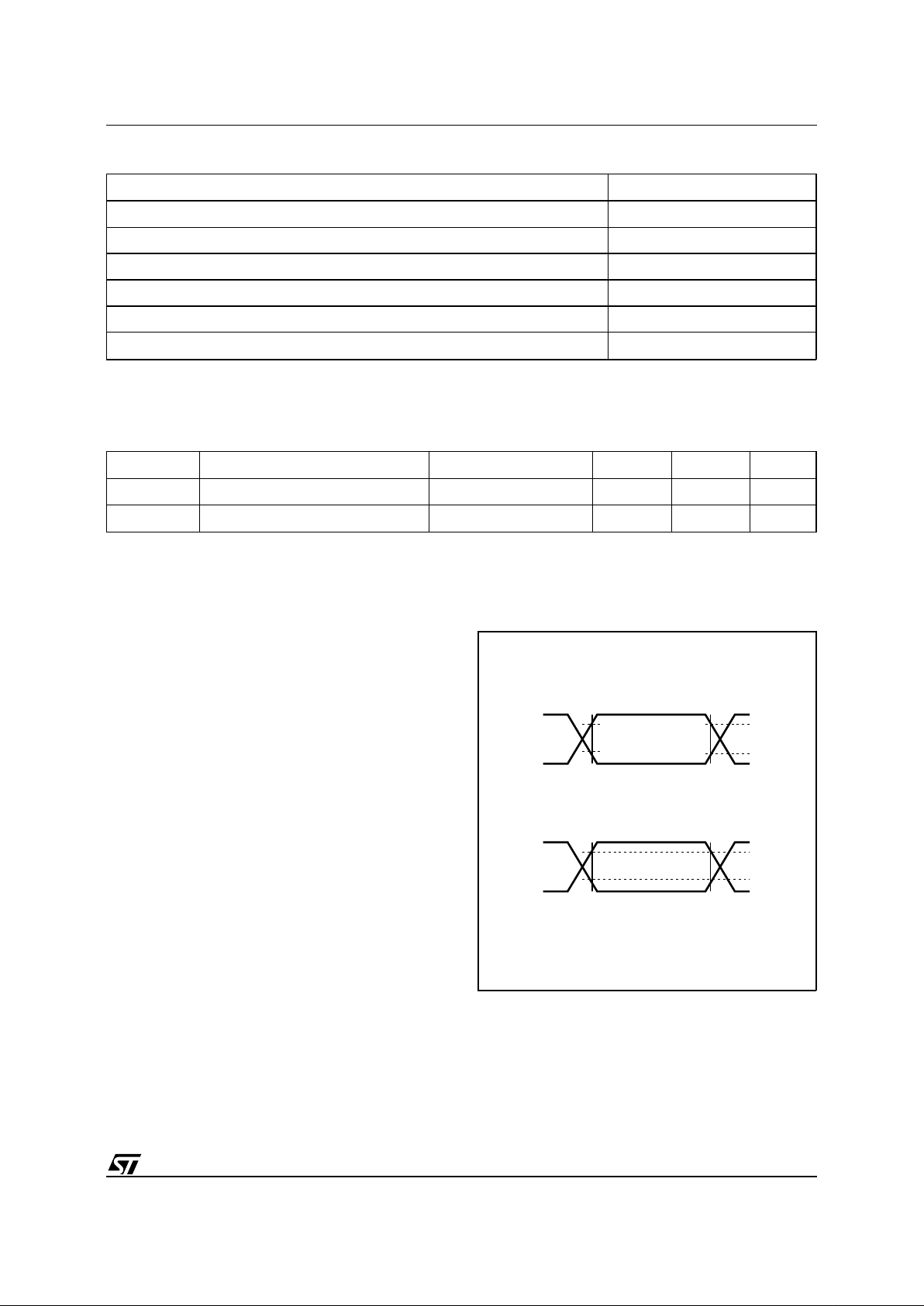
Input Rise and Fall Times
≤
50ns
Input Pulse Voltages (M93Sxx) 0.4V to 2.4V
Input Pulse Voltages (M93Sxx-W, M93Sxx-R) 0.2V
CC
to 0.8V
CC
Input Timing Reference Voltages (M93Sxx) 1.0V to 2.0V
Output Timing Reference Voltages (M93Sxx) 0.8V to 2.0V
Input and Output Timing Reference Voltages (M93Sxx-W, M93Sxx-R) 0.3V
CC
to 0.7V
CC
Output Load CL = 100pF
Note that Output Hi-Z is defined as the point where data is no longer driven.
T ab le 3. AC Measurement Conditions
AI02791
2.4V
0.4V
2.0V
0.8V
2V
1V
INPUT OUTPUT
0.8V
CC
0.2V
CC
0.7V
CC
0.3V
CC
M93SXX-W & M93SXX-R
M93SXX
Figure 3. AC Testing Input Output Waveforms
Symbol Parameter Test Condition Min Max Unit
C
IN
Input Capacitance VIN = 0V 5 pF
C
OUT
Output Capacitance V
OUT
= 0V 5 pF
Note:
1. Sampled only, not 100% tested.
T ab le 4. Capacitance
(1)
(T
A
= 25 °C, f = 1 MHz )
Within the time required by a programming cycle
(t
W
), up to 4 words may be written with help of the
Page Write instruction. the whole memory may also
be erased, or set to a predetermined pattern, by
using the Write All instruction.
Within the memory, an user defined area may be
protected against further Write instructions. The
size of this area is defined by the content of a
Protect Register, located outside of the memory
array. As a final prot ection s tep, data may be permanently protected by programming a One Time
Programming bit (OTP bit) which locks the Protect
Register content.
Programming is internally self-timed (the external
clock signal on C input may be disconnected or left
running after the start of a Write cycle) and does
not require an erase cycle prior to t he Write instruction. The Write instruction writes 16 bits at one time
into one of the 256/128/64 words of the
M93S46/S56/S66 respectively, the Page Write instruction writes up to 4 words of 16 bits to sequential locations, assuming in both cases that all
addresses are outside the Write Protected area.
After the start of the programming cycle, a
Ready/Busy signal is available on the Data output
(Q) when Chip Select (S) is driven High.
An internal feature of the M93Sx6 provides Poweron Data Protection by inhibiting any operation
when the Supply is too low. The design of the
M93Sx6 and the High Endurance CMOS technology used for its fabrication give an Erase/Write
cycle Endurance of 1,000,000 cycles and a data
retention of 40 years.
3/23
M93S66, M93S56, M93S46
Symbol Parameter Test Condition Min Max Unit
I
LI
Input Leakage Current 0V ≤ VIN ≤ V
CC
±
2.5
µ
A
I
LO
Output Leakage Current 0V ≤ V
OUT
≤ VCC, Q in Hi-Z
±
2.5
µ
A
I
CC
Supply Current VCC = 5V, S = VIH, f = 1 MHz 1.5 mA
I
CC1
Supply Current (Standby)
V
CC
= 5V, S = VSS, C = VSS,
W = V
SS
or VCC, PRE = VSS or VCC
50
µ
A
V
IL
Input Low Voltage
(D, C, S, W, PRE)
–0.3 0.8 V
V
IH
Input High Voltage
(D, C, S, W, PRE)
2V
CC
+ 1 V
V
OL
Output Low Voltage (Q) VCC = 5V, IOL = 2.1mA 0.4 V
V
OH
Output High Voltage (Q) VCC = 5V, IOH = –400µA 2.4 V
T ab le 5A. DC Characteristics for M93Sx6
(T
A
= 0 to 70°C or –40 to 85°C; VCC = 4.5V to 5.5V)
Symbol Parameter Test Condition Min Max Unit
I
LI
Input Leakage Current 0V ≤ VIN ≤ V
CC
±
2.5
µ
A
I
LO
Output Leakage Current 0V ≤ V
OUT
≤ VCC, Q in Hi-Z
±
2.5
µ
A
I
CC
Supply Current VCC = 5V, S = VIH, f = 1 MHz 1.5 mA
I
CC1
Supply Current (Standby)
V
CC
= 5V, S = VSS, C = VSS,
W = V
SS
or VCC, PRE = VSS or VCC
50
µ
A
V
IL
Input Low Voltage
(D, C, S, W, PRE)
–0.3 0.8 V
V
IH
Input High Voltage
(D, C, S, W, PRE)
2V
CC
+ 1 V
V
OL
Output Low Voltage (Q) VCC = 5V, IOL = 2.1mA 0.4 V
V
OH
Output High Voltage (Q) VCC = 5V, IOH = –400µA 2.4 V
T ab le 5B. DC Characteristics for M93Sx6
(T
A
= –40 to 125°C; VCC = 4.5V to 5.5V)
4/23
M93S66, M93S56, M93S46
Symbol Parameter Test Condition Min Max Unit
I
LI
Input Leakage Current 0V ≤ VIN ≤ V
CC
±
2.5
µ
A
I
LO
Output Leakage Current 0V ≤ V
OUT
≤ VCC, Q in Hi-Z
±
2.5
µ
A
I
CC
Supply Current (CMOS Inputs)
V
CC
= 5V, S = VIH, f = 1 MHz 1.5 mA
V
CC
= 2.5V, S = VIH, f = 1 MHz 1 mA
I
CC1
Supply Current (Standby)
V
CC
= 2.5V, S = VSS, C = VSS,
W = V
SS
or VCC, PRE = VSS or VCC
10
µ
A
V
IL
Input Low Voltage
(D, C, S, W, PRE)
–0.3 0.2 V
CC
V
V
IH
Input High Voltage
(D, C, S, W, PRE)
0.7 V
CC
VCC + 1 V
V
OL
Output Low Voltage (Q)
V
CC
= 5V, IOL = 2.1mA 0.4 V
V
CC
= 2.5V, IOL = 100µA 0.2 V
V
OH
Output High Voltage (Q)
V
CC
= 5V, IOH = –400µA 2.4 V
V
CC
= 2.5V, IOH = –100µAV
CC
– 0.2 V
T ab le 5C. DC Characteristics for M93Sx6-W
(T
A
= 0 to 70°C or –40 to 85°C; VCC = 2.5V to 5.5V)
Symbol Parameter Test Condition Min Max Unit
I
LI
Input Leakage Current 0V ≤ VIN ≤ V
CC
±
2.5
µ
A
I
LO
Output Leakage Current 0V ≤ V
OUT
≤ VCC, Q in Hi-Z
±
2.5
µ
A
I
CC
Supply Current (CMOS Inputs)
V
CC
= 3.6V, S = VIH, f = 1 MHz 1.5 mA
V
CC
= 1.8V, S = VIH, f = 1 MHz 1 mA
I
CC1
Supply Current (Standby)
V
CC
= 1.8V, S = VSS, C = VSS,
W = V
SS
or VCC, PRE = VSS or VCC
5
µ
A
V
IL
Input Low Voltage
(D, C, S, W, PRE)
–0.3 0.2 V
CC
V
V
IH
Input High Voltage
(D, C, S, W, PRE)
0.8 V
CC
VCC + 1 V
V
OL
Output Low Voltage (Q) VCC = 1.8V, IOL = 100µA 0.2 V
V
OH
Output High Voltage (Q) VCC = 1.8V, IOH = –100µAV
CC
– 0.2 V
Note:
1. This is preliminary data.
T ab le 5D. DC Characteristics for M93Sx6-R
(1)
(T
A
= 0 to 70°C or –20 to 85°C; VCC = 1.8V to3.6V)
5/23
M93S66, M93S56, M93S46
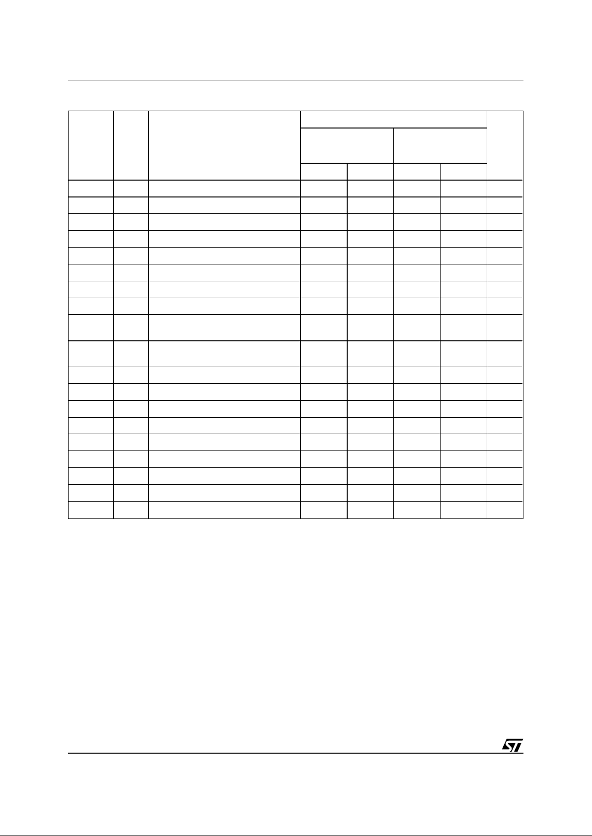
Symbol Alt Parameter
M93S66/56/46
Unit
V
CC
= 4.5V to 5.5V,
T
A
= 0 to 70°C,
T
A
= –40 to 85°C
V
CC
= 4.5V to 5.5V,
T
A
= –40 to 125°C
Min Max Min Max
t
PRVCH
t
PRES
Protect Enable Valid to Clock High 50 50 ns
t
WVCH
t
PES
Write Enable Valid to Clock High 50 50 ns
t
SHCH
t
CSS
Chip Select Set-up Time 50 50 ns
t
CLSH
t
SKS
Clock Set-up Time (relative to S) 100 100 ns
t
DVCH
t
DIS
Data In Set-up Time 100 100 ns
t
CHDX
t
DIH
Data In Hold Time 100 100 ns
t
CHQL
t
PD0
Delay to Output Low 400 400 ns
t
CHQV
t
PD1
Delay to Output Valid 400 400 ns
t
CLPRX
t
PREH
Clock Low to Protect Enable
Transition
00ns
t
SLWX
t
PEH
Chip Select Low to Write Enable
Transition
250 250 ns
t
CLSL
t
CSH
Chip Select Hold Time 0 0 ns
t
SLCH
Chip Select Low to Clock High 250 250 ns
t
SLSH
(1)
t
CS
Chip Select Low to Chip Select High 250 250 ns
t
SHQV
t
SV
Chip Select to Ready/Busy Status 400 400 ns
t
SLQZ
t
DF
Chip Select Low to Output Hi-Z 200 200 ns
t
CHCL
(2)
t
SKH
Clock High Time 250 250 ns
t
CLCH
(2)
t
SKL
Clock Low Time 250 250 ns
t
W
t
WP
Erase/Write Cycle time 10 10 ms
f
C
f
SK
Clock Frequency 0 1 0 1 MHz
Notes:
1. Chip Select must be brought low for a minimum of tSLSH between consecutive instructions cycles.
2. The Clock frequency specification calls for a minimum clock period of 1/fC, therefore the sum of the timings tCHCL+tCLCH
must be greater or equal to 1/fC.
T ab le 6A. AC Characteristics
6/23
M93S66, M93S56, M93S46
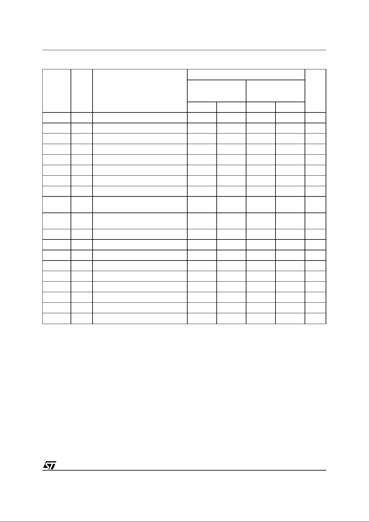
Symbol Alt Parameter
M93S66/56/46
Unit
V
CC
= 2.5V to 5.5V,
T
A
= 0 to 70°C,
T
A
= –40 to 85°C
V
CC
= 1.8V to 3.6V,
(3)
TA = 0 to 70°C
T
A
= –20 to 85°C
Min Max Min Max
t
PRVCH
t
PRES
Protect Enable Valid to Clock High 50 50 ns
t
WVCH
t
PES
Write Enable Valid to Clock High 50 50 ns
t
SHCH
t
CSS
Chip Select Set-up Time 100 200 ns
t
CLSH
t
SKS
Clock Set-up Time (relative to S) 100 100 ns
t
DVCH
t
DIS
Data In Set-up Time 100 100 ns
t
CHDX
t
DIH
Data In Hold Time 100 200 ns
t
CHQL
t
PD0
Delay to Output Low 400 700 ns
t
CHQV
t
PD1
Delay to Output Valid 400 700 ns
t
CLPRX
t
PREH
Clock Low to Protect Enable
Transition
00ns
t
SLWX
t
PEH
Chip Select Low to Write Enable
Transition
250 250 ns
t
CLSL
t
CSH
Chip Select Hold Time 0 0 ns
t
SLCH
Chip Select Low to Clock High 250 250 ns
t
SLSH
(1)
t
CS
Chip Select Low to Chip Select High 250 1000 ns
t
SHQV
t
SV
Chip Select to Ready/Busy Status 400 700 ns
t
SLQZ
t
DF
Chip Select Low to Output Hi-Z 200 200 ns
t
CHCL
(2)
t
SKH
Clock High Time 350 800 ns
t
CLCH
(2)
t
SKL
Clock Low Time 250 800 ns
t
W
t
WP
Erase/Write Cycle time 10 10 ms
f
C
f
SK
Clock Frequency 0 1 0 0.5 MHz
Notes:
1. Chip Select must be brought low for a minimum of tSLSH between consecutive instructions cycles.
2. The Clock frequency specification calls for a minimum clock period of 1/fC, therefore the sum of the timings tCHCL+tCLCH
must be greater or equal to 1/fC.
3. This is preliminary data.
T ab le 6B. AC Characteristics
7/23
M93S66, M93S56, M93S46
 Loading...