

SGS Thomson Microelectronics M93C86-R, M93C06-R, M93C56-R, M93C46-R, M93C66-R Datasheet
...
1/27May 2003
M93C86, M93C76, M93C66
M93C56, M93C46, M93C06
16K bit, 8Kbit, 4Kbit , 2Kbi t, 1Kbit and 256bit (8-bit or 16-bit wide)
MICROWIRE Serial Access EEPROM
FEATURES SUMMARY
■ Industry Standard MICROWIRE Bus
■ Single Supply Voltage:
– 4.5V to 5.5V for M93Cx6
– 2.5V to 5.5V for M93Cx6-W
– 1.8V to 5.5V for M93Cx6-R
■ Dual Organization: by Word (x16) or Byte (x8)
■ Programming Instructions that work on: Byte,
Word or Entire Memory
■ Self-timed Programming Cycle with Auto-Erase
■ Ready/Busy Signal During Programming
■ Speed:
– 1MHz Clock Rate, 10ms Write Time (Current
product, identified by process identification
letter F or M)
– 2MHz Clock Rate, 5ms Write Time (New
Product, identified by process identification
letter W)
■ Sequential Read Operation
■ Enhanced ESD/Latch-Up B ehaviour
■ More than 1 Million Erase/Write Cycles
■ More than 40 Year Data Retention
Figure 1. Packages
M93C06 IS “NOT FOR NEW DESIGN”
The M93C06 is still in production, but is not recommended for new de signs. Please ref er to AN1571
on how to replace the M93C06 by the M93C46 in
your application.
PDIP8 (BN)
8
1
SO8 (MN)
150 mil width
8
1
TSSOP8 (DW)
169 mil width
TSSOP8 (DS)
3x3mm body size

M93C86, M93C76, M93C66, M93C56, M93C46, M93C06
2/27
SUMMARY DESCRIPTION
These electrically erasable programm able memory (EEPROM) devices are accessed through a Serial Data Input (D) and Serial Data Output (Q)
using the MICROWIRE bus protocol.
Figure 2. Logic Diagram
Table 1. Signal Names
The memory array organization may be divided
into either bytes (x8) or words (x16) which may be
selected by a signal applie d on O rganization Select (ORG). The bit, byte and word sizes of the
memories are as shown in Table 2.
Table 2. M em ory Size versus Organi za tion
Note: 1. Not for Ne w Design
The M93Cx6 is acces sed by a set of instructions,
as summarized in Table 3, and in more detail in
Table 4 to Table 6).
Table 3. Instruction Set for the M93Cx6
A Read Data from Memory (READ) instruction
loads the address of t he first byte or word to be
read in an internal addres s register. The data at
this address is then clocked out serially. The address register is automatically incremented after
the data is output and, if Chip Select Input (S) is
held High, the M93Cx6 can output a sequential
stream of data bytes or words. In this way, the
memory can be read as a d ata stream from eight
to 16384 bits long (in the case of the M93C86), or
continuously (the address counter automatically
rolls over to 00h when the highest address is
reached).
Programming is internally sel f-timed (the external
clock signal on Serial Clock (C) may be stopped or
left running after the start of a Write cycle) and
does not require an Erase cycle prior to the Write
instruction. The Write instruction writes 8 or 16 bits
at a time into one of the b yte or word locat ions of
the M93Cx6. After the start of the programming cy-
S Chip Select Input
D Serial Data Input
Q Serial Data Output
C Ser ial Clock
ORG Organisation Select
V
CC
Supply Voltage
V
SS
Ground
AI01928
D
V
CC
M93Cx6
V
SS
C
Q
S
ORG
Device
Number
of Bits
Number
of 8-bit
Bytes
Number
of 16-bit
Words
M93C86 16384 2048 1024
M93C76 8192 1024 512
M93C66 4096 512 256
M93C56 2048 256 128
M93C46 1024 128 64
M93C06
1
256 32 16
Instruction Description Data
READ Read Data from Memory Byte or Word
WRITE Write Data to Memory Byte or Word
EWEN Erase/Write Enable
EWDS Erase/Write Disable
ERASE Erase Byte or Word Byte or Word
ERAL Erase All Memory
WRAL
Write All Memory
with same Data
3/27
M93C86, M93C76, M93C66, M 93C56, M93C46, M93C06
cle, a Busy/Ready signal is available on Serial
Data Output (Q) when Chip Select Input (S) is driven High.
An internal Power-on Dat a P rotec tion m echani sm
in the M93Cx6 inhibits the device when the supply
is too low.
Figure 3. DIP, SO and TSSOP Connections
Note: 1. See page 21 (onwards) for package dimensions, and how
to identify pin-1.
2. DU = Don’t Use.
Figure 4. 90° Turned-SO Connections
Note: 1. See page 24 for package dimensions, and how to identify
pin-1.
2. DU = Don’t Use.
The DU (Don’t Use) pin does not contribute to the
normal operation of the device. It is reserved for
use by STMicroelectronics during test sequences.
The pin may be left unconnec ted or may be connected to V
CC
or VSS. Direct connection of DU to
V
SS
is recommended for the lowest stand-by pow-
er consumption.
MEMORY ORGANIZATION
The M93Cx6 memory is organized either as bytes
(x8) or as words (x16). If Organization Select
(ORG) is le ft unconnected (or con nected to V
CC
)
the x16 organization is selected; when Organization Select (ORG) is c onnected to Ground (V
SS
)
the x8 organization is selected. When the M93Cx6
is in stand-by mode, Organization Select (ORG)
should be set either to V
SS
or VCC for minimum
power consumption. Any voltage between V
SS
and VCC applied to Organization Select (ORG)
may increase the stand-by current.
POWER-ON DA TA PROTECTI ON
To prevent data corruption and inadvertent write
operations during power-up, a Power-On Reset
(POR) circuit resets all internal programming circuitry, and sets the device in the Write Disable
mode.
– At Power-up and P ower-dow n, the d evic e m ust
not
be selected (that is, Chip Select Input (S)
must be driven Low) until the supply voltage
reaches the operating value V
CC
specified in
Table 8 to Table 10.
– When V
CC
reaches its valid level, the d evice is
properly reset (in the Write Disable mode) and
is ready to decode and execute incoming instructions.
For the M93Cx6 devices (5V range) the POR
threshold voltage is around 3V. For the M 93Cx6W (3V range) and M93Cx6-R (2V range) the POR
threshold voltage is around 1.5V.
V
SS
Q
ORG
DUC
SV
CC
D
AI01929B
M93Cx6
1
2
3
4
8
7
6
5
1
V
SS
Q
ORGDU
C
S
V
CC
D
AI00900B
M93Cx6
2
3
4
8
7
6
5
M93C86, M93C76, M93C66, M93C56, M93C46, M93C06
4/27
INSTRUCTIONS
The instruction set of the M93Cx6 devices contains seven instructions, as summarized in Table 4
to Table 6. Each instruction consists of the following parts, as shown in Figure 5:
■ Each instruction is preceded by a rising edge on
Chip Select Input (S) with Serial Clock (C) being
held Low.
■ A start bit, which is the first ‘1’ read on Serial
Data Input (D) during the rising edge of Serial
Clo c k (C ).
■ Two op-code bits, read on Serial Data Input (D)
during the rising edge of Serial Clock (C).
(Some instructions also use the first two bits of
the address to define the op-code).
■ The address bits of the byte or word that is to be
accessed. For the M93C46, the address is
made up of 6 bits for the x16 organization or 7
bits for the x8 organization (see Table 4). For
the M93C56 and M93C66, the address is made
up of 8 bits for the x16 organization or 9 bits for
the x8 organization (see Table 5). For the
M93C76 and M93C86, the address is made up
of 10 bits for the x16 organization or 11 bits for
the x8 organization (see Table 6).
The M93Cx6 devices are fabricated in CMOS
technology and are therefore able to run as slow
as 0 Hz (static input signals) or as fast as the maximum ratings specified in Table 19 to Table 22.
Table 4. Instruction Set for the M93C46 and M93C06
Note: 1. X = Don’t Care bit.
2. Address bits A6 and A5 are not decoded by the M93C06 .
3. Address bits A5 and A4 are not decoded by the M93C06 .
Instruc
tion
Description
Start
bit
Op-
Code
x8 Origination (ORG = 0) x16 Origination (ORG = 1)
Address
1,2
Data
Required
Clock
Cycles
Address
1,3
Data
Required
Clock
Cycles
READ
Read Data from
Memory
1 10 A6-A0 Q7-Q0 A5-A0 Q15-Q0
WRITE
Write Data to
Memory
1 01 A6-A0 D7-D0 18 A5-A0 D15-D0 25
EWEN Erase/Write Enable 1 00 11X XXXX 10 11 XXXX 9
EWDS Erase/Write Disable 1 00 00X XXXX 10 00 XXXX 9
ERASE Erase Byte or Word 1 11 A6-A0 10 A5-A0 9
ERAL Erase All Memory 1 00 10X XXXX 10 10 XXXX 9
WRAL
Write All Memory
with same Data
1 0 0 01X XXXX D7-D0 18 01 XXXX D15-D0 25
5/27
M93C86, M93C76, M93C66, M 93C56, M93C46, M93C06
Table 5. Instruction Set for the M93C56 and M93C66
Note: 1. X = Don’t Care bit.
2. Address bit A8 is not decoded b y t he M 93C56.
3. Address bit A7 is not decoded b y t he M 93C56.
Table 6. Instruction Set for the M93C76 and M93C86
Note: 1. X = Don’t Care bit.
2. Address bit A10 i s not decoded by the M93C76.
3. Address bit A9 is not decoded b y t he M 93C76.
Instruc
tion
Description
Start
bit
Op-
Code
x8 Origination (ORG = 0) x16 Origination (ORG = 1)
Address
1,2
Data
Required
Clock
Cycles
Address
1,3
Data
Required
Clock
Cycles
READ
Read Data from
Memory
1 10 A8-A0 Q7-Q0 A7-A0 Q15-Q0
WRITE
Write Data to
Memory
1 01 A8-A0 D7-D0 20 A7-A0 D15-D0 27
EWEN Erase/Write Enable 1 00
1 1XXX
XXXX
12
11XX
XXXX
11
EWDS Erase/Write Disable 1 00
0 0XXX
XXXX
12
00XX
XXXX
11
ERASE Erase Byte or Word 1 11 A8-A0 12 A7-A0 11
ERAL Erase All Memory 1 00
1 0XXX
XXXX
12
10XX
XXXX
11
WRAL
Write All Memory
with same Data
100
0 1XXX
XXXX
D7-D0 20
01XX
XXXX
D15-D0 27
Instruc
tion
Description
Start
bit
Op-
Code
x8 Origination (ORG = 0) x16 Origination (ORG = 1)
Address
1,2
Data
Required
Clock
Cycles
Address
1,3
Data
Required
Clock
Cycles
READ
Read Data from
Memory
1 10 A10-A0 Q7-Q0 A9-A0 Q15-Q0
WRITE
Write Data to
Memory
1 01 A10-A0 D7-D0 22 A9-A0 D15-D0 29
EWEN Erase/Write Enable 1 00
11X XXXX
XXXX
14
11 XXXX
XXXX
13
EWDS Erase/Write Disable 1 00
00X XXXX
XXXX
14
00 XXXX
XXXX
13
ERASE Erase Byte or Word 1 11 A10-A0 14 A9-A0 13
ERAL Erase All Memory 1 00
10X XXXX
XXXX
14
10 XXXX
XXXX
13
WRAL
Write All Memory
with same Data
100
01X XXXX
XXXX
D7-D0 22
01 XXXX
XXXX
D15-D0 29

M93C86, M93C76, M93C66, M93C56, M93C46, M93C06
6/27
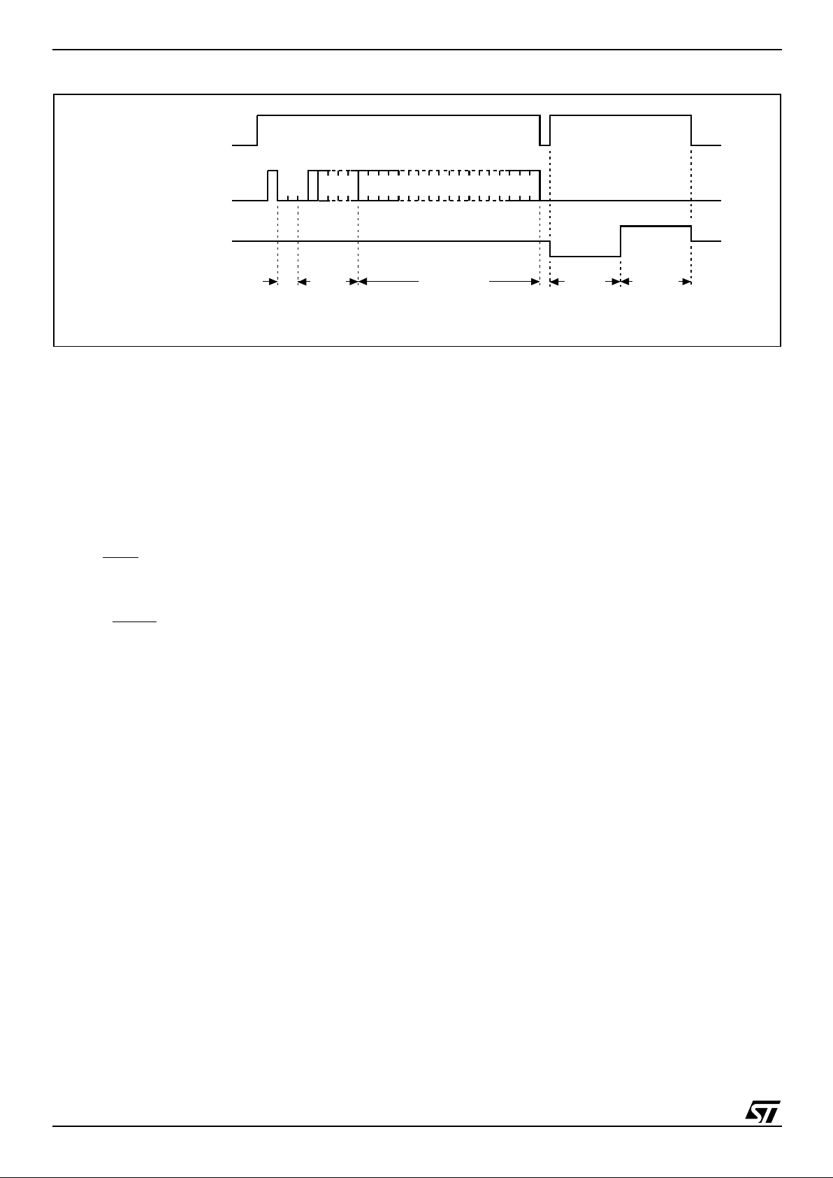
Figure 5. READ, WRITE, EWEN, EWDS Sequences
Note: For the mea ni ngs of An, Xn, Qn and Dn, see Table 4, Table 5 and Table 6.
Read
The Read Data from Memory (READ) instruction
outputs serial data on Serial Data Output (Q).
When the instruction is received, the op-code and
address are decoded, and the data from the memory is transferred to an output shift register. A dummy 0 bit is output first, followed by the 8-bit byte or
the 16-bit word, with the m ost significant bit first.
Output data changes are triggered by the rising
edge of Serial Clock (C). The M93Cx6 automatically increments the internal address register and
clocks out the next byte (or word) as long as the
Chip Se lect Input (S) is hel d High. In this ca se, the
dummy 0 bit is
not
output between bytes (or
words) and a continuous stream of data can be
read.
Erase/Write Enable and Disable
The Erase/Write Enable (EWEN) instruction enables the future execution of erase or write instructions, and the Erase/Write Disable (EWDS)
instruction disables it. When power is first applied,
the M93Cx6 initializes itself so that erase and write
instructions are disabled. After an Erase/Write Enable (EWEN) instruction has been executed, erasing and writing remains enabled until an Erase/
Write Disable (EWDS) instruction is executed , or
until V
CC
falls below the power-on reset threshold
voltage. To protect the memory contents from accidental corruption, it is advisable to issue the
Erase/Write Disable (EWDS) instruction a fter every write cycle. The Read Data from Memory
(READ) instruction is not affected by the Erase/
Write Enable (EWEN) or Erase/Write Disable
(EWDS) instructions.
AI00878C
1 1 0 An A0
Qn Q0
DATA OUT
D
S
Q
READ
SWRITE
ADDR
OP
CODE
1 0An A0
DATA IN
D
Q
OP
CODE
Dn D01
BUSY READY
SERASE
WRITE
ENABLE
1
0XnX0
D
OP
CODE
101
SERASE
WRITE
DISABLE
1 0XnX0D
OP
CODE
0 00
CHECK
STATUS
ADDR

7/27
M93C86, M93C76, M93C66, M 93C56, M93C46, M93C06
Figure 6. ERASE, ERAL Sequences
Note: For the mea ni ngs of An and Xn, please see Table 4, Ta bl e 5 and Table 6.
Erase
The Erase Byte or Word (ERASE) instruction sets
the bits of the addressed memory byte (or word) to
1. Once the addres s has been correc tly dec oded,
the falling edge of the Chip Select Input (S) starts
the self-timed Erase cycle. The compl etion of the
cycle can be detected by monitoring the Ready/
Busy
line, as described on page 7.
Write
For the Write Data to Memory (WRITE) instruction,
8 or 16 data bits follow the op-code and address
bits. These form the byte or word that is to be written. As with the other bits, Serial Data Input (D) is
sampled on the rising edge of Serial Clock (C).
After the last data bit has been samp led,
the Chip
Select Input (S) must be taken Low before the next
rising edge of Serial Clock (C).
If Chip Select Input
(S) is brought Low before or after this specific time
frame, the self-timed programming cycle will not
be started, and the addressed location will not be
programmed. The completion of the cycle can be
detected by monitoring the Ready/Busy
line, as
described later in this document.
Once the Write cycle has been started, it is inter-
nally self-timed (the external clock signal on Serial
Clock (C) may be stopped or left running after the
start of a Write cycle). The cycle is automatically
preceded by an Erase c ycle, so it is unne cessary
to execute an explicit erase instruction before a
Write Data to Memory (WRITE) instruction.
Erase All
The Eras e All Memory (ER AL) instruction erases
the whole memory (all mem ory bits are set to 1).
The format of the instru ction requires that a dum my address be provided. The E rase cycle is conducted in the sam e way as the Erase instruction
(ERASE). The completion of the cycle can be detected by monitoring the Ready/Busy
line, as de-
scribed on page 7.
AI00879B
SERASE
1 1D
Q
ADDR
OP
CODE
1
BUSY READY
CHECK
STATUS
SERASE
ALL
1 0D
Q
OP
CODE
1
BUSY READY
CHECK
STATUS
0 0
An A0
Xn X0
ADDR
M93C86, M93C76, M93C66, M93C56, M93C46, M93C06
8/27
Figure 7. WRAL Sequence
Note: For the mea ni ngs of Xn and Dn, please see Table 4, Table 5 and Tabl e 6.
Write All
As with the Erase All Memory (ERAL) instruction,
the format of the Write All Memory with same Data
(WRAL) instruction requires that a dummy address be provided. As with the Write Data to Memory (WRITE) instruction, the format of the Write All
Memory with same Data (WRAL) instruction requires that an 8-bit data by te , or 16-bit data word,
be provided. This value is written to all the addresses of the mem ory device. T he completion of
the cycle can be detected by monitoring the
Ready/Busy
line, as described next.
READY/BUSY
STATUS
While the Write or Erase cycle is underway, for a
WRITE, ERASE, WRAL or ERAL instruction, the
Busy signal (Q=0) is returned whenever Chip Select Input (S) is driven High. (Please note, though,
that there is an initial delay, of t
SLSH
, before this
status information becomes available). In this
state, the M93 Cx6 ignores any data on the bus.
When the Write cycle is completed, and Chip Select Input (S) is driven High, the Ready signal
(Q=1) indicates that the M93Cx6 is ready to receive the next instruction. Serial Data Output (Q)
remains set to 1 until the Chip Select Input (S) is
brought Low or until a new start bit is decoded.
COMMON I/O OPERATION
Serial Data Output (Q) a nd Serial Data Input (D)
can be conne cted toget her, th rough a current limiting resistor, to form a common, single-wire data
bus. Some precautions must be taken when operating the memory in this way, mostly to prevent a
short circuit current from flowing when the last address bit (A0) clashes with the first data bit on Serial Data Output (Q). Please see the application
note
AN394
for details.
AI00880C
SWRITE
ALL
DATA IN
D
Q
ADDR
OP
CODE
Dn D0
BUSY READY
CHECK
STATUS
1
0 00 1 Xn X0
9/27
M93C86, M93C76, M93C66, M 93C56, M93C46, M93C06
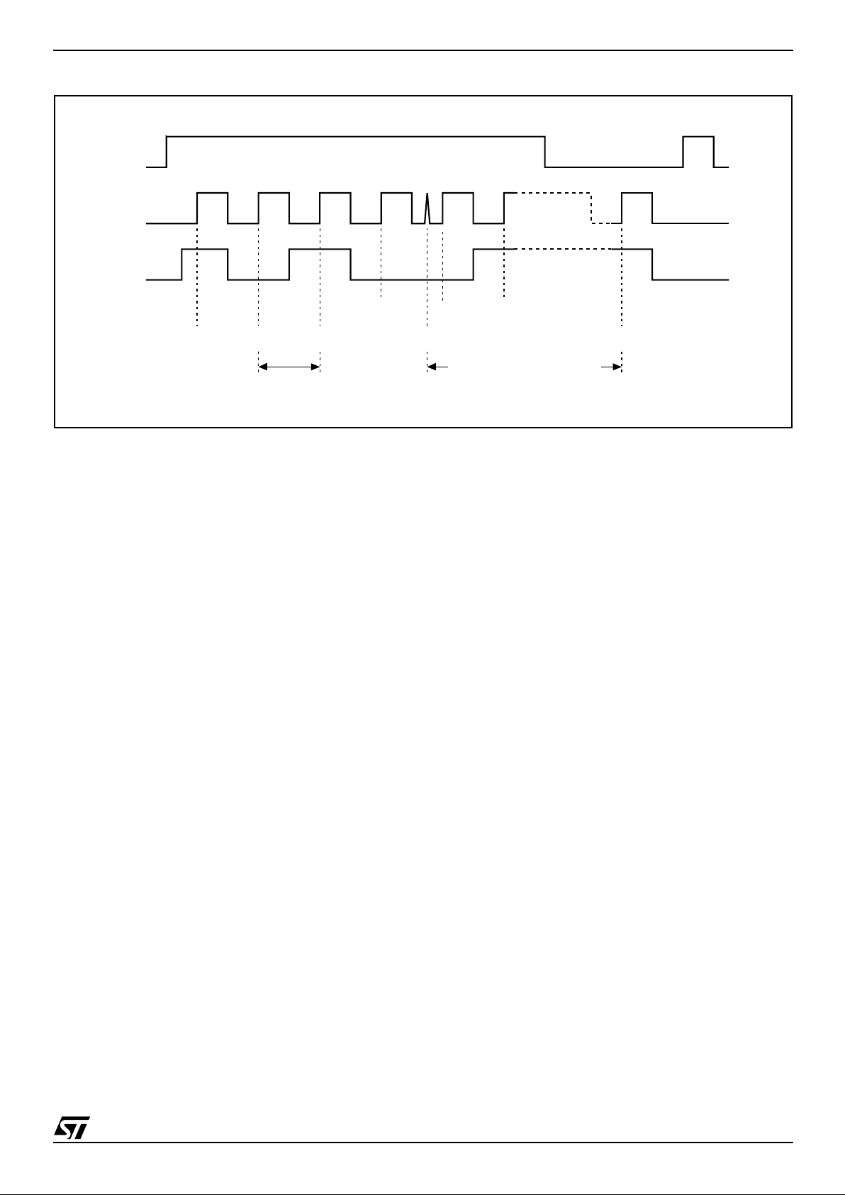
Figure 8. Write Sequence with One Clock Glitch
CLOCK PULSE COUNTER
In a noisy environm ent, the number o f pulses received on Serial Clock (C) may be greater than the
number delivered by the master (the microcontroller). This can lead to a misalignment of the instruction of one or more bits (as shown in Figure 8) and
may lead to the writing of erroneous data at an erroneous address.
To combat this problem, the M93Cx6 has an onchip counter that counts the clock pulses from the
start bit until the falling edge of the Chip Select Input (S). If the number of clock pulses received is
not the number expected, the WRITE, ERASE,
ERAL or WRAL instruction is aborted, and the
contents of the memory are not modified.
The number of clock cycles expe cted for each instruction, and for each member of the M93Cx6
family, are summa rized i n Table 4 to Table 6. For
example, a Write Data to Memory (WRITE) instruction on the M93C 56 (or M 93C66) ex pect s 20
clock cycles (for the x8 organizat ion) from the start
bit to the falling edge of Chip Select Input (S). That
is:
1 Start bit
+ 2 Op-code bits
+ 9 Address bits
+ 8 Data bits
AI01395
S
An-1
C
D
WRITE
START
D0"1""0"
An
Glitch
An-2
ADDRESS AND DATA
ARE SHIFTED BY ONE BIT
 Loading...