


SGS Thomson Microelectronics M93C86-W, M93C86-MN3, M93C86-BN6, M93C86-BN3, M93C86 Datasheet
...
M93C86, M93C76, M93C66
M93C56, M93C46, M93C06
16K/8K/4K/2K/1K/256 (x8/x16) Serial Microwire Bus EEPROM
February 1999 1/19
AI01928
D
V
CC
M93Cx6
V
SS
C
Q
S
ORG
Figure 1. Logic Diagram
INDUSTRY STANDARD MICROWIRE BUS
1 MILLION ERASE/WRITE CYCLES, with
40 YEARS DAT A RE TENTION
DUAL ORGANIZATION: by WORD (x16) or by
BYTE (x8 )
BYTE/WORD and ENTIRE MEMORY
PROGRAMMING INSTRUCTION S
SELF-TIMED PROGRAMMING CY CLE with
AUTO-ERASE
READY/BUSY SIGNAL DURING
PROGRAMMING
SINGLE SUPPLY VOLTAGE:
– 4.5V to 5.5V for M93Cx6 version
– 2.5V to 5.5V for M93Cx6-W version
– 1.8V to 3.6V for M93Cx6-R version
SEQUENTIAL READ OPERATION
5ms TYPICAL PROGRAMMING TIME
ENHANCED ESD/LA T CH-UP
PERFORMANCES
DESCRIPTION
This M93C86/C76/C66/C56/C46/C06 specification covers a range of 16K/8K/4K/2K/1K/256 bit
serial EEPROM products respectively. In this text,
products are referred to as M93Cx6. The M93Cx6
is an Electrically Erasable Programmable Memory
(EEPROM) fabricated with STMicroelectronics’s
High Endurance Single Polysilicon CMOS technology. The M93Cx6 memory is accessed through a
serial input (D) and output (Q) using the MICROWIRE bus protocol.
S Chip Select Input
D Serial Data Input
Q Serial Data Output
C Serial Clock
ORG Organisation Select
V
CC
Supply Voltage
V
SS
Ground
T ab le 1. Signal Names
8
1
SO8 (MN)
150mil Width
8
1
PSDIP8 (BN)
0.25mm Frame
8
1
TSSOP8 (DW)
169mil Width
The M93Cx6 specified at 5V±10%, the M93Cx6-W
specified at 2.5V to 5.5V and the M93Cx6-R specified at 1.8V to 3.6V.
The M93Cx6 memory array organization may be
divided into either bytes (x8) or words (x16) which
may be selected by a signal applied on the ORG
input. The M93C86/C76/C66/C56/C46/C06 is divided into either 2048/1024/512/256/128/32 x8 bit
bytes or 1024/512/256/128/64/16 x16 bit words
respectively. These memory devices are available
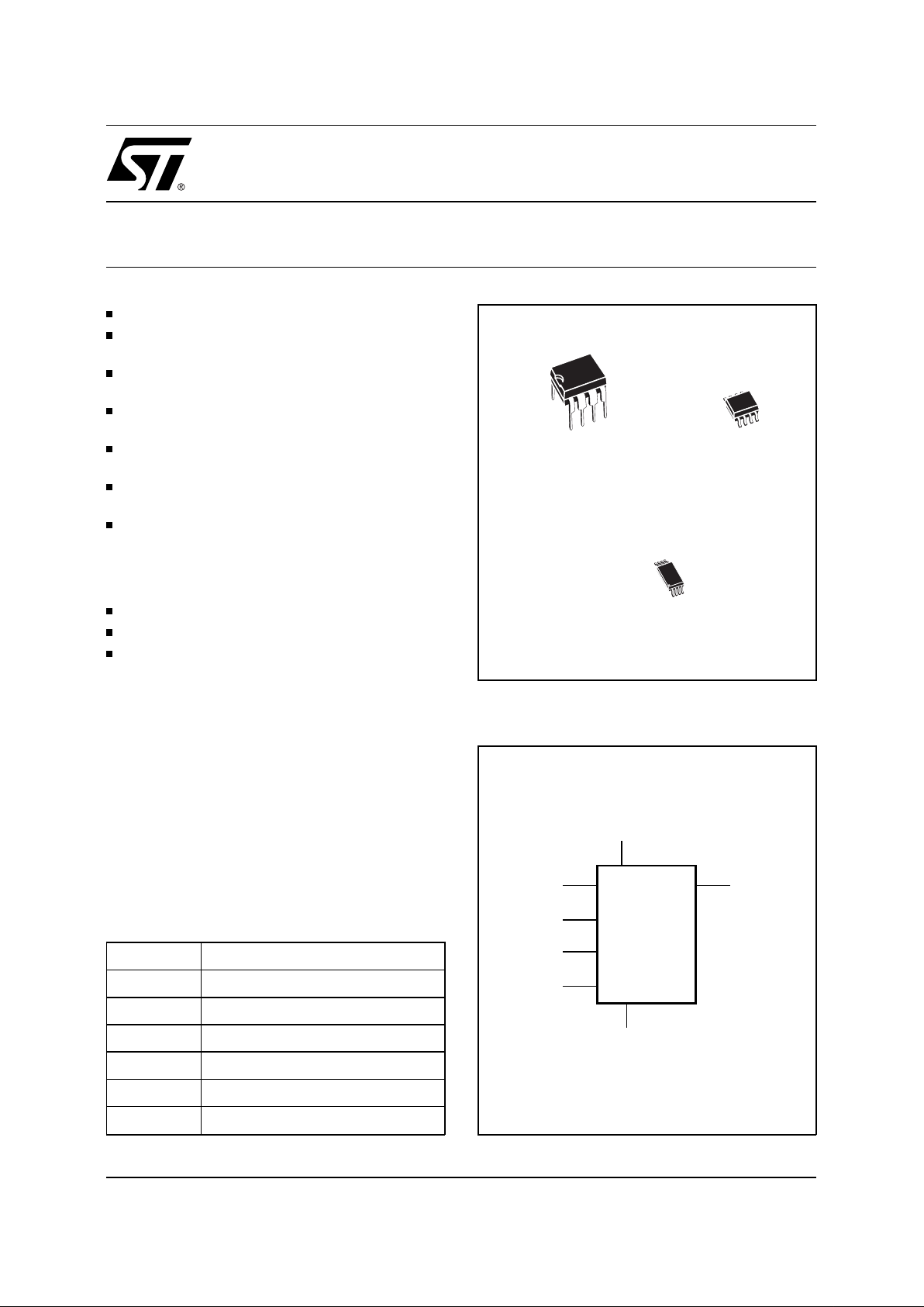
in both PSDIP8, SO8 and TSSOP8 packages.
The M93Cx6 memory is accessed by a set of
instructions which includes Read a Byte/Word,
Write a Byte/Word, Erase a Byte/Word, Erase All
and Write All. A Read instruction loads the address
of the first byte/word to be read into an internal
address pointer . The data contained at this address
is then clocked out serially. The address pointer is
automatically incremented after the data is output
and, if the Chip Select input (S) is held High, the
M93Cx6 can output a sequential stream of data
bytes/words. In this way, the memory can be read
V
SS
Q
ORG
DUC
SV
CC
D
AI01929B
M93Cx6
1
2
3
4
8
7
6
5
Figure 2A. DIP and SO Pin Connections
1
V
SS
Q
ORGDU
C
S
V
CC
D
AI00900
M93Cx6
2
3
4
8
7
6
5
Figure 2B. SO 90° Turn Pin Connections
DESCRIPTION (cont’d)
Warning:
DU = Don’t Use
as a data stream from 8 up to 16,384 bits long (for
the M93C86 only), or continuously as the address
counter automatically rolls over to ’00’ when the
highest address is reached.
Programming is internally self-timed (the external
clock signal on C input may be disconnected or left
running after the start of a Write cycle) and does
not require an erase cycle prior to t he Write instruction. The Write instruction writes 8 or 16 bits at one
time into one of the byte or word locations of the
M93Cx6. After the start of the programming cycle,
a Busy/Ready signal is available on the Data output
(Q) when Chip Select (S) is driven High.
An internal feature of the M93Cx6 provides Poweron Data Protection by inhibiting any operation
when the Supply is too low for reliable opera tion.
The design of the M93Cx6 and the H igh Endurance
CMOS technology used for its fabrication give an
Erase/Write cycle Endurance of 1,000,000 cycles
and a data retention of 40 years.
The DU (Don’t Use) pin does not af fect the function
of the memory. It is reserved for use by STMicroelectronics during test sequences. The pin may
be left unconnected or may be connected to V
CC
or VSS. Direct connection of DU to VSS is recommended for the lowest standby power consumption.
MEMORY ORGANIZATION
The M93Cx6 is organised in either bytes (x8) or
words (x16). If the ORG input is left unconnected
(or connected to V
CC
) the x16 organization is se-
lected; when ORG is connected to Ground (V
SS
)
the x8 organization is selected. When the M93Cx6
is in standby mode, the ORG input should be set
to either V
SS
or VCC in order to achiev e minimum
power consumption. Any voltage between V
SS
and
V
CC
applied to the OR G input pin may incr ease the
standby current value.
1
AI02789
2
3
4
8
7
6
5
ORG
DUC
SV
CC
D
M93C06/46/56/66 - W
M93C06/46/56/66 - R
Q
V
SS
Figure 2C. TSSOP Pin Connections
Warning:
DU = Don’t Use
Warning:
DU = Don’t Use
2/19
M93C86, M93C76, M93C66, M93C56, M93C46, M93C06
AI02553
2.4V
0.4V
2.0V
0.8V
2V
1V
INPUT OUTPUT
0.8V
CC
0.2V
CC
0.7V
CC
0.3V
CC
M93CXX-W & M93CXX-R
M93CXX
Figure 3. AC Testing Input Output Waveforms
Input Rise and Fall Times
≤
50ns
Input Pulse Voltages (M93Cxx) 0.4V to 2.4V
Input Pulse Voltages (M93Cxx-W, M93Cxx-R) 0.2V
CC
to 0.8V
CC
Input Timing Reference Voltages (M93Cxx) 1.0V to 2.0V
Output Timing Reference Voltages (M93Cxx) 0.8V to 2.0V
Input and Output Timing Reference Voltages (M93Cxx-W, M93Cxx-R) 0.3V
CC
to 0.7V
CC
Output Load CL = 100pF
Note that Output Hi-Z is defined as the point where data is no longer driven.
T ab le 3. AC Measurement Conditions
POWER-ON DATA PROTECTION
In order to prevent data corruption and inadvertent
write operations during power-up, a Power On
Reset (POR) circuit resets all internal programming
circuitry and sets the device in the Write Disable
mode.
– At Power-up and Power-down, the device must
NOT be selected (that is, the S input must be
driven low) until the supply voltage reaches the
operating value V
CC
specified in the AC and DC
tables.
– When V
CC
reaches its functional value, the device is properly reset (in the W rite Disable mode)
and is ready to decode and execute an incom ing
instruction.
For the M93Cx6 specified at 5V , the POR threshold
voltage is around 3V. For all the other M93Cx6
specified at low V
CC
(with -W and -R VCC rang e
options), the POR threshold voltage is around 1.5V.
Symbol Parameter Value Unit
T
A
Ambient Operating Temperature –40 to 125
°
C
T
STG
Storage Temperature –65 to 150
°
C
T
LEAD
Lead Temperature, Soldering (SO8 package)
(PSDIP8 package)
40 sec
10 sec
215
260
°
C
V
IO
Input or Output Voltages (Q = VOH or Hi-Z) –0.3 to VCC +0.5 V
V
CC
Supply Voltage –0.3 to 6.5 V
V
ESD
Electrostatic Discharge Voltage (Human Body model)
(2)
4000 V
Electrostatic Discharge Voltage (Machine model)
(3)
500 V
Notes:
1. Except for the rating "Operating Temperature Range", stresses above those listed in the T able "Absolute Maximum Ratings"
may cause permanent damage to the device. These are stress ratings only and operation of the device at these or any other
conditions above those indicated in the Operating sections of this specification is not implied. Exposure to Absolute Maximum
Rating conditions for extended periods may affect device reli ability. Refer also t o the STMicro ele ct ro nics SURE Prog ra m and other
relevant quality documents.
2. MIL-STD-883C, 3015.7 (100pF, 1500 Ω).
3. EIAJ IC-121 (Condition C) (200pF , 0 Ω).
Tabl e 2. Absolute Maximum Ratings
(1)
3/19
M93C86, M93C76, M93C66, M93C56, M93C46, M93C06
Symbol Parameter Test Condition Min Max Unit
C
IN
Input Capacitance VIN = 0V 5 pF
C
OUT
Output Capacitance V
OUT
= 0V 5 pF
Note:
1. Sampled only, not 100% tested.
Table 4. Capacitance
(1)
(T
A
= 25 °C, f = 1 MHz )
Symbol Parameter Test Condition Min Max Unit
I
LI
Input Leakage Current 0V ≤ VIN ≤ V
CC
±
2.5
µ
A
I
LO
Output Leakage Current 0V ≤ V
OUT
≤ VCC, Q in Hi-Z
±
2.5
µ
A
I
CC
Supply Current VCC = 5V, S = VIH, f = 1 MHz 1.5 mA
I
CC1
Supply Current (Standby)
V
CC
= 5V, S = VSS, C = VSS,
ORG = V
SS
or V
CC
50
µ
A
V
IL
Input Low Voltage (D, C, S) VCC = 5V ± 10% –0.3 0.8 V
V
IH
Input High Voltage (D, C, S) VCC = 5V ± 10% 2 VCC + 1 V
V
OL
Output Low Voltage (Q) VCC = 5V, IOL = 2.1mA 0.4 V
V
OH
Output High Voltage (Q) VCC = 5V, IOH = –400µA 2.4 V
T ab le 5A. DC Characteristics for M93CXX
(T
A
= 0 to 70°C or –40 to 85°C; VCC = 4.5V to 5.5V)
Symbol Parameter Test Condition Min Max Unit
I
LI
Input Leakage Current 0V ≤ VIN ≤ V
CC
±
2.5
µ
A
I
LO
Output Leakage Current 0V ≤ V
OUT
≤ VCC, Q in Hi-Z
±
2.5
µ
A
I
CC
Supply Current VCC = 5V, S = VIH, f = 1 MHz 1.5 mA
I
CC1
Supply Current (Standby)
V
CC
= 5V, S = VSS, C = VSS,
ORG = V
SS
or V
CC
50
µ
A
V
IL
Input Low Voltage (D, C, S) VCC = 5V ± 10% –0.3 0.8 V
V
IH
Input High Voltage (D, C, S) VCC = 5V ± 10% 2 VCC + 1 V
V
OL
Output Low Voltage (Q) VCC = 5V, IOL = 2.1mA 0.4 V
V
OH
Output High Voltage (Q) VCC = 5V, IOH = –400µA 2.4 V
T ab le 5B. DC Characteristics for M93CXX
(T
A
= –40 to 125°C; VCC = 4.5V to 5.5V)
4/19
M93C86, M93C76, M93C66, M93C56, M93C46, M93C06
Symbol Parameter Test Condition Min Max Unit
I
LI
Input Leakage Current 0V ≤ VIN ≤ V
CC
±
2.5
µ
A
I
LO
Output Leakage Current 0V ≤ V
OUT
≤ VCC, Q in Hi-Z
±
2.5
µ
A
I
CC
Supply Current (CMOS Inputs)
VCC = 5V, S = VIH, f = 1 MHz 1.5 mA
V
CC
= 2.5V, S = VIH, f = 1 MHz 1 mA
I
CC1
Supply Current (Standby)
V
CC
= 2.5V, S = VSS, C = VSS,
ORG = V
SS
or V
CC
10
µ
A
V
IL
Input Low Voltage (D, C, S) –0.3 0.2 V
CC
V
V
IH
Input High Voltage (D, C, S) 0.7 V
CC
VCC + 1 V
V
OL
Output Low Voltage (Q)
V
CC
= 5V, IOL = 2.1mA 0.4 V
V
CC
= 2.5V, IOL = 100µA 0.2 V
V
OH
Output High Voltage (Q)
V
CC
= 5V, IOH = –400µA 2.4 V
V
CC
= 2.5V, IOH = –100µAV
CC
– 0.2 V
T ab le 5C. DC Characteristics for M93CXX-W
(T
A
= 0 to 70°C or –40 to 85°C; VCC = 2.5V to 5.5V)
Symbol Parameter Test Condition Min Max Unit
I
LI
Input Leakage Current 0V ≤ VIN ≤ V
CC
±
2.5
µ
A
I
LO
Output Leakage Current 0V ≤ V
OUT
≤ VCC, Q in Hi-Z
±
2.5
µ
A
I
CC
Supply Current (CMOS Inputs)
V
CC
= 3.6V, S = VIH, f = 1 MHz 1.5 mA
V
CC
= 1.8V, S = VIH, f = 1 MHz 1 mA
I
CC1
Supply Current (Standby)
V
CC
= 1.8V, S = VSS, C = VSS,
ORG = V
SS
or V
CC
5
µ
A
V
IL
Input Low Voltage (D, C, S) –0.3 0.2 V
CC
V
V
IH
Input High Voltage (D, C, S) 0.8 V
CC
VCC + 1 V
V
OL
Output Low Voltage (Q) VCC = 1.8V, IOL = 100µA 0.2 V
V
OH
Output High Voltage (Q) VCC = 1.8V, IOH = –100µAV
CC
– 0.2 V
Note:
1. This is preliminary data.
T ab le 5D. DC Characteristics for M93CXX-R
(1)
(TA = 0 to 70°C or –20 to 85°C; VCC = 1.8V to 3.6V)
5/19
M93C86, M93C76, M93C66, M93C56, M93C46, M93C06
Symbol Alt Parameter
M93C86/76/66/56/46/06
Unit
V
CC
= 4.5V to 5.5V,
T
A
= 0 to 70°C,
T
A
= –40 to 85°C
V
CC
= 4.5V to 5.5V,
T
A
= –40 to 125°C
Min Max Min Max
t
SHCH
t
CSS
Chip Select Set-up Time
M93C06, M39C46, M93C56, M93C66
50 50 ns
Chip Select Set-up time
M93C76, M93C86
100 100 ns
t
CLSH
t
SKS
Clock Set-up Time (relative to S) 100 100 ns
t
DVCH
t
DIS
Data In Set-up Time 100 100 ns
t
CHDX
t
DIH
Data In Hold Time 100 100 ns
t
CHQL
t
PD0
Delay to Output Low 400 400 ns
t
CHQV
t
PD1
Delay to Output Valid 400 400 ns
t
CLSL
t
CSH
Chip Select Hold Time 0 0 ns
t
SLCH
Chip Select Low to Clock High 250 250 ns
t
SLSH
(1)
t
CS
Chip Select Low to Chip Select High 250 250 ns
t
SHQV
t
SV
Chip Select to Ready/Busy Status 400 400 ns
t
SLQZ
t
DF
Chip Select Low to Output Hi-Z 200 200 ns
t
CHCL
(2)
t
SKH
Clock High Time 250 250 ns
t
CLCH
(2)
t
SKL
Clock Low Time 250 250 ns
t
W
t
WP
Erase/Write Cycle time 10 10 ms
f
C
f
SK
Clock Frequency 0 1 0 1 MHz
Notes:
1. Chip Select must be brought low for a minimum of tSLSH between consecutive instruction cycles.
2. The Clock frequency specification calls for a minimum clock period of 1/fC, therefore the sum of the timings tCHCL + tCLCH
must be greater or equal to 1/fC.
T ab le 6A. AC Characteristics
6/19
M93C86, M93C76, M93C66, M93C56, M93C46, M93C06