

3V Supply Low Pin Count Flash Memory
■ SUPPLY VOLTAGE
= 3V to 3.6V for Program, Erase and
–V
CC
Read Operations
–V
= 12V for Fast Program and Fast Erase
PP
■ LOW PIN COUNT (LPC)
– Standard Interface for embedded operation
with PC Chipsets that are without automapping memory features
■ ADDRESS/ADDRESS MULTIPLEXED
– A/A Mux Interface for programming equip-
ment compatibility
■ LOW PIN COUNT (LPC) HARDWARE
INTERFACE MODE
– 5 Signal Communication Interface supporting
Read and Write Operations
– Hardware Write Protect Pins for Block Pro-
tection
– Register Based Read and Write Protection
– 5 Additional Ge neral Purp ose I nputs f or pla t-
form design flexibility
– Synchronized with 33MHz PCI clock
■ BYTE PROGRAMMING TIME
– Single Byte Mode: 10µs (typical)
– Quadruple Byte Mode: 2.5µs (typical)
■ 8 UNIFORM 64 Kbyte MEMORY BLOCKS
■ PROGRAM/ERA SE CON TROLLER
– Embedded Byte Program and Block/Chip
Erase algorithms
– Status Register Bits
■ PROGRAM and ERASE SUSPEND
– Read other Blocks during Program/Erase
Suspend
– Program other Blocks during Erase Suspend
■ FOR USE in PC BIOS APPLICATIONS
■ ELECTRONIC SIGNATURE
– Manufacturer Code: 20h
– Device Code: 3Ch
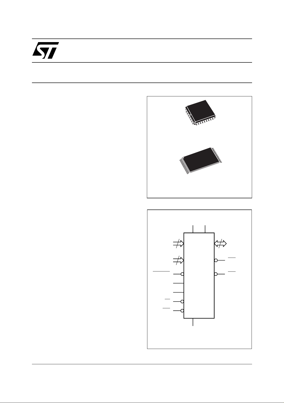
M50LPW041
4 Mbit (512Kb x8, Un iform B lock )
PRELIMINARY DATA
PLCC32 (K)
TSOP40 (N)
10 x 20mm
Figure 1. Logic Diagram (LPC Interface)
V
ID0-ID3
GPI0-
GPI4
LFRAME
CLK
IC
RP
INIT
V
4
5
M50LPW041
V
CC
SS
PP
4
LAD0LAD3
WP
TBL
AI05785
September 2002
This is preliminary information on a new product now in development or undergoing evaluation. Details are subject to change without notice.
1/37
M50LPW041
Figure 2. Logic Diagram (A/A Mux Interface)
V
A0-A10
RC
IC
W
RP
V
11
M50LPW041
G
V
CC
SS
PP
8
DQ0-DQ7
RB
AI05786
DESCRIPTION
The M50LPW041 is a 4 Mbit (512Kb x8) nonvolatile memory that can be read, erased and
reprogrammed. These operations can be
performed using a single low voltage (3.0 to 3.6V)
supply. For fast pro gramming and fast erasing in
production lines an optional 12V power supply can
be used to reduce the programming and the
erasing times.
The memory is divided into blocks that can be
erased independently so it is pos sible to pres erve
valid data while old data is erased. Blocks can be
protected individually to prevent accidental
Program or Erase commands from modifying the
memory. Program and Erase commands are
written to the Command Interface of the m emory.
An on-chip Program/Erase Controller simplifies
the process of programming or erasing the
memory by taking care of all of the special
operations that are required to update the memory
contents. The end of a program or erase operation
can be detected and any error conditions
identified. The command set required to control
the memory is consistent with JEDEC standards.
Two different bus interfaces are supported by t he
memory. The primary interface is the Low Pin
Count (or LPC) Standard Interface. This has been
Figure 3. PLCC Connections
A/A Mux A/A Mux
A7
A6
A5
A4
A3
A2
A1
A0
DQ0
Note: Pins 27 and 28 are not internally connected.
GPI1
GPI0
WP
TBL
ID3
ID2
ID1
ID0
LAD0
GPI2
9
LAD1
DQ1
RPA8VPPV
A9
RP
VPPV
GPI3
1
32
M50LPW041
17
SS
V
V
SS
RFU
LAD3
DQ3
DQ4
LAD2
DQ2
CC
CC
RC
CLK
RFU
DQ5
A10
GPI4
25
RFU
DQ6
IC (VIL)
NC
NC
V
SS
V
CC
INIT
LFRAME
RFU
RFU
IC (VIH)
NC
NC
V
SS
V
CC
G
W
RB
DQ7
A/A MuxA/A Mux
AI05788
2/37
Figure 4. TSOP Connections
M50LPW041
NC
IC (VIH)
NC
NC
NC
NC
A10
NC
RC
V
CC
V
PP
A/A Mux
RP
NC
NC
A9
A8
A7
A6
A5
A4 A3
NC
IC (VIL)
NC
NC INIT
NC RFU
NC
GPI4
NC
CLK
V
CC
V
PP
RP
NC
NC
GPI3
GPI2 LAD0
GPI1 ID0
GPI0
WP
TBL
1
10
M50LPW041
11
20 21
40
31
30
V
V
LFRAME
RFU
RFU
RFU
RFU
V
V
V
LAD3
LAD2
LAD1
ID1
ID2
ID3
SS
CC
CC
SS
SS
V
SS
V
CC
W
G
RB
DQ7
DQ6
DQ5
DQ4
V
CC
V
SS
V
SS
DQ3
DQ2
DQ1
DQ0
A0
A1
A2
A/A Mux
AI06872
designed to remove the need for the ISA bus in
current PC Chipsets; the M50LPW041 acts as the
PC BIOS on the Low P in Count bus for these P C
Chipsets.
The secondary interface, the Address/Address
Multiplexed (or A/A Mux) Int erface, is design ed t o
be compatible with current Flash Programmers for
production line programming prior to fitting to a PC
Motherboard.
The memory is offered in a PLCC32 or TSOP40
(10mm x 20mm) package and is supplied with all
the bits erased (set to 1).
System Memory Mapping
The LPC address sequence is 32 bits long. The
M50LPW041 responds to addresses mapped to
the top of the 4 GByte memory space, from
FFFF FFFFh. Address bits A31-A24 must be set
to 1. A23 is set to 1 for array access, and to 0 for
register access.
The M50LPW041 also responds to addresses
mapped to the bottom of the 4 GByte memory
space, from 0000 0000h. Address bits A31-A24
must be set to 0. A23 is set to 0 for array access,
and to 1 for register access.
For A22-A19, see Table 2. A18-A0 are for array
addresses.
Table 1. Signal Names (LPC Interface) Memory
LAD0-LAD3 Input/Output Communications
LFRAME
ID0-ID3 Identification Inputs
GPI0-GPI4 General Purpose Inputs
IC Interface Configuration
RP
INIT
CLK Clock
TBL
WP
RFU
V
CC
V
PP
V
SS
NC Not Connected Intern ally
Input Communication Frame
Interface Reset
CPU Reset
Top Block Lock
Write Protect
Reserved for Future Use. Leave
disconnected or set at V
Supply Voltage
Optional Supply Voltage for Fast
Erase Operations
Ground
or VIH.
IL
3/37
M50LPW041
SIGNAL DESCRIPTIONS
There are two different bus interfaces available on
this part. The active interface is selected before
power-up or during Reset using the Interface Configur a tion Pin, IC.
The signals for each interface are discussed in the
Low Pin Count (LPC) Signal Descriptions section
and the Address/Address M ultiplexed (A/A Mux)
Signal Descriptions section below. The supply signals are discussed in the Supply S ignal Descriptions section below.
Low Pin Count (LPC) Signal Descriptions
For the Low Pin Count (LPC) Interface see Figure
1, Logic Diagram, and Table 1, Signal Names.
Input/Output Communications (LAD0-LAD3). All
Input and Output Communication with the memory
take place on these pi ns. Addresses and Data for
Bus Read and Bus W rite operations are en coded
on these pins.
Input Communication Frame (LFRAME
Input Communication Frame (LFRAME
). The
) signals
the start of a bus operation. When Input Communication Frame is Low, V
, on the rising edge of
IL
the Clock a new bus operat ion is in itiated. If Input
Communication Frame is L ow, V
, during a bus
IL
operation then the operation is aborted. When Input Communication Frame is High, V
, the cur-
IH
rent bus operation is proceeding or the bus is idle.
Identification Inputs (ID0-ID3). The Identification
Inputs (ID0-ID3) allow to address up to 16
memories on a bus. The value on addresses A19A22 is compared to the hardware strapping on the
ID0-ID3 pins to select which memory is being
addressed, as shown in Table 2.
General Purpose Inputs (GPI0-GPI4). The General Purpose Inputs can be used as digital inputs for
the CPU to read. The General Purpose Input Register holds the values on these pins. The pins must
have stable data from before the start of the cycle
that reads the General Purpose Input Register until after the cycle is complete. These pins must not
be left to float, they should be driven Low, V
High, V
.
IH
IL,
or
Interface Configuration (IC). The Interface Configuration input selects whether the Low Pin Count
(LPC) or the Address/Address Multiplexed (A/A
Mux) Interface is used. The chosen interface must
be selected before power-up or during a Reset
and, thereafter, cannot be change d. The state of
the Interface Configuration, IC, should not be
changed during operation.
Table 2. Memory Identification Input Configuration
Memory
Number
1 (Boot)
2
3
4
5
6
7
8
9
10
11
12
13
14
15
16
ID2 ID2 ID1 ID0
or floating VIL or floating VIL or floating VIL or floating
V
IL
V
or floating VIL or floating VIL or floating V
IL
V
or floating VIL or floating V
IL
V
or floating VIL or floating V
IL
V
or floating V
IL
V
or floating V
IL
V
or floating V
IL
V
or floating V
IL
V
IH
V
IH
V
IH
V
IH
V
IH
V
IH
V
IH
V
IH
IH
IH
IH
IH
VIL or floating VIL or floating VIL or floating
VIL or floating VIL or floating V
VIL or floating V
VIL or floating V
V
IH
V
IH
V
IH
V
IH
IH
IH
VIL or floating VIL or floating
VIL or floating V
V
IH
V
IH
IH
IH
VIL or floating VIL or floating
VIL or floating V
V
IH
V
IH
VIL or floating
VIL or floating
VIL or floating
VIL or floating
Top Bottom
A 22A 21A 20A 19A 22A 21A 20A
11110001
IH
V
IH
IH
V
IH
IH
V
IH
IH
V
IH
11100000
11010011
11000010
10110101
10100100
10010111
10000110
01111001
01101000
01011011
01001010
00111101
00101100
00011111
00001110
19
4/37

M50LPW041
Table 3. System Memory Map
A31:24
Top FFh 1 0
Bottom 00h 0 1
A23
Array Register
To select the Low Pin Count (LPC) Interface the
Interface Configuration pin should be left to float or
driven Low, V
; to select the Address/Address
IL
Multiplexed (A/A Mux) Interface t he pin should be
driven High, V
included with a value of R
current of I
. An internal pull-down resistor is
IH
through each pin when pulled to VIH;
LI2
; there will be a leakage
IL
see Table 21.
Interface Reset (RP
). The Interface Reset (RP)
input is used to reset the memory. When Interface
Reset (RP
) is set Low, VIL, the memor y i s i n R ese t
mode: the outputs are put to high impedance and
the current consumption is minimized. When RP
set High, V
, the memory is in no rmal operat ion.
IH
is
After exiting Reset mode, the memory enters
Read mode.
CPU Reset (INIT
). The CPU Reset, INIT, pin is
used to Reset the memory when the CPU is reset.
It behaves identically to Interface Reset, RP
, and
the internal Reset lin e is the logical OR (elec tric al
AND) of RP
and INIT.
Clock (CLK). The Clock, CLK, input is used to
clock the signals in and out of the Input/Output
Communication Pins, LAD0-LAD3. The Clock
conforms to the PCI specification.
Top Block Lock (TB L
). The Top Block Lock
input is used to pre vent the Top Block (Block 7)
from being chan ged. When Top Block Loc k, TBL
is set Low, V
, Program and Block Erase
IL
operations in the Top Block have no effect,
regardless of the state of the Lock Register. When
Top Block Lock, TBL
, is set High, VIH, the
protection of the Block is determined by the Lock
Register. The state of Top Block Lock, TBL
, does
not affect the protection of the Main Blocks (Blocks
0 to 6).
Top Block Lock, TBL
, must be set prior to a Program or Block Erase operation is initiated and
must not be changed until the operation completes
or unpredictable results may occur. Care should
be taken to avoid unpredictable behavior by
changing TBL
Write Protect (WP
during Program or Erase Suspend.
). The Write Protect input is
used to prevent the Main Blocks (Blocks 0 to 6)
from being changed. W hen Write P rotect, WP
set Low, V
, Program and Block Erase operations
IL
, is
in the Main Blocks have no effect, regardless of
the state of the Lock Register. When Write Protect,
, is se t H i g h , VIH, the protection of the Block is
WP
determined by the Lock Register. The state of
Write Protect, WP
, does not affect the protection of
the Top Block (Block 7).
Write Protect, WP
, must be set prior to a Program
or Block Erase operation is initiated and must not
be changed until the o peration completes or unpredictable results may occur. Care should be taken to avoid unpredictable behavior by changing
WP
during Program or Erase Suspend.
Reserved for Future Use (RFU). These pins do
not have assigned func t ions i n this revision of the
part. They may be left disconnected or driven Low,
, or High, VIH.
V
IL
Address/Address Multiplexed (A/A Mux)
Signal Descriptions
For the Address/Address Multiplexed (A/A Mux)
Interface see Figure 2, Logi c Diagram, and Table
4, Signal Names.
Address Inputs (A0-A10). The Address Inputs
are used to set the Row Address bits (A0-A10) and
the Column Address bits (A11-A18). They are
latched during any bus operation by the Row/ Column Address Select input, RC
.
Data Inputs/Outputs (DQ0-DQ7). The Data Inputs/Outputs hold the data that is written to or read
from the memory. They output the data s tored at
the selected address during a Bus Read operation. During Bus Write operations they represent
the commands sent to the C ommand Interface of
the internal state machine. The Data I nputs/Outputs, DQ0-DQ7, are latched during a Bus Write
operation.
Output Enable (G
). The Output Enable, G, con-
trols the Bus Read operation of the memory.
Write Enable (W
,
the Bus Write operation of the memory’s Com-
). The Write Enable, W, controls
mand Interf a c e .
Row/Column Address Select (RC
). The Row/
Column Address Select input selects whether the
Address Inputs should be latched into the Row
Address bits (A0-A10) or the Column Address bits
(A11-A18). The Row Address bits are latched on
the falling edge of RC
whereas the Column
Address bits are latched on the rising edge.
Ready/Busy Output (RB
). The Ready/Busy pin
gives the status of the memory’s Program/Erase
Controller. When Ready/Busy is Low, V
memory is busy with a Program or Erase operation
and it will not accept any additional Program or
Erase command except the Program/Erase
Suspend command. When Ready/Busy is High,
V
, the memory is ready for any Rea d, Program
OH
or Erase operation.
OL
, the
5/37
M50LPW041
Supply Signal Descriptions
The Supply Signals are the same for both interfaces.
Supply Voltage. The VCC Supply Voltage
V
CC
supplies the power for all operations (Read, Program, Erase etc.).
The Command Interface is disabled when the V
CC
Supply Voltage is less than t he Lockout Voltage,
V
. This prevents Bus Write operations from
LKO
accidentally damaging the da ta during power up,
power down and power surges. If the Program/
Erase Controller is programming or erasing during
this time then the operation aborts and the
memory contents being altered will be invalid.
After V
becomes valid the Command Interface
CC
is reset to Read mode.
A 0.1µF capacitor should be connected betwe en
the V
Supply Voltage pins and t he VSS Ground
CC
pin to decouple the current surges from the power
supply. Both V
Supply Voltage pins must be
CC
connected to the power supply. The PCB track
widths must be sufficient to carry the currents
required during program and erase operations.
Optional Supply Voltage. The VPP Optional
V
PP
Supply Voltage pin is used to select the Fast
Program (see the Quadruple Byte Program
Command desc ription) and F ast Erase options of
the me mor y . V
V
Fast Program (if a Quadruple Byte Program
PPH
can be left floating. When VPP=
PP
Command is performed) and Fast Erase
operations are used.
should not be set to V
V
PP
for more than 80
PPH
hours during the life of the memory.
V
Ground. VSS is the reference for all t he volt-
SS
age measurements.
BUS OPERATIONS
The two interfaces have similar bus operations but
the signals and timings are completely different.
The Low Pin Count (LPC) Interface is the usual
interface and all of t he functionality of the part is
available through this interface. Only a subset of
functions are available through the Address/
Address Multiplexed (A/A Mux) Interface.
Follow the section Low Pin Count (LPC) Bus
Operations below and the section Address/
Address Multiplexed (A/A Mux) Interface Bus
Operations below for a description of the bus
operations on each interface.
Low Pin Count (LPC) Bus Operations
The Low Pin Count (LPC) Interface consists of
four data signals (LAD0-LAD3), one control line
(LFRAME
) and a clock (CLK). In addition
protection against accidental or malicious data
corruption can be achieved using two further
signals (TBL
and WP). Finally two reset signals
Table 4. Signal Names (A/A Mux Interface)
IC Interface Configuration
A0-A10 Address Inputs
DQ0-DQ7 Data Inputs/Outputs
G
W
RC
RB
RP
V
CC
V
PP
V
SS
NC Not Connected Intern ally
Output Enable
Write Enable
Row/Column Address Select
Ready/Busy Output
Interface Reset
Supply Voltage
Optional Supply Voltage for Fast
Program and Fast Erase
Operations
Ground
(RP and INIT) are available to put the memory into
a known state.
The data signals, control signal and clock are
designed to be compatible with PCI electrical
specifications. The interface operates with clock
speeds up to 33MHz.
The following operations can be performed using
the appropriate bus cycles: Bus Read, Bus Write,
Standby, Reset and Block Protection.
Bus Read. Bus Read operations read from the
memory cells, specific registers in the Command
Interface or Low Pin Count Registers. A valid Bus
Read operation starts when Input Communication
Frame, LFRAME
, is Lo w, VIL, as Clock rises and
the correct Start cycle is on LAD0-LAD3. On the
following clock cycles the Host will send the Cycle
Type + Dir, Address and other control bits on
LAD0-LAD3. The memory responds by outputting
Sync data until the wait-states have elapsed
followed by Data0-Data3 and Data4-Data7.
Refer to Table 7, LPC Bus Read Field Definitions,
and Figure 5, LPC Bus Read Waveforms, for a description of the Field definitions for each clock cycle of the transfer. See Table 23, LPC Interface AC
Signal Timing Characteristics and Fi gure 10, LP C
Interface AC Signal Timing Waveforms, for details
on the timings of the signals.
Bus Write. Bus Write operations write to the
Command Interface or Low Pin Count Registers. A
valid Bus Write operation starts when Input
6/37

M50LPW041
Table 5. Absolute Maximum Ratings
Symbol Parameter Value Unit
T
A
T
BIAS
T
STG
(2)
V
IO
V
CC
V
PP
Note: 1. Exc ept for the rating "Operating T em perature R ange", str esses above those listed in the T able "Absol ute Maxim um Ratings " may
cause permanent damage to the device. These are stress ratings only and operation of the device at these or any other conditions
above those indi cated in t he Operating sect i ons of thi s specifi cation i s not impl i ed. Exposure to Absolute M aximum Rating c onditions for extended per iods may aff ect device reliabilit y. Refer also to the STMicroel ectronics SURE Program an d other relevan t qual ity docum en ts .
2. Minimum Vo l tage may undershoot to -2V and for less than 20ns duri ng trans iti ons. Maxim um Voltage may overshoot t o V
and for less th an 20ns duri ng t ransitions.
Ambient Operating Temperature (Temperature Range Option 1) 0 to 70 °C
Temperature Under Bias –50 to 125 °C
Storage Temperature –65 to 150 °C
Input or Output Voltage
Supply Voltage –0.6 to 4 V
Program Voltage –0.6 to 13 V
Communication Frame, LFRAME, is Low, VIL, as
Clock rises and the correct Start cycle is on LAD0LAD3. On the following Clock cycles the Host will
send the Cycle Type + Dir, Add ress, other c ontrol
bits, Data0-Data3 and Data4-Data7 on LAD0LAD3. The memory outputs Sync data until the
wait-states have elapsed.
Refer to Table 8, LPC Bus Write Field Definitions,
and Figure 6, LPC Bus Write Waveforms, for a
description of the Field definitions for each clock
cycle of the transfer. See Table 23, LPC Interface
AC Signal Timing Characteristics and Figure 10,
LPC Interface AC Signal Timing Wa veforms, for
details on the timings of the signals.
Bus Abort. The Bus Abort operation can be used
to immediately abort the current bus operation. A
Bus Abort occurs when LFRAME
V
, during the bus o peration; the m emory wi ll tri-
IL
state the Input/Output Communication pins,
LAD0-LAD3.
Note that, during a Bus Write operation, the
Command Interface starts executing the
command as soon a s the data is f ully received; a
Bus Abort during the final TAR cycles is not
guaranteed to abort the command; the bus,
however, will be released immediately.
Standby. When LFRAME
is High, VIH, the
memory is put into Standb y mode where LA D0LAD3 are put into a high-impedance state and the
Supply Current is reduced to the Standby level,
.
I
CC1
Reset. During Reset mode all internal circuits are
switched off, the memory is deselected and the
outputs are put in high-impedance. The memory is
in Reset mode when Interface Reset, RP
Rese t, IN IT
, is Low, VIL. RP or IN IT must be held
(1)
is driven Low,
, or CPU
Low, V
, for t
IL
–0.6 to V
. The memory resets to Read
PLPH
CC
+ 0.6
V
CC
+2V
mode upon return from Res et mo de and the Lock
Registers return to their default states regardless
of their state before Reset, see Table 16. If RP
INIT
goes Low, VIL, during a Program or Erase
or
operation, the operation is aborted and the
memory cells affected no longer contain valid
data; the memory can take up to t
PLRH
to abort a
Program or Erase operation.
Block Protection. Block Protection can be
forced using the signals Top Block Lock, TBL
Write Protect, WP
, regardless of the state of the
, and
Lock Registers.
Address/Address Multiplexed (A/A Mux) Bus
Operations
The Address/Address Multiplexed (A/A Mux)
Interface has a more traditional style interface.
The signals consist of a multiplexed address
signals (A0-A10), data signals, (DQ0-DQ7) and
three control signals (RC
signal, RP
, can be used to reset the memory.
, G, W). An additional
The Address/Address Multiplexed (A/A Mux)
Interface is included for use by Flash
Programming equipment for faster factory
programming. Only a subset of the features
available to the Low Pin Count (LPC) Interface are
available; these include all the Commands but
exclude the Security features and other registers.
The following operations can be performed using
the appropriate bus cycles: Bus Read, Bus Write,
Output Disable and Reset.
When the Address/Address Multiplexed (A/A Mux)
Interface is selected all the blocks are
unprotected. It is not possible to protect any blocks
through this interface.
7/37
M50LPW041
Table 6. Block Addresses
Size
(Kbytes)
64 70000h-7FFFFh 7 Top Block
64 60000h-6FFFFh 6 Main Block
64 50000h-5FFFFh 5 Main Block
64 40000h-4FFFFh 4 Main Block
64 30000h-3FFFFh 3 Main Block
64 20000h-2FFFFh 2 Main Block
64 10000h-1FFFFh 1 Main Block
64 00000h-0FFFFh 0 Main Block
Note: For A19 value, refer to Table 2.
Address Range
Block
Number
Block Type
Bus Read. Bus Read operations are used to
output the contents of the Memory Array, the
Electronic Signature and the Status Register. A
valid Bus Read operation begins by latching the
Row Address and Column Address signals into
the memory using the Address Inputs, A0-A10,
and the Row/Column Address Select RC
Write Enable (W
be High, V
) and Interface Reset (RP) must
, and Output Enable, G, Low, VIL, in
IH
. Then
order to perform a Bus Read operation. The Data
Inputs/Outputs will output the value, see Figure
12, A/A Mux Interface Read AC Waveforms , and
Table 25, A/A Mux Interface Read AC
Characteristics, for details of when the output
becomes valid.
Bus Write. Bus Write operations write to the
Command Interface. A valid Bus Write operation
begins by latching the Row Address and Column
Address signals into the memory using the
Address Inputs, A0-A10, and the Row/Column
Address Select RC
the Data Inputs/Outputs; Output Enable, G
Interface Reset, RP
Enable, W
, must be Low, VIL. The Data Inputs/
. The data should be set up on
, and
, must be High, VIH and Write
Outputs are latched on the rising edge of Write
Enable, W
. See Figure 13, A/A Mux Interface
Write AC Waveforms, and Table 26, A/A Mux
Interface Write AC Characteristics, for details of
the timing requirements.
Output Disa bl e . The data outputs are high-impedance when the Output Enable, G
, is at VIH.
Reset. During Reset mode all internal circuits are
switched off, the memory is deselected and the
outputs are put in high-impedance. The memory is
in Reset mode when RP
held Low, V
for t
IL
is Low, VIL. RP must be
. If RP is goes Low, VIL,
PLPH
during a Program or Erase operation, the
operation is aborted and the memory cells affected
no longer contain valid data; the memory can take
up to t
to abort a Program or Erase operation.
PLRH
COMMAND INTERFACE
All Bus Write operations to the memory are
interpreted by the Command Interface.
Commands consist of one or more sequential Bus
Write operations.
After power-up or a Reset operation the memory
enters Read mode.
The commands are summarized in Table 12,
Commands. Refer to Tab le 1 2 in conjun ction with
the text descriptions below.
Read Memory A rray Command. The Read Memory Array command returns the memory to its
Read mode where it behaves like a ROM or
EPROM. One Bus Write cycle is required to issue
the Read Memory Array command and return the
memory to Read mode. Once the command is issued the memory remains in Read mode until another command is issued. From Read mode Bus
Read operations will access the memory array.
While the Program/Erase Controller is executing a
Program or Erase operation the m emory will not
accept the Read Memory Array command until the
operation completes.
Read Statu s Registe r Co mm an d . The Read Status Register command is used to read the Status
Register. One Bus Write cycle is required to issue
the Read Status Register command. Once the
command is issued subsequent Bus Read operations read the Status Register until another command is issued. See the section on the Status
Register for details on the definitions of the Status
Register bits.
Read Electronic S i g natu re Comma nd . The Read
Electronic Signature command is used to read the
Manufacturer Code and the Device Code. One
Bus Write cycle is required to issue the Read
Electronic Signature command. Once the
command is issued subsequent Bus Read
operations read the Manufacturer Code or the
Device Code until another command is issued.
After the Read Electronic Signature Command is
issued the Manufacturer Code and Devi ce Code
can be read using Bus Read op erations us ing the
addresses in Table 11.
Program Command. The Program command
can be used to program a value to one address in
the memory array at a time. Two Bus Write
operations are required to issue the command; the
second Bus Write cycle latches the address and
data in the internal state m achine and starts the
Program/Erase Controller. Once the command is
issued subsequent Bus R ead operations read the
Status Register. See the section on the Status
8/37
Table 7. LPC Bus Read Field Definitions
Clock
Cycle
Number
Clock
Cycle
Count
Field
LAD0-
LAD3
Memory
I/O
M50LPW041
Description
1 1 START 0000b I
CYCTY
21
PE +
0100b I
DIR
3-10 8 ADDR XXXX I
11 1 TAR 1111b I
12 1 TAR
1111b
(float)
13-14 2 WSYNC 0101b O
15 1 RSYNC 0000b O
16-17 2 DATA XXXX O
18 1 TAR 1111b O
On the rising edge of CLK with LFRAME
Low, the contents
of LAD0-LAD3 must be 0000b to indicate the start of a LPC
cycle.
Indicates the type of cycle. Bits 3:2 must be 01b. Bit 1
indicates the direction of transfer: 0b for read. Bit 0 is ‘0’.
A 32-bit address phase is transferred starting with the most
significant nibble first. See Tables 3, 2 and 6 for the field
description.
The host drives LAD0-LAD3 to 1111b to indicate a
turnaround cycle.
The LPC Flash Memory takes control of LAD0-LAD3 during
O
this cycle.
The LPC Flash Memory drives LAD0-LAD3 to 0101b (short
wait-sync) for two clock cycles, indicating that the data is not
yet available. Two wait-states are always included.
The LPC Flash Memory drives LAD0-LAD3 to 0000b,
indicating that data will be available during the next clock
cycle.
Data transfer is two CLK cycles, starting with the least
significant nibble.
The LPC Flash Memory drives LAD0-LAD3 to 1111b to
indicate a turnaround cycle.
19 1 TAR
1111b
(float)
Figure 5. LPC Bus Read Waveforms
CLK
LFRAME
LAD0-LAD3
Number of
clock cycles
START
CYCTYPE
+ DIR
1182322
N/A
ADDR TAR SYNC DATA TAR
The LPC Flash Memory floats its outputs, the host takes
control of LAD0-LAD3.
AI04429
9/37
M50LPW041
Table 8. LPC Bus Write Field Definitions
Clock
Cycle
Number
Clock
Cycle
Count
Field
LAD0-
LAD3
Memory
I/O
Description
1 1 START 0000b I
CYCTY
21
PE +
011Xb I
DIR
3-10 8 ADDR XXXX I
11-12 2 DATA XXXX I
13 1 TAR 1111b I
14 1 TAR
1111b
(float)
15 1 SYNC 0000b O
16 1 TAR 1111b O
17 1 TAR
1111b
(float)
N/A
On the rising edge of CLK with LFRAME
Low, the contents
of LAD0-LAD3 must be 0000b to indicate the start of a LPC
cycle.
Indicates the type of cycle. Bits 3:2 must be 01b. Bit 1
indicates the direction of transfer: 1b for write. Bit 0 is don’t
care (X).
A 32-bit address phase is transferred starting with the most
significant nibble first. See Tables 3, 2 and 6 for the field
description.
Data transfer is two cycles, starting with the least significant
nibble.
The host drives LAD0-LAD3 to 1111b to indicate a
turnaround cycle.
The LPC Flash Memory takes control of LAD0-LAD3 during
O
this cycle.
The LPC Flash Memory drives LAD0-LAD3 to 0000b,
indicating it has received data or a command.
The LPC Flash Memory drives LAD0-LAD3 to 1111b,
indicating a turnaround cycle.
The LPC Flash Memory floats its outputs and the host takes
control of LAD0-LAD3.
Figure 6. LPC Bus Write Waveforms
CLK
LFRAME
START
1182212
10/37
LAD0-LAD3
Number of
clock cycles
CYCTYPE
+ DIR
ADDR DATA TAR SYNC TAR
AI04430
Table 9. A/A Mux Bus Operations
Operation G W RP
Bus Read
Bus Write
Output Disable
Reset
V
IL
V
IH
V
IH
V
or V
IL
IH
V
IH
V
IL
V
IH
VIL or V
Table 10. Manufacturer and Device Codes
Operation G
Manufacturer Code
Device Code
V
IL
V
IL
W RP A18-A1 A0 DQ7-DQ0
V
IH
V
IH
M50LPW041
V
PP
V
IH
V
IH
V
IH
IH
V
IL
V
IH
V
IH
Don’t Care Data Output
Float or VCC or V
Don’t Care Hi-Z
Don’t Care Hi-Z
V
IL
V
IL
PPH
V
V
IL
IH
DQ7-DQ0
Data Input
20h
3Ch
Register for details on the definitions of the Status
Register bits.
If the address falls in a pro tected block then the
Program operation will abort, the data in the
memory array will no t be changed and the S tatus
Register will output the error.
During the Program operation the memory will
only accept the Read Status Register command
and the Program/Erase Suspend command. All
other commands will be ignored. Typical Program
times are given in Table 13.
Note that the Program command cannot change a
bit set at ‘0’ back to ‘1’ and attempting to do so will
not cause any modification on its value. One of the
Erase commands must be used to set all of the
bits in the block to ‘1’.
See Figure 14, Program Flowchart and Pseudo
Code, for a suggested flowchart on using the
Program command.
Quadruple Byte Program Command. The Quadruple Byte Program Comman d c an be only used
in A/A Mux mode to program four adjacent bytes
in the memory array at a time. The four bytes must
differ only for the addresses A0 and A1.
Programming should not be attempted when V
is not at V
is below V
if V
PP
. The operation can also be executed
PPH
, but result could be uncertain.
PPH
PP
Five Bus Write operations are required to issue the
command. The second, the third and the fourth
Bus Write cycle latches respectively the address
and data of the first, the second and the third byte
in the internal state machine. The fifth Bus Write
cycle latches the address and data of the fourth
byte in the internal state machine and starts the
Program/Erase Controller. Once the command is
issued subsequent Bus R ead operations read the
Status Register. See the section on the Status
Register for details on the definitions of the Status
Register bits.
During the Quadruple Byte Program operation the
memory will only accept the Read Status register
command and the Program/Erase Suspe nd command. All other commands will be ignored. Typical
Quadruple Byte Program times are given in Table
13.
Note that the Quadruple Byte Program comm and
cannot change a bit set to ‘0’ back to ‘1’ and
attempting to do so will not cause any modification
on its value. One of the Erase commands must be
used to set all of the bits in the block to ‘1’.
See Figure 15, Quadruple Byte Program Flowchart and Pseudo Code, for a suggested flowchart
on using the Quadruple Byte Program command.
Chip Erase Command. The Chip Erase Command can be only used in A/A Mux mode to erase
the entire chip at a time. Erasing should not be attempted when V
can also be executed if V
is not at V
PP
PPH
is b elow V
PP
. The operation
, but re-
PPH
sult could be uncertain. Two Bus Write operations
are required to issue the com mand and start the
Program/Erase Controller. Once the command is
issued subsequent Bus R ead operations read the
Status Register. See the section on the Status
Register for details on the definitions of the Status
Register bits. During the Chip Erase operation the
memory will only accept the Read Status Register
command. All other commands will be ignored.
Typical Chip Erase times are given in T able 13.
The Chip Erase command sets all of the bits in the
memory to ‘1’. See Figure 17, Chip Erase Flowchart and Pseudo Code, for a suggested flowchart
on using the Chip Erase command.
11/37

M50LPW041
Block Erase Command. The Block Erase com-
mand can be used to erase a block. Two Bus Write
operations are required to issue the command; the
second Bus Write cycle latches the block address
in the internal stat e machine and starts th e Program/Erase Controller. Once the command is issued subsequent Bus Read ope rations read the
Status Register. See the section on the Status
Register for details on the definitions of the Status
Register bits.
If the block is protected then the Block Erase
operation will abort, the data in the block will not be
changed and the Status Register will output the
error.
During the Block Erase operation the me mory wi ll
only accept the Read Status Register command
and the Program/Erase Suspend command. All
other commands will be ignored. Typical Block
Erase times are given in Table 13.
The Block Erase command sets all of the bits in
the block to ‘1’. All previous data in the block is
lost.
See Figure 18, Block Erase Flowchart and Pseudo
Code, for a suggested flowchart on using the
Block Erase command.
Clear Status Register Command. The Clear St atus Register command can be used to reset bits 1,
3, 4 and 5 in the Status Register to ‘0’. One Bus
Write is required to issue the Clear Status Register
command. Once the command is issued the memory returns to its previous mode, subs equent Bus
Read operations continue to output the same data.
The bits in the Status Register are stic ky and do
not automatically return to ‘0’ when a new Program
or Erase command is issued. If an error occurs
then it is essential to clear any error bits in the Status Register by issuing the Clear Status Register
command before attempting a new Program or
Erase command.
Program/Erase Suspend Command. The Program/Erase Suspend command can be used to
pause a Program or B lock Erase operation. O ne
Bus Write cycle is required to issue the Program/
Erase Suspend command and pause the Program/Erase Controller. Once the command is issued it is necessary to poll the Program/Erase
Controller Status bit to find out when the Program/
Erase Controller has paused; no other commands
will be accept ed until the Pro gram/ Erase Cont roller has paused. After the Program/Erase Cont roller has paused, the memory will continue to output
the Status Register until another command is issued.
During the polling period between issuing the
Program/Erase Suspend command and the
Program/Erase Controller pausing it is possible for
the operation to complete. Once Program/Erase
Table 11. Read Electronic Signature
Code Address Data
Manufacturer Code 00000h 20h
Device Code 00001h 3Ch
Note: For A19 v al ue, see Tabl e 2.
Controller Status bit indicates that the Program/
Erase Controller is no longer active, the Program
Suspend Status bit or the Erase Suspend Status
bit can be used to d etermine if the opera tion has
completed or is suspended. For timing on the
delay between issuing the Program/Erase
Suspend command and the Program/Erase
Controller pausing see Table 13.
During Program/Erase Suspend the Read
Memory Array, Read Status Register, Read
Electronic Signature and Program/Erase Resume
commands will be accepted by the Command
Interface. Additionally, if the suspe nded operation
was Block Erase then the Program com mand will
also be accepte d; only the blocks no t being erased
may be read or programmed correctly.
See Figures 16, Program Suspend & Resume
Flowchart and Pseudo Code, and 19, Erase
Suspend & Resume Flowchart and Pseudo Code,
for suggested flowcharts on using the Program/
Erase Suspend command.
Program / Erase Resum e Command. The Program/Erase Resume com m and c an be used to restart the Program/Erase Controller after a
Program/Erase Suspend has p aused it. One Bus
Write cycle is required to issue the Program/Erase
Resume command. O nc e the command is iss ued
subsequent Bus Read operations read the Status
Register.
STATUS REGISTER
The Status Register provides information on the
current or previous Program or Erase operation.
Different bits in the Status Register convey
different information and errors on the operation.
To read the Status Register the Read Status
Register command can be issued. The Status
Register is automatically read after Program,
Erase and Program/Erase Resume commands
are issued. The Status Register c an be read from
any address.
The Status Register bits are summarized in Table
14, Status Register Bits. Refer to Table 14 in conjunction with the text descriptions below.
Program/Erase Controller Status (Bit 7). The Progra m/Erase Controller Status bit indicates whether
the Program/Erase Controller is active or inactive.
When the Program/Erase Controller Status bit is
12/37
 Loading...