

SGS Thomson Microelectronics M50FW016 Datasheet
3V Supply Firmware Hub Flash Memory
■ SUPPLY VOLTAGE
= 3 V to 3.6 V for Program, Erase and
–V
CC
Read Operations
–V
= 12 V for Fast Program and Fast Erase
PP
■ TWO INTERFACES
– Firmware Hub (FWH) Interface for embedded
operation with PC Chipsets
– Address/Address Multiplexed (A/A Mux) In-
terface for programm ing equipment compat ibility
■ FIRMWARE HUB (FWH) HARDWARE
INTERFACE MODE
– 5 Signal Communication Interface supporting
Read and Write Operations
– Hardware Write Protect Pins for Block Pro-
tection
– Register Based Read and Write Protection
– 5 Additional Ge neral Pu rpose I nput s f or pla t-
form design flexibility
– Multi-byte Read Operation (4/16/128-byte)
– Synchronized with 33 MHz PCI clock
■ BYTE PROGRAMMING TIME
– Single Byte Mode: 10µs (typical)
– Quadruple Byte Mode: 2.5µs (typical)
■ 32 UNIFORM 64 Kbyte MEMORY BLOCKS
■ PROGRAM and ERASE SUSPEND
– Read other Blocks during Program/Erase
Suspend
– Program other Blocks during Erase Suspend
■ FOR USE in PC BIOS APPLICATIONS
■ ELECTRONIC SIGNATURE
– Manufacturer Code: 20h
– Device Code: 2Eh
M50FW016
16 Mbit (2Mb x8, Uniform Block)
PRELIMINARY DATA
TSOP40 (N)
10 x 20mm
Figure 1. Logi c D iag ram ( FWH I nte rfa ce)
V
ID0-ID3
FGPI0-
FGPI4
FWH4
CLK
IC
RP
INIT
V
4
5
M50FW016
V
CC
SS
PP
4
FWH0FWH3
WP
TBL
AI04462
February 2003
This is preliminary information on a new product now in development or undergoing evaluation. Details are subject to change without notice.
1/37
M50FW016
Figure 2. Logic Diagram (A/A Mux Interface)
V
A0-A10
RC
IC
W
RP
V
11
M50FW016
G
V
CC
SS
PP
8
DQ0-DQ7
RB
AI04463
DESCRIPTION
The M50FW016 is a 16 Mbit (2Mb x8) non-volatile
memory that can be read, erased and
reprogrammed. These operations can be
performed using a single low voltage (3.0 to 3.6V)
supply. For fast programming and fast erasing, an
optional 12V power supply can b e used t o reduce
the programming and the erasing times.
The memory is divided into blocks that can be
erased independently so it is pos sible to pres erve
valid data while old data is erased. Blocks can be
protected individually to prevent accidental
Program or Erase commands from modifying the
memory. Program and Erase commands are
written to the Command Interface of the m emory.
An on-chip Program/Erase Controller simplifies
the process of programming or erasing the
memory by taking care of all of the special
operations that are required to update the memory
contents. The end of a program or erase operation
can be detected and any error conditions
identified. The command set required to control
the memory is consistent with JEDEC standards.
Two different bus interfaces are supported by t he
memory. The primary interface, the Firmware Hub
(or FWH) Interface, uses Intel’s proprietary FWH
protocol. This has been designed to remove the
need for the ISA bus in current PC Chipsets; the
Figure 3. TSOP Connections
NC
IC (VIH)
NC
NC
NC
NC
A10
NC
RC
V
CC
V
PP
A/A Mux
RP
NC
NC
A9
A8
A7
A6
A5
A4 A3
NC
IC (VIL)
NC
NC INIT
NC RFU
NC
FGPI4
NC
CLK
V
CC
V
PP
RP
NC
NC
FGPI3
FGPI2 FWH0
FGPI1 ID0
FGPI0
WP
TBL
1
10
M50FW016
11
20 21
40
31
30
V
SS
V
CC
FWH4
RFU
RFU
RFU
RFU
V
CC
V
SS
V
SS
FWH3
FWH2
FWH1
ID1
ID2
ID3
V
SS
V
CC
W
G
RB
DQ7
DQ6
DQ5
DQ4
V
CC
V
SS
V
SS
DQ3
DQ2
DQ1
DQ0
A0
A1
A2
A/A Mux
AI04464
2/37
M50FW016
M50FW016 acts as the PC BIOS on the Low P in
Count bus for these PC Chipsets.
The secondary interface, the Address/Address
Multiplexed (or A/A Mux) Int erface, is design ed t o
be compatible with current Flash Programmers for
production line programming prior to fitting to a PC
Motherboard.
The memory is offered in TSOP40 (10 x 20mm)
package and it is supplied with all the bits eras ed
(set to ’1’).
SIGNAL DESCRIPTIONS
There are two different bus interfaces available on
this part. The active interface is selected before
power-up or during Reset using the Interface Configur a tion Pin, IC.
The signals for each interface are discussed in the
Firmware Hub (FWH) Signal Descriptions section
and the Address/Address M ultiplexed (A/A Mux)
Signal Descriptions section below. The supply signals are discussed in the Supply S ignal Descriptions section below.
Firmware Hub (FWH) Signal Descriptions
For the Firmware Hub (FWH) Interface see Figure
1, Logic Diagram, and Table 1, Signal Names.
Input/Output Communications (FWH0-FWH3). All
Input and Output Communication with the memory
take place on these pi ns. Addresses and Data for
Bus Read and Bus W rite operations are en coded
on these pins.
Input Communication Frame (FWH4). The Input Communication Frame (FWH4) signals the
start of a bus op eration. When Input Communication Frame is Low, V
, on the rising edge of the
IL
Clock a new bus operation is initiated. If Input
Communication Frame is L ow, V
, during a bus
IL
operation then the operation is aborted. When Input Communication Frame is High, V
, the cur-
IH
rent bus operation is proceeding or the bus is idle.
Identification Inputs (ID0-ID3). The
Identification Inputs select the address that the
memory responds to. Up to 16 memories can be
addressed on a bus. Fo r an address bit to be ‘0’
the pin can be left floating or driven Low, V
IL
; an
internal pull-down resistor is included with a value
. For an address bit to be ‘1’ the pin must be
of R
IL
driven High, V
I
through each pin when pulled to VIH; see Table
LI2
; there will be a leakage current of
IH
20.
By convention the boot memory must have
address ‘0000’ and all additional memories take
sequential addresses starting from ‘0001’.
By convention the boot memory m ust have ID0ID3 pins left floating or driven Low, V
and a ‘1’
IL
value on A21, A23-A25 and all additional
memories take sequential ID0-ID3 configuration.
Table 1. Signal Names (FWH Interface)
FWH0-FWH3 Input/Output Communications
FWH4 Input Communication Frame
ID0-ID3 Identification Inputs
FGPI0-FGPI4 General Purpose Inputs
IC Interface Configuration
RP
INIT
CLK Clock
TBL
WP
RFU
V
CC
V
PP
V
SS
NC Not Connected Intern ally
Interface Reset
CPU Reset
Top Block Lock
Write Protect
Reserved for Future Use. Leave
disconnected.
Supply Voltage
Optional Supply Voltage for Fast
Program and Fast Erase Operations
Ground
General Purpose Inputs (FGPI0-FGPI4) . The General Purpose Inputs can be used as digital inputs
for the CPU to read. Th e General Purpose Input
Register holds the values on t hese pins. The pins
must have stable data f rom before t he s tart of t he
cycle that reads the General Purpose Input Register until after the cycle is complete. These pins
must not be left to float, they should be driven Low,
or High, VIH.
V
IL,
Interface Configuration (IC). The Interface Configuration input selects whether the Firmware Hub
(FWH) or the Address/Address Multiplexed (A/A
Mux) Interface is used. The chosen interface must
be selected before power-up or during a Reset
and, thereafter, cannot be change d. The state of
the Interface Configuration, IC, should not be
changed during operation.
To select the Firmware Hub (FWH) Interface the
Interface Configuration pin should be left to float or
driven Low, V
; to select the Address/Address
IL
Multiplexed (A/A Mux) Interface t he pin should be
driven High, V
included with a value of R
current of I
. An internal pull-down resistor is
IH
through each pin when pulled to VIH;
LI2
; there will be a leakage
IL
see Table 20.
3/37
M50FW016
Table 2. Signal Names (A/A Mux Interface)
IC Interface Configuration
A0-A10 Address Inputs
DQ0-DQ7 Data Inputs/Outputs
G
W
RC
RB
RP
V
CC
V
PP
V
SS
NC Not Connected Intern ally
Output Enable
Write Enable
Row/Column Address Select
Ready/Busy Output
Interface Reset
Supply Voltage
Optional Supply Voltage for Fast
Program and Fast Erase
Operations
Ground
Interface Reset (RP). The Interface Reset (RP)
input is used to reset the memory. When Interface
Reset (RP
) is set Low, VIL, the memor y i s i n R ese t
mode: the outputs are put to high impedance and
the current consumption is minimized. When RP
set High, V
, the memory is in no rmal operat ion.
IH
is
After exiting Reset mode, the memory enters
Read mode.
CPU Reset (INIT
). The CPU Reset, INIT, pin is
used to Reset the memory when the CPU is reset.
It behaves identically to Interface Reset, RP
, and
the internal Reset lin e is the logical OR (elec tric al
AND) of RP
and INIT.
Clock (CLK). The Clock, CLK, input is used to
clock the signals in and out of the Input/Output
Communication Pins, FWH0-FWH3. The Clock
conforms to the PCI specification.
Top Block Lock (TB L
). The Top Block Lock
input is used to prevent the Top Block (Block 31)
from being chan ged. When Top Block Loc k, TBL
is set Low, V
, Program and Block Erase
IL
operations in the Top Block have no effect,
regardless of the state of the Lock Register. When
Top Block Lock, TBL
, is set High, VIH, the
protection of the Block is determined by the Lock
Register. The state of Top Block Lock, TBL
, does
not affect the protection of the Main Blocks (Blocks
0 to 30).
Top Block Lock, TBL
, must be set prior to a Pro-
gram or Block Erase operation is initiated and
must not be changed until the operation completes
or unpredictable results may occur. Care should
be taken to avoid unpredictable behavior by
changing TBL
Write Protect (WP
during Program or Erase Suspend.
). The Write Protect input is
used to prevent the Main Blocks (Blocks 0 to 30)
from being changed. W hen Write P rotect, WP
set Low, V
, Program and Block Erase operations
IL
in the Main Blocks have no effect, regardless of
the state of the Lock Register. When Write Protect,
, is s et High, VIH, the protection of the B lock
WP
determined by the Lock Register. The state of
Write Protect, WP
, does not affect the protection of
the T op Bl ock (Block 31).
Write Protect, WP
, must be set prior to a Program
or Block Erase operation is initiated and must not
be changed until the o peration completes or unpredictable results may occur. Care should be taken to avoid unpredictable behavior by changing
during Program or Erase Suspend.
WP
Reserved for Future Use (RFU). These pins do
not have assigned func t ions i n this revision of the
part. They must be left disconnected.
Address/Address Multiplexed (A/A Mux)
Signal Descriptions
For the Address/Address Multiplexed (A/A Mux)
Interface see Figure 2, Logi c Diagram, and Table
2, Signal Names.
Address Inputs (A0-A10). The Address Inputs
are used to set the Row Address bits (A0-A10) and
the Column Address bits (A11-A20). They are
latched during any bus operation by the Row/ Column Address Select input, RC
.
Data Inputs/Outputs (DQ0-DQ7). The Data Inputs/Outputs hold the data that is written to or read
from the memory. They output the data s tored at
the selected address during a Bus Read operation. During Bus Write operations they represent
the commands sent to the C ommand Interface of
the internal state machine. The Data I nputs/Outputs, DQ0-DQ7, are latched during a Bus Write
operation.
Output Enable (G
). The Output Enable, G, con-
trols the Bus Read operation of the memory.
,
Write Enable (W
). The Write Enable, W, controls
the Bus Write operation of the memory’s Command Interf a c e .
Row/Column Address Select (RC
). The Row/
Column Address Select input selects whether the
Address Inputs should be latched into the Row
Address bits (A0-A10) or the Column Address bits
(A11-A20). The Row Address bits are latched on
the falling edge of RC
whereas the Column
Address bits are latched on the rising edge.
, is
4/37

M50FW016
Table 3. Absolute Maximum Ratings
Symbol Parameter Value Unit
T
A
T
BIAS
T
STG
(2)
V
IO
V
CC
V
PP
Note: 1. Except for the ra ting "Oper at i ng Temperat ure Range", stresse s above th ose listed i n t he Table "Absolute M aximum Rat i ngs" may
cause permanent damage to the device. These are stress ratings only and operation of the device at these or any other conditions
above those indi cated in t he Operating sect i ons of thi s specifi cation i s not impl i ed. Exposure to Absolute M aximum Rating c onditions for extended per iods may aff ect device reliabilit y. Refer also to the STMicroel ectronics SURE Program an d other relevan t qual ity docum en ts .
2. Minimum Voltage may undershoot to –2V, for less than 20 ns, during transitions. Maximum Voltage may overshoot to V
less than 20 ns, during transitions.
Ambient Operating Temperature (Temperature Range Option 1) 0 to 70 °C
Ambient Operating Temperature (Temperature Range Option 5) –20 to 85 °C
Temperature Under Bias –50 to 125 °C
Storage Temperature –65 to 150 °C
Input or Output Voltage
Supply Voltage –0.6 to 4 V
Program Voltage –0.6 to 13 V
Ready/Busy Output (RB). The Ready/Busy pin
gives the status of the memory’s Program/Erase
Controller. When Ready/Busy is Low, V
memory is busy with a Program or Erase operation
and it will not accept any additional Program or
Erase command except the Program/Erase
Suspend command. When Ready/Busy is High,
, the memory is ready for any Rea d, Program
V
OH
or Erase operation.
Supply Signal Descriptions
The Supply Signals are the same for both interfaces.
Supply Voltage. The VCC Supply Voltage
V
CC
supplies the power for all operations (Read, Program, Erase etc.).
The Command Interface is disabled when the V
Supply Voltage is less than the L ockout Voltage,
. This prevents Bus Write operations from
V
LKO
accidentally damaging the data during power up,
power down and power surges. If the Program/
Erase Controller is programming or erasing during
(1)
OL
, the
CC
–0.6 to V
CC
+ 0.6
+2V, for
CC
V
widths must be sufficient to carry the currents
required during program and erase operations.
Optional Supply Voltage. The VPP Optional
V
PP
Supply Voltage pin is used to select the Fast
Program (see the Quadruple Byte Program
Command description) and Fast Erase options of
the memory and to protect the memory. When V
< V
Program and Erase operations cannot be
PPLK
PP
performed and an error is reported in the Sta tus
Register if an attempt to change the memory
contents is made. When V
Erase operations take place as normal. When V
= V
Fast Program operations (using the
PPH
= VCC Program and
PP
PP
Quadruple Byte Program command, 30h, from
Table 13) and Fast Erase operations are used.
Any other voltage input to V
will result in
PP
undefined behavior and should not be used.
V
should not be set to V
PP
for more than 80
PPH
hours during the life of the memory.
V
Ground. VSS is the reference for al l the vol t-
SS
age measurements.
this time then the operation aborts and the
memory contents being altered will be invalid.
After V
becomes valid the Comma nd Interface
CC
is reset to Read mode.
A 0.1µF capacitor should be connected between
the V
Supply Voltage pins and the VSS Ground
CC
pin to decouple the current surges from the power
supply. Both V
Supply Voltage pins must be
CC
connected to the power supply. The PCB track
5/37

M50FW016
Table 4. Block Addresses
Size
(Kbytes)
64 1F0000h-1FFFFFh 31 Top Block
64 1E0000h-1EFFFFh 30 Main Block
64 1D0000h-1DFFFFh 29 Main Block
64 1C0000h-1CFFFFh 28 Main Block
64 1B0000h-1BFFFFh 27 Main Block
64 1A0000h-1AFFFFh 26 Main Block
64 190000h-19FFFFh 25 Main Block
64 180000h-18FFFFh 24 Main Block
64 170000h-17FFFFh 23 Main Block
64 160000h-16FFFFh 22 Main Block
64 150000h-15FFFFh 21 Main Block
64 140000h-14FFFFh 20 Main Block
64 130000h-13FFFFh 19 Main Block
64 120000h-12FFFFh 18 Main Block
64 110000h-11FFFFh 17 Main Block
64 100000h-10FFFFh 16 Main Block
64 0F0000h-0FFFFFh 15 Main Block
64 0E0000h-0EFFFFh 14 Main Block
64 0D0000h-0DFFFFh 13 Main Block
64 0C0000h-0CFFFFh 12 Main Block
64 0B0000h-0BFFFFh 11 Main Block
64 0A0000h-0AFFFFh 10 Main Block
64 090000h-09FFFFh 9 Main Block
64 080000h-08FFFFh 8 Main Block
64 070000h-07FFFFh 7 Main Block
64 060000h-06FFFFh 6 Main Block
64 050000h-05FFFFh 5 Main Block
64 040000h-04FFFFh 4 Main Block
64 030000h-03FFFFh 3 Main Block
64 020000h-02FFFFh 2 Main Block
64 010000h-01FFFFh 1 Main Block
64 000000h-00FFFFh 0 Main Block
Address Range
Block
Number
Block Type
BUS OPERATIONS
The two interfaces have similar bus operations but
the signals and tim ings are compl etely different.
The Firmware Hub (FWH) Interface is the usual
interface and all of the functionality of the part is
available through this in terface. Only a subset of
functions are available through the Address/
Address Multiplexed (A/A Mux) Interface.
Follow the section Firmware Hub (FWH) Bus
Operations below and the section Address/
Address Multiplexed (A/A Mux) Interface Bus
Operations below for a description of the bus
operations on each interface.
Firmware Hub (FWH) Bus Operations
The Firmware Hub (FWH) Interface consists of
four data signals (FWH0-FWH3), one cont rol line
(FWH4) and a clock (CLK). In addition protect ion
against accidental or malicious data corruption
can be achieved using two further signals (TBL
and WP). Finally two reset signals (RP and INIT )
are available to put the memory into a known
state.
The data signals, control signal and clock are
designed to be compatible with PCI electrical
specifications. The interface operates with clock
speeds up to 33MHz.
The following operations can be performed using
the appropriate bus cycles: B us Read, Bus Write,
Standby, Reset and Block Protection.
Bus Read. Bus Read operations read from the
memory cells, specific registers in the Command
Interface or Firmware Hub Reg isters. A valid B us
Read operation starts when Input Communication
Frame, FWH4, is Low, V
, as Clock rises and the
IL
correct Start cycle is on FWH0-FWH3. On the
following clock cycles the Host will send the
Memory ID Select, Address and other control bits
on FWH0-FWH3. The memory responds by
outputting Sync data until the wait-states have
elapsed followed by Data0-Data3 and Data4Data7.
Refer to Table 5, FWH Bus Read Field Definitions,
and Figure 4, FWH Bus Read W avef orms (Sin gle
Byte Read), for a description of the F ield definitions for each clock cycle of the transfer. See Table 22, FWH Interface AC Signal Timing
Characteristics and Figure 10, FWH Interface AC
Signal Timing Waveforms, for details on the timings of the signals.
FWH Bus Write. Bus Write operations write to
the Command Interface or Firmware Hub
Registers. A valid Bus Write operation starts when
Input Communication Frame, FWH4, is Low, V
IL
as Clock rises and the correct Start cycle is on
FWH0-FWH3. On the following Clock cycles the
Host will send the Memory ID Select, Address,
other control bits, Data0-Data3 and Data4-Data7
,
6/37

M50FW016
on FWH0-FWH3. The memory outputs Sync data
until the wait-states have elapsed.
Refer to Table 6, FWH Bus Write Field Definitions,
and Figure 5, FWH Bus Write Waveforms, for a
description of the Field definitions for each clock
cycle of the transfer. See Table 22, FWH Interface
AC Signal Timing Characteristics and Figure 10,
FWH Interface AC Signal Timing Waveforms, for
details on the timings of the signals.
Bus Abort. The Bus Abort operation can be used
to immediately abort the current bus operation. A
Bus Abort occurs when FWH4 is driven Low, V
IL
during the bus operation; the memo ry will tri-state
the Input/Output Communication pins, FWH0FWH3.
Note that, during a Bus Write operation, the
Command Interface starts executing the
command as soon a s the data is f ully received; a
Bus Abort during the final TAR cycles is not
guaranteed to abort the command; the bus,
however, will be released immediately.
Standby. When F WH4 is High, V
, the me mory
IH
is put into Standby mode where FWH0-FWH3 are
put into a high-impedance state and the Supply
Current is reduced to the Standby level, I
CC1
.
Reset. During Reset mode all internal circuits are
switched off, the memory is deselected and the
outputs are put in high-impedance. The memory is
in Reset mode when Interface Reset, RP
Rese t, IN IT
Low, V
, is Low, VIL. RP or IN IT must be held
, for t
IL
. The memory resets to Read
PLPH
, or CPU
mode upon return from Res et mo de and the Lock
Registers return to their default states regardless
of their state before Reset, see Table 15. If RP
INIT
goes Low, VIL, during a Program or Erase
or
operation, the operation is aborted and the
memory cells affected no longer contain valid
data; the memory can take up to t
PLRH
to abort a
Program or Erase operation.
Block Protection. Block Protection can be
forced using the signals Top Block Lock, TBL
Write Protect, WP
, regardless of the state of the
, and
Lock Registers.
Address/Address Multiplexed (A/A Mux) Bus
Operations
The Address/Address Multiplexed (A/A Mux)
Interface has a more traditional style interface.
The signals consist of a multiplexed address
signals (A0-A10), data signals, (DQ0-DQ7) and
three control signals (RC
signal, RP
, can be used to reset the memory.
, G, W). An additional
The Address/Address Multiplexed (A/A Mux)
Interface is included for use by Flash
Programming equipment for faster factory
programming. Only a subset of the features
available to the Firmware Hub (FWH) Interface are
available; these include all the Commands but
exclude the Security features and other registers.
The following operations can be performed using
the appropriate bus cycles: Bus Read, Bus Write,
Output Disable and Reset.
When the Address/Address Multiplexed (A/A Mux)
Interface is selected all the blocks are
unprotected. It is not possible to protect any blocks
through this interface.
Bus Read. Bus Read operations are used to
output the contents of the Memory Array, the
,
Electronic Signature and the Status Register. A
valid Bus Read operation begins by latching the
Row Address and Column Address signals into
the memory using the Address Inputs, A0-A10,
and the Row/Column Address Select RC
Write Enable (W
be High, V
) and Interface Reset (RP) must
, and Output Enable, G, Low, VIL, in
IH
order to perform a Bus Read operation. The Data
Inputs/Outputs will output the value, see Figure
12, A/A Mux Interface Read AC Waveforms , and
Table 24, A/A Mux Interface Read AC
Characteristics, for details of when the output
becomes valid.
Bus Write. Bus Write operations write to the
Command Interface. A valid Bus Write operation
begins by latching the Row Address and Column
Address signals into the memory using the
Address Inputs, A0-A10, and the Row/Column
Address Select RC
. The data should be set up on
the Data Inputs/Outputs; Output Enable, G
Interface Reset, RP
Enable, W
, must be Low, VIL. The Data Inputs/
, must be High, VIH and Write
Outputs are latched on the rising edge of Write
Enable, W
. See Figure 13, A/A Mux Interface
Write AC Waveforms, and Table 25, A/A Mux
Interface Write AC Characteristics, for details of
the timing requirements.
Output Disa bl e . The data outputs are high-impedance when the Output Enable, G
, is at VIH.
Reset. During Reset mode all internal circuits are
switched off, the memory is deselected and the
outputs are put in high-impedance. The memory is
in Reset mode when RP
held Low, V
for t
IL
is Low, VIL. RP must be
. If RP is goes Low, VIL,
PLPH
during a Program or Erase operation, the
operation is aborted and the memory cells affected
no longer contain valid data; the memory can take
up to t
to abort a Program or Erase operation.
PLRH
. Then
, and
7/37
M50FW016
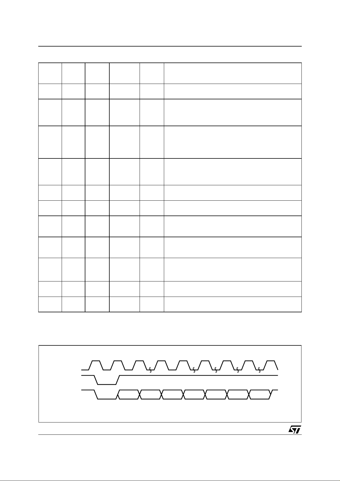
Tabl e 5. FWH Bus Read Field Defin itions
Clock
Cycle
Number
Clock
Cycle
Count
Field
FWH0-
FWH3
Memory
I/O
Description
1 1 START 1101b I
2 1 IDSEL XXXX I
3-9 7 ADDR XXXX I
10 1 MSIZE 0XXXb I
11 1 TAR 1111b I
12 1 TAR
1111b
(float)
13-14 2 WSYNC 0101b O
15 1 RSYNC 0000b O
16-17 2 DATA XXXX O
On the rising edge of CLK with FWH4 Low, the contents of
FWH0-FWH3 indicate the start of a FWH Read cycle.
Indicates which FWH Flash Memory is selected. The value
on FWH0-FWH3 is compared to the IDSEL strapping on the
FWH Flash Memory pins to select which FWH Flash
Memory is being addressed.
A 28-bit address phase is transferred starting with the most
significant nibble first. For the multi-byte read operation, the
least significant bits (MSIZE of them) are treated as Don’t
Care, and the read operation is started with each of these
bits reset to 0.
This one clock cycle is driven by the host to determine how
many bytes will be transferred. M50FW016 will support:
single byte transfer (0000b), 4-byte transfer (0010b), 16-byte
transfer (0100b) and 128-byte transfer (0111b).
The host drives FWH0-FWH3 to 1111b to indicate a
turnaround cycle.
The FWH Flash Memory takes control of FWH0-FWH3
O
during this cycle.
The FWH Flash Memory drives FWH0-FWH3 to 0101b
(short wait-sync) for two clock cycles, indicating that the data
is not yet available. Two wait-states are always included.
The FWH Flash Memory drives FWH0-FWH3 to 0000b,
indicating that data will be available during the next clock
cycle.
Data transfer is two CLK cycles, starting with the least
significant nibble.
enabled, repeat
If multi-byte read operation is
cycle 16-17 n times, where n = 2
MSIZE
–1
Note 1 1 TAR 1111b O
MSIZE
MSIZE
1111b
(float)
–1)*2+18
–1)*2+19
Note 2 1 TAR
Note: 1. Clock Cycle Number = (2
2. Clock Cycle Number = (2
N/A
The FWH Flash Memory drives FWH0-FWH3 to 1111b to
indicate a turnaround cycle.
The FWH Flash Memory floats its outputs, the host takes
control of FWH0-FWH3.
Figure 4. FWH Bus Read Waveforms (Single Byte Read)
CLK
FWH4
START IDSEL ADDR MSIZE TAR SYNC DATA TAR
11712322
8/37
FWH0-FWH3
Number of
clock cycles
AI03437
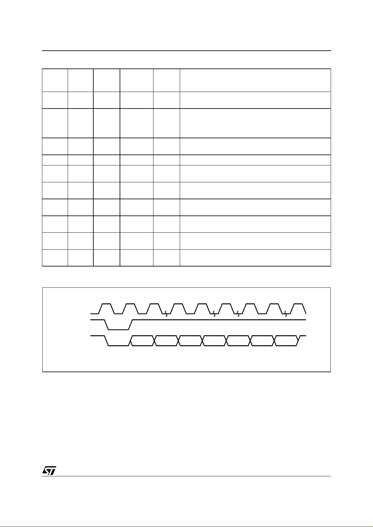
Table 6. FWH Bus Write Field Definitions (Single Byte)
Clock
Cycle
Number
Clock
Cycle
Count
Field
FWH0-
FWH3
Memory
I/O
M50FW016
Description
1 1 START 1110b I
On the rising edge of CLK with FWH4 Low, the contents of
FWH0-FWH3 indicate the start of a FWH Write Cycle.
Indicates which FWH Flash Memory is selected. The value
2 1 IDSEL XXXX I
on FWH0-FWH3 is compared to the IDSEL strapping on the
FWH Flash Memory pins to select which FWH Flash
Memory is being addressed.
3-9 7 ADDR XXXX I
A 28-bit address phase is transferred starting with the most
significant nibble first.
10 1 MSIZE 0000b I Always 0000b (single byte transfer).
11-12 2 DATA XXXX I
13 1 TAR 1111b I
14 1 TAR
1111b
(float)
15 1 S YNC 0000b O
16 1 TAR 1111b O
17 1 TAR
1111b
(float)
N/A
Data transfer is two cycles, starting with the least significant
nibble.
The host drives FWH0-FWH3 to 1111b to indicate a
turnaround cycle.
The FWH Flash Memory takes control of FWH0-FWH3
O
during this cycle.
The FWH Flash Memory drives FWH0-FWH3 to 0000b,
indicating it has received data or a command.
The FWH Flash Memory drives FWH0-FWH3 to 1111b,
indicating a turnaround cycle.
The FWH Flash Memory floats its outputs and the host takes
control of FWH0-FWH3.
Figure 5. FWH Bus Write Waveforms (Single Byte)
CLK
FWH4
FWH0-FWH3
Number of
clock cycles
START IDSEL ADDR MSIZE DATA TAR SYNC TAR
11712212
AI03441
9/37
M50FW016
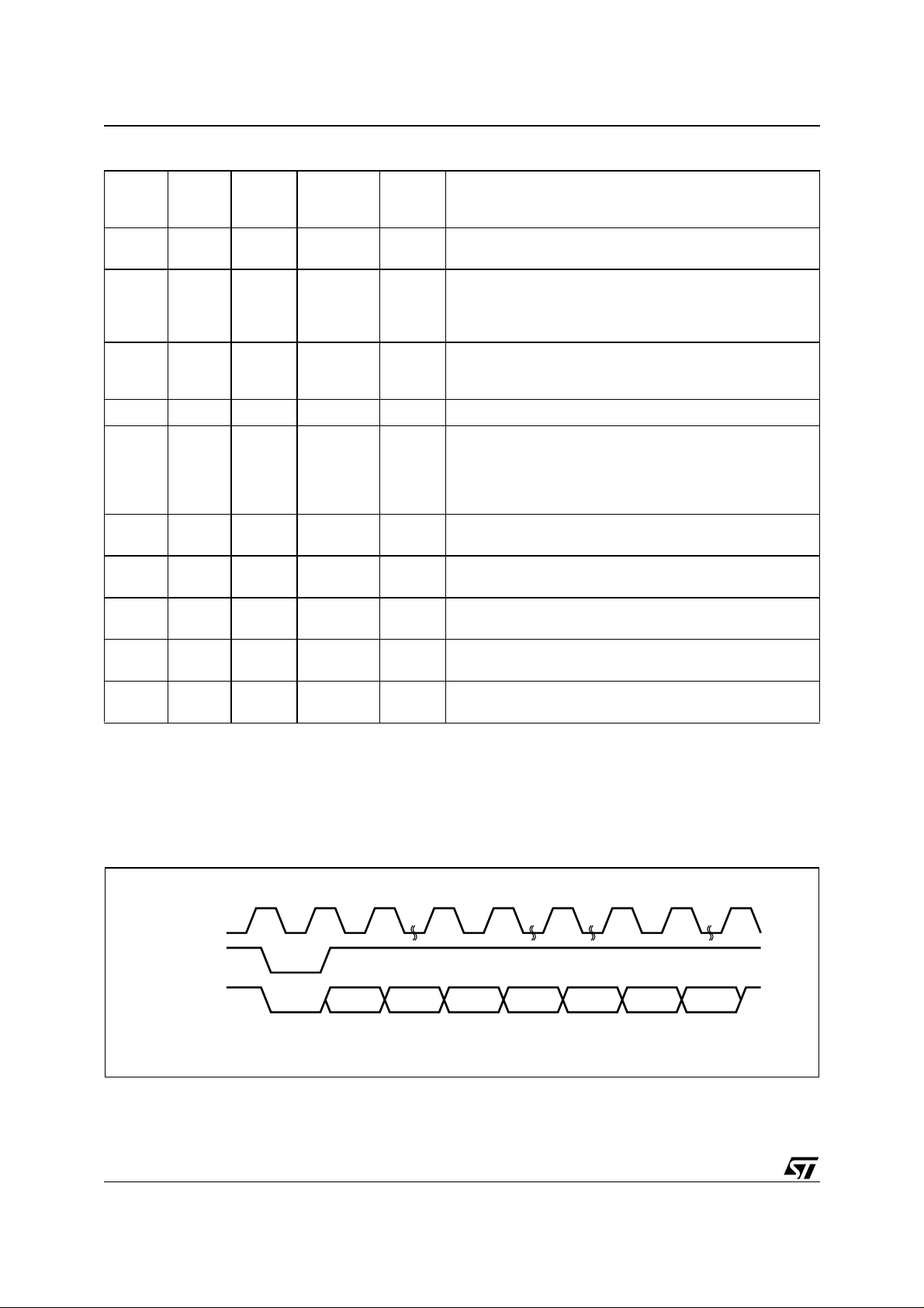
Table 7. FWH Bus Write Field Definitions (Quadruple Byte Program)
Clock
Cycle
Number
Clock
Cycle
Count
Field
FWH0-
FWH3
Memory
I/O
Description
1 1 START 1110b I
On the rising edge of CLK with FWH4 Low, the contents of
FWH0-FWH3 indicate the start of a FWH Write Cycle.
Indicates which FWH Flash Memory is selected. The value
2 1 IDSEL XXXX I
on FWH0-FWH3 is compared to the IDSEL strapping on the
FWH Flash Memory pins to select which FWH Flash
Memory is being addressed.
A 28-bit address phase is transferred starting with the most
3-9 7 ADDR XXXX I
significant nibble first. The A1-A0 lines are treated as Don’t
Care.
10 1 MSIZE 0010b I Always 0010b (quadruple byte transfer).
Data transfer is two cycles, starting with the least significant
nibble. (The first pair of nibbles is that at the address with A1-
11-18 8 DATA XXXX I
A0 set to 00, the second pair with A1-A0 set to 01, the third
pair with A1-A0 set to 10, and the fourth pair with A1-A0 set
to 11.)
19 1 TAR 1111b I
20 1 TAR
1111b
(float)
21 1 S YNC 0000b O
22 1 TAR 1111b O
The host drives FWH0-FWH3 to 1111b to indicate a
turnaround cycle.
The FWH Flash Memory takes control of FWH0-FWH3
O
during this cycle.
The FWH Flash Memory drives FWH0-FWH3 to 0000b,
indicating it has received data or a command.
The FWH Flash Memory drives FWH0-FWH3 to 1111b,
indicating a turnaround cycle.
23 1 TAR
1111b
(float)
N/A
The FWH Flash Memory floats its outputs and the host takes
control of FWH0-FWH3.
Figure 6. FWH Bus Write Waveforms (Quadruple Byte Program)
CLK
FWH4
FWH0-FWH3
Number of
clock cycles
START IDSEL ADDR MSIZE DATA TAR SYNC TAR
11718212
AI05784
10/37
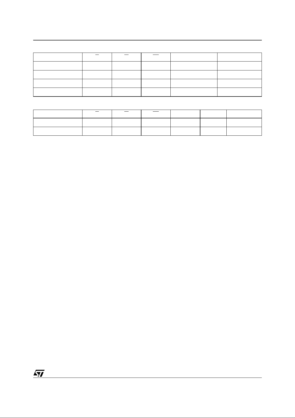
Table 8. A/A Mux Bus Operations
Operation G W RP
Bus Read
Bus Write
Output Disable
Reset
V
IL
V
IH
V
IH
V
or V
IL
IH
V
IH
V
IL
V
IH
VIL or V
Table 9. Manufacturer and Device Codes
Operation G
Manufacturer Code
Device Code
V
IL
V
IL
W RP A20-A1 A0 DQ7-DQ0
V
IH
V
IH
M50FW016
V
PP
V
IH
V
IH
V
IH
IH
V
IL
V
IH
V
IH
Don’t Care Data Output
VCC or V
Don’t Care Hi-Z
Don’t Care Hi-Z
V
V
PPH
IL
IL
V
IL
V
IH
DQ7-DQ0
Data Input
20h
2Eh
COMMAND INTERFACE
All Bus Write operations to the memory are
interpreted by the Command Interface.
Commands consist of one or more sequential Bus
Write operations.
After power-up or a Reset operation the memory
enters Read mode.
The commands are summarized in Table 11,
Commands. Refer to Tab le 1 1 in conjun ction with
the text descriptions below.
Read Memory A rray Command. The Read Memory Array command returns the memory to its
Read mode where it behaves like a ROM or
EPROM. One Bus Write cycle is required to issue
the Read Memory Array command and return the
memory to Read mode. Once the command is issued the memory remains in Read mode until another command is issued. From Read mode Bus
Read operations will access the memory array.
While the Program/Erase Controller is executing a
Program or Erase operation the m emory will not
accept the Read Memory Array command until the
operation completes.
Read Statu s Register Command. The Read Status Register command is used to read the Status
Register. One Bus Write cycle is required to issue
the Read Status Register command. Once the
command is issued subsequent Bus Read operations read the Status Register until another command is issued. See the section on the Status
Register for details on the definitions of the Status
Register bits.
Read Electronic Signature Command. The Read
Electronic Signature command is used to read the
Manufacturer Code and the Device Code. One
Bus Write cycle is required to issue the Read
Electronic Signature command. Once the
command is issued subsequent Bus Read
operations read the Manufacturer Code or the
Device Code until another command is issued.
After the Read Electronic Signature Command is
issued the Manufacturer Code and Devi ce Code
can be read using Bus Read op erations us ing the
addresses in Table 10.
Program Command. The Program command
can be used to program a value to one address in
the memory array at a time. Two Bus Write
operations are required to issue the command; the
second Bus Write cycle latches the address and
data in the internal state m achine and starts the
Program/Erase Controller. Once the command is
issued subsequent Bus R ead operations read the
Status Register. See the section on the Status
Register for details on the definitions of the Status
Register bits.
If the address falls in a pro tected block then the
Program operation will abort, the data in the
memory array will no t be changed and the S tatus
Register will output the error.
During the Program operation the memory will
only accept the Read Status Register command
and the Program/Erase Suspend command. All
other commands will be ignored. Typical Program
times are given in Table 12.
Note that the Program command cannot change a
bit set at ‘0’ back to ‘1’ and attempting to do so will
not cause any modification on its value. One of the
Erase commands must be used to set all of the
bits in the block to ‘1’.
See Figure 14, Program Flowchart and Pseudo
Code, for a suggested flowchart on using the
Program command.
Quadruple Byte Program Command (A/A Mux
Mode). The Q uadruple Byte Program Command
can be used to program four adjacent bytes in the
memory array at a time. The four bytes must differ
only for the addresses A0 a nd A1. Programming
11/37

M50FW016
should not be attempted when VPP is not at V
PPH
Five Bus Write operations are required to issue the
command. The second, the third and the fourth
Bus Write cycle latches respectively the address
and data of the first, the second and the third byte
in the internal state machine. The fifth Bus Write
cycle latches the address and data of the fourth
byte in the internal state machine and starts the
Program/Erase Controller. Once the command is
issued subsequent Bus R ead operations read the
Status Register. See the section on the Status
Register for details on the definitions of the Status
Register bits.
During the Quadruple Byte Program operation the
memory will only accept the Read Status register
command and the Program/Erase Suspe nd command. All other commands will be ignored. Typical
Quadruple Byte Program times are given in Table
12.
Note that the Quadruple Byte Program comm and
cannot change a bit set to ‘0’ back to ‘1’ and
attempting to do so will not cause any modification
on its value. One of the Erase commands must be
used to set all of the bits in the block to ‘1’.
See Figure 15, for a suggested flowchart on using
the Quadruple Byte Program command.
Quadruple Byte Program Command (FWH
Mode). The Q uadruple Byte Program Command
can be used to program four adjacent bytes in the
memory array at a time. The four bytes must differ
only for the addresses A0 a nd A1. Programming
should not be attempted when V
is not at V
PP
PPH
Two Bus Write operations are required to issue the
command. The second Bus Write cycle latches the
start address and four data byt es in the internal
state machine and starts the Program/Erase
Controller. Once the command is issued
subsequent Bus Read operations read the Status
Register. See the section on the Status Register
for details on the definitions of the Status Register
bits.
During the Quadruple Byte Program operation the
memory will only accept the Read Status register
command and the Program/Erase Suspe nd command. All other commands will be ignored. Typical
Quadruple Byte Program times are given in Table
12.
Note that the Quadruple Byte Program comm and
cannot change a bit set to ‘0’ back to ‘1’ and
attempting to do so will not cause any modification
on its value. One of the Erase commands must be
used to set all of the bits in the block to ‘1’.
See Figure 16, for a suggested flowchart on using
the Quadruple Byte Program command.
Chip Erase Command. The Chip Erase Command can be only used in A/A Mux mode to erase
the entire chip at a time. Erasing should not be at-
.
Table 10. Read Electronic Signature
Code Address Data
Manufacturer Code 00000h 20h
Device Code 00001h 2Eh
tempted when V
can also be executed if V
is not at V
PP
PPH
is b elow V
PP
. The operation
sult could be incertain. Two Bus Write operations
are required to issue the com mand and start the
Program/Erase Controller. Once the command is
issued subsequent Bus R ead operations read the
Status Register. See the section on the Status
Register for details on the definitions of the Status
Register bits. During the Chip Erase operation the
memory will only accept the Read Status Register
command. All other commands will be ignored.
Typical Chip Erase times are given in T able 12.
The Chip Erase command sets all of the bits in the
memory to ‘1’. See Figure 18, Chip Erase Flowchart and Pseudo Code, for a suggested flowchart
on using the Chip Erase command.
Block Erase Command. The Block Erase command can be used to erase a block. Two Bus Write
operations are required to issue the command; the
second Bus Write cycle latches the block address
in the internal stat e machine and starts th e Program/Erase Controller. Once the command is issued subsequent Bus Read ope rations read the
Status Register. See the section on the Status
Register for details on the definitions of the Status
.
Register bits.
If the block is protected then the Block Erase
operation will abort, the data in the block will not be
changed and the Status Register will output the
error.
During the Block Erase operation the me mory wi ll
only accept the Read Status Register command
and the Program/Erase Suspend command. All
other commands will be ignored. Typical Block
Erase times are given in Table 12.
The Block Erase command sets all of the bits in
the block to ‘1’. All previous data in the block is
lost.
See Figure 19, Block Erase Flowchart and Pseudo
Code, for a suggested flowchart on using the
Erase command.
Clear Status Register Command. The Clear Status Register command can be used to reset bits 1,
3, 4 and 5 in the Status Register to ‘0’. One Bus
Write is required to issue the Clear Status Register
command. Once the command is issued the memory returns to its previous mode, subs equent Bus
Read operations continue to output the same data.
The bits in the Status Register are stic ky and do
not automatically return to ‘0’ when a new Program
PPH
, but re-
12/37
 Loading...