

Datasheet M48Z2M1Y-70PL1, M48Z2M1Y, M48Z2M1-70PL1, M48Z2M1 Datasheet (SGS Thomson Microelectronics)
16 Mb (2Mb x 8) ZEROPOWER® SRAM
INTEGRATED LOW POWER SRAM,
POWE R-FAIL CONT ROL CIRCUIT and
BATTERIES
CONVENTIONA L SRAM OPERATION;
UNLIMITED W RI TE CYCLE S
10 YEARS of DATA RETENTION in the
ABSENCE of POWER
AUTOMATIC POWER-FAIL CHIP DESELECT
and WRITE PROTECTION
WRITE PROTECT VOLTAGES
= Power-fail Deselect Voltage):
(V
PFD
– M48Z2M1: 4.5V ≤ V
– M48Z2M1Y: 4.2V ≤ V
BA T TERIES A RE INTERNALLY ISOLATED
UNTIL POWER IS APPLIED
PIN and FUNCTION COMPATIBLE with
JEDEC STANDARD 2Mb x 8 SRAMs
PFD
PFD
≤ 4.75V
≤ 4.50V
M48Z2M1
M48Z2M1Y
36
1
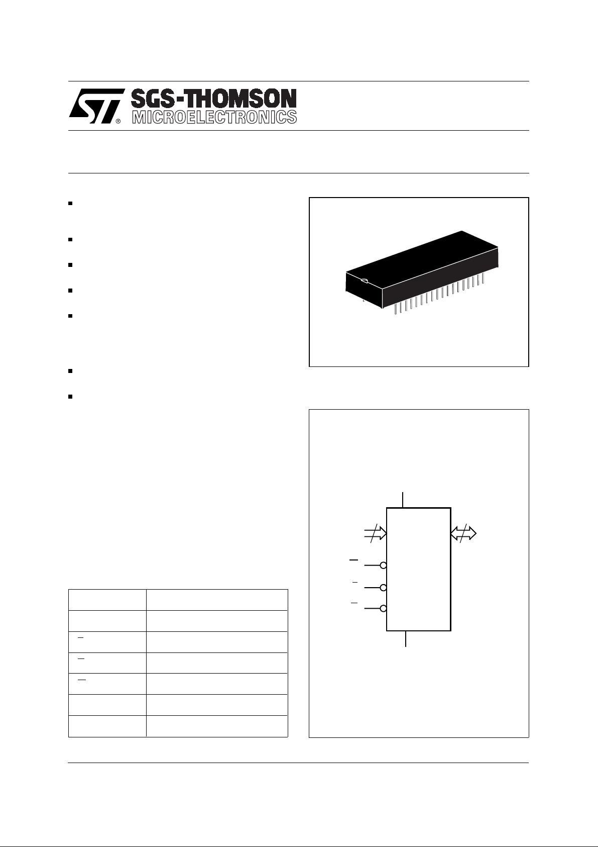
PMLDIP36 (PL)
Module
Figure 1. Logic Diag ra m
DESCRIP TION
®
The M48Z2M1/2M1Y ZEROPOWER
RAM is a
non-volatile 16,777,216 bit Static RAM organized
as 2,097,152 words by 8 bits. The device combines
two internal lithium bat teries, CMO S SRA Ms and a
control circuit in a plastic 36 pin DIP long Module.
The ZEROPOWER RAM replaces industry standard SRAM s. It provides the nonvolatility of P ROMs
without any requirement for special write timing or
limitations on the number of writes that can be
performed.
T able 1. Signal Names
A0-A20 Address Inputs
DQ0-DQ7 Data Inputs / Outputs
E Chip Enable
G Output Enable
W Write Enable
V
CC
V
SS
Supply Voltage
Ground
A0-A20
W
V
CC
21
M48Z2M1
M48Z2M1Y
E
G
V
SS
8
DQ0-DQ7
AI02048
January 1998 1/12
This is preliminary information on a new product now in development or undergoing evaluation. Details are subject to change without notice.
M48Z2M1 , M48Z2M1Y
T ab le 2. Absolut e Maximu m Ra t ings
Symbol Parameter Value Unit
T
A
T
STG
T
BIAS
(2)
T
SLD
V
IO
V
CC
Notes: 1. Stresses greater than those listed under "Absolute Maximum Ratings" may cause permanent damage to the device. This is a
stress rating only and functional operation of the device at these or any other conditions above those indicated in the operational
section of this specification is not implied. Exposure to the absolute maximum rating conditions for extended periods of time may
affect reliability.
2. Soldering temperature not to exceed 260°C for 10 seconds (total thermal budget not to exceed 150°C for longer than 30 seconds).
CAUTION: Negative undershoots below –0.3 volts are not allowed on any pin while in the Battery Back-up mode.
Ambient Operating Temperature 0 to 70 °C
Storage Temperature (VCC Off) –40 to 85 °C
Temperature Under Bias –40 to 85 °C
Lead Soldering Temperature for 10 seconds 260 °C
Input or Output Voltages –0.3 to 7 V
Supply Voltage –0.3 to 7 V
(1)
T ab le 3. Operating Modes
Mode V
Deselect
Write V
Read V
Read V
Deselect V
Deselect ≤ V
Notes: X = VIH or VIL; VSO = Battery Back-up Swit chover V olt age.
CC
4.75V to 5.5V
or
4.5V to 5.5V
to V
SO
(min) X X X High Z CMOS Standby
PFD
SO
E G W DQ0-DQ7 Power
V
IH
IL
IL
IL
X X X High Z Battery Back-up Mode
X X High Z Standby
XVILD
V
IL
V
IH
V
IH
V
IH
IN
D
OUT
High Z Active
Active
Active
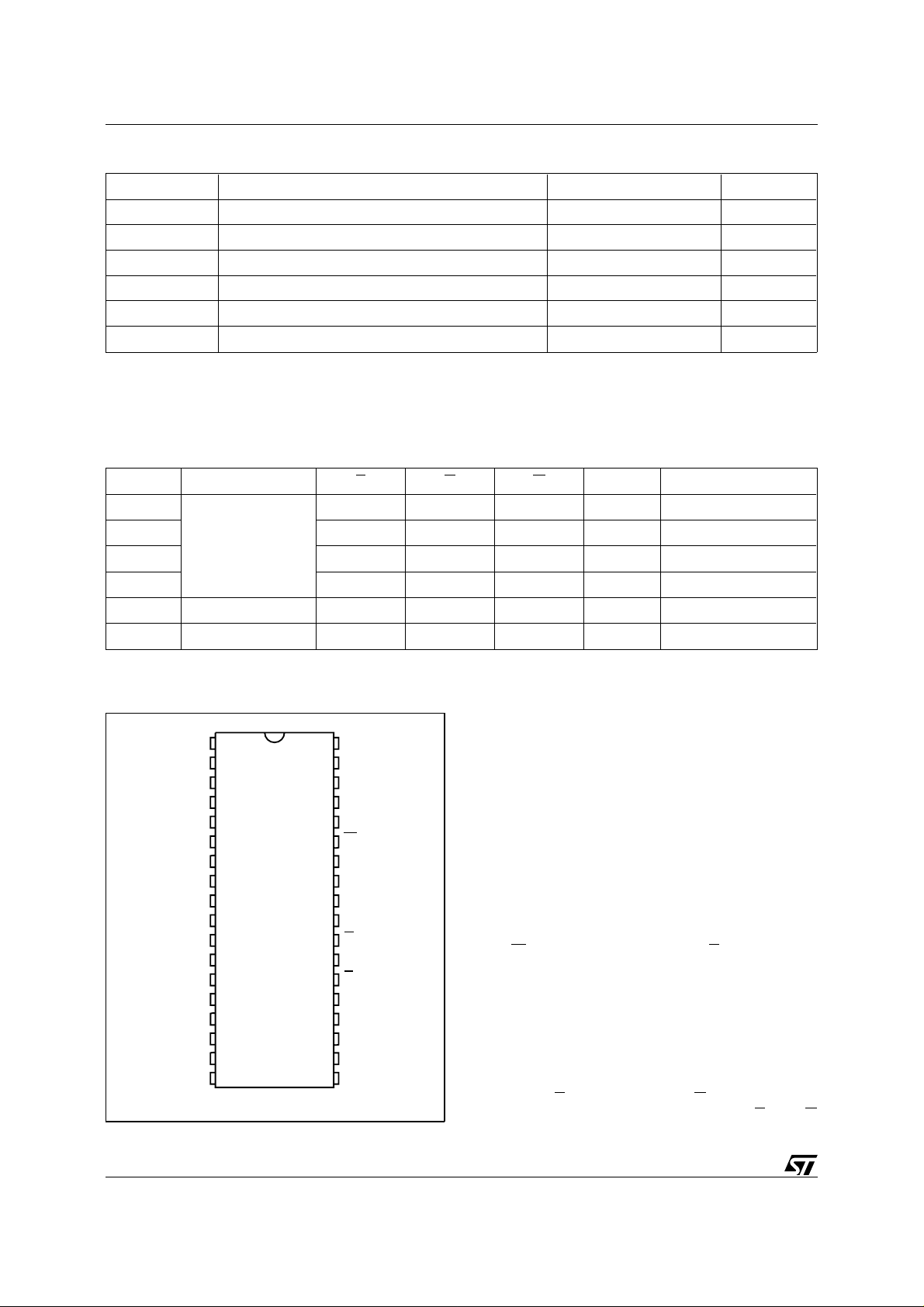
Figure 2. DIP Pin Connection s
1
NC
2
A20
A18
3
A16
4
5
A14
6
A12
A7
7
A6
8
A5
A4
A3
A2
A1
A0
DQ0
M48Z2M1
9
M48Z2M1Y
10
11
12
13
14
15
16
DQ2
17
18
V
SS
Warning: NC = Not Connected.
36
35
34
33
32
31
30
29
28
27
26
25
24
23
22
21
20
19
AI02049
V
CC
A19
NC
A15
A17
W
A13
A8
A9
A11
G
A10
E
DQ7
DQ6
DQ5DQ1
DQ4
DQ3
DESCRIPTION (c ont’d)
The M48Z2M1/2M 1Y has its own Power-fail Detect
Circuit. The cont rol circuitry c onstantly monitors the
single 5V supply for an out of tolerance condition.
When V
is out of tolerance, the circuit write
CC
protects the SRAM, providing a high degree of data
security in the midst of unpredictable system operations brought on by low V
. As VCC falls below
CC
approximately 3V , the control circuitry connects the
batteries which sustain data until valid power returns.
READ MODE
The M48Z2M1/2M1Y is in the Read Mode when -
W (Write Enable) is high and E (Chip E nable)
ever
is low. The device architecture allows ripplethrough access of data from eight of 16,777,216
locations in the static storage array. Thus, the
unique address specified by the 21 Address Inputs
defines which one of the 2,097,152 bytes of data is
to be accessed. Valid data will be available at the
Data I/O pins within Address Access time (t
AVQV
after the last a ddress input signal is stable, provi ding that the
access times are also satisfied. If the
E (Chip Enable) and G (Output Enable)
E and G
access times are not met, valid data will be avail-
)
2/12
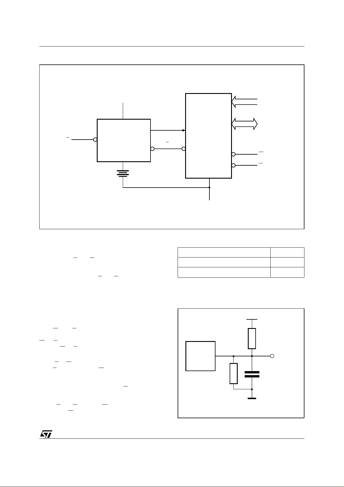
Figure 3. Block Diagram
M48Z2M1, M48Z 2M1 Y
V
CC
A0-A20
POWER
VOLTAGE SENSE
E
AND
SWITCHING
CIRCUITRY
INTERNAL
BATTERIES
able after the later of Chip Enable Access time
) or Output Enable Access Time (t
(t
ELQV
GLQV
). Th e
state of the eight three-state Data I/O signals is
controlled by
before t
indeterminate state until t
puts are changed while
E and G. If the outputs are activated
, the data lines will be driven to an
AVQ V
. If the Address In-
AVQV
E and G remain low, output
data will remain valid for Output Data Hold time
(t
) but will go indeterminate until the next Ad-
AXQX
dress Acc ess.
2048K x 8
SRAM ARRAY
E
V
SS
DQ0-DQ7
W
G
AI02050
Tab le 4. AC Measurement Con ditio ns
Input Rise and Fall Times ≤ 5ns
Input Pulse Voltages 0 to 3V
Input and Output Timing Ref. Voltages 1.5V
Note that Output Hi-Z is defined as the point where data is no
longer driven.
Figure 4. AC T esti ng Load Circui t
WRIT E MO D E
The M48Z2M1/2M1Y is in the Write Mode when-
W and E are active. The start of a write is
ever
referenced from the latter occur ring falling edge of
W or E. A write is terminated by the earlier rising
edge of
W or E.
The addresses must be held valid throughout the
cycle.
E or W must retur n high for minimum of t
from E or t
from W prior to the initiation of
WHAX
EHAX
another read or write cycle. Data-in must be valid
or t
t
DVEH
valid for t
prior to the end of write and remain
DVWH
EHDX
or t
afterward. G should be kept
WHDX
high during write cycles to avoid bus contention;
although, if the output bus has been activated by a
low on
t
E and G, a low on W will disable the outputs
after W falls.
WLQZ
DEVICE
UNDER
TEST
1kΩ
CL includes JIG capacitance
5V
1.9kΩ
OUT
CL = 100pF or 5pF
AI01030
3/12
M48Z2M1 , M48Z2M1Y
T ab le 5. Capacitance
= 25 °C, f = 1 MHz )
(T
A
(1, 2)
Symbol Parameter Test Condition Min Max Unit
C
IN
(3)
C
IO
Notes: 1. Effective capacitance measured with power supply at 5V.
2. Sampled only , not 100% teste d.
3. Outputs deselected
Input Capacitance VIN = 0V 40 pF
Input / Output Capacitance V
= 0V 40 pF
OUT
T ab le 6. DC Characteristics
= 0 to 70°C; VCC = 4.75V to 5.5V or 4.5V to 5.5V)
(T
A
Symbol Parameter Test Condition Min Max Unit
(1)
I
LI
(1)
I
LO
I
Supply Current E = VIL, Outputs open 140 mA
CC
I
CC1
I
CC2
V
IL
V
IH
V
OL
V
OH
Note: 1. Outputs deselected.
Input Leakage Current 0V ≤ VIN ≤ V
Output Leakage Current 0V ≤ V
OUT
≤ V
CC
CC
±4 µA
±4 µA
Supply Current (Standby) TTL E = VIH 10 mA
Supply Current (Standby) CMOS E ≥ VCC – 0.2V 8 mA
Input Low Voltage –0.3 0.8 V
Input High Voltage 2.2 VCC + 0.3 V
Output Low Voltage IOL = 2.1mA 0.4 V
Output High Voltage IOH = –1mA 2.4 V
T ab le 7. Power Down/Up T ri p Points DC Characteri stics
= 0 to 70°C)
(T
A
(1)
Symbol Parameter Min Typ Max Unit
V
PFD
V
PFD
V
SO
t
DR
Notes: 1. All voltages referenced to VSS.
2. At 25°C
Power-fail Deselect Voltage (M48Z2M1) 4.5 4.6 4.75 V
Power-fail Deselect Voltage (M48Z2M1Y) 4.2 4.3 4.5 V
Battery Back-up Switchover Voltage 3 V
(2)
Data Retention Time 10 YEARS
4/12

M48Z2M1, M48Z 2M1 Y
T ab le 8. Power Down/Up Mode AC Characterist ics
= 0 to 70°C)
(T
A
Symbol Parameter Min Max Unit
(1)
t
F
(2)
t
FB
t
WP
t
R
t
ER
Notes:1.V
V
2. V
Figure 5. Power Down/Up Mode AC W avefo rm s
V
(max) to V
PFD
V
(min) to VSO VCC Fall Time 10 µs
PFD
Write Protect Time from VCC = V
VSO to V
PFD
(min) VCC Fall Time 300 µs
PFD
PFD
40 150 µs
(max) VCC Rise Time 0 µs
E Recovery Time 40 120 ms
(max) to V
PFD
passes V
CC
(min) to VSO fall time of less than tFB may cause corruption of RAM data.
PFD
V
CC
V
(max)
PFD
V
(min)
PFD
VSO
(min) fall time of less than tF may result in deselection/write protect ion not occurring until 200 µs after
PFD
(min).
PFD
E
OUTPUTS
tF
tDR
tR
tFB
tWP
DON'T CARE
VALID VALID
(PER CONTROL INPUT)
HIGH-Z
(PER CONTROL INPUT)
tER
RECOGNIZEDRECOGNIZED
AI01031
5/12

M48Z2M1 , M48Z2M1Y
T ab le 9. Read Mode AC Characteristics
= 0 to 70°C; VCC = 4.75V to 5.5V or 4.5V to 5.5V)
(T
A
Symbol Parameter
t
AVAV
t
AVQV
t
ELQV
t
GLQV
t
ELQX
t
GLQX
t
EHQZ
t
GHQZ
t
AXQX
Notes: 1. CL = 100pF (see Figure 4).
2. C
Read Cycle Time 70 ns
(1)
Address Valid to Output Valid 70 ns
(1)
Chip Enable Low to Output Valid 70 ns
(1)
Output Enable Low to Output Valid 35 ns
(2)
Chip Enable Low to Output Transition 5 ns
(2)
Output Enable Low to Output Transition 5 ns
(2)
Chip Enable High to Output Hi-Z 30 ns
(2)
Output Enable High to Output Hi-Z 25 ns
(1)
Address Transition to Output Transition 5 ns
= 5pF (see Figure 4)
L
M48Z2M1 / M48Z2M1Y
-70
Min Max
Unit
Figure 6. Address Cont rolled, Read Mode AC Waveforms
A0-A20
tAVAV
tAVQV
DQ0-DQ7
Note: Chip Enable (E) and Output Enable (G) = Low, Write Enable (W) = High.
tAXQX
DATA VALID
AI02051
6/12

M48Z2M1, M48Z 2M1 Y
Figure 7. Chip Enable or Output Enab le Controlled , Read Mod e AC W avefo r ms
tAVAV
A0-A20
tAVQV tAXQX
tELQV
E
tELQX
tGLQV
G
tGLQX
DQ0-DQ7
Note: Write Enable (W) = High.
DATA R E TE NTION MODE
With valid V
applied, the M48Z2M1/2M1Y oper-
CC
ates as a conventional BYTEWIDE static RAM.
Should the supply voltage decay, the RAM will
automatically power-fail deselect, write protecting
itself t
after VCC falls below V
WP
. All outputs
PFD
become high impedance, and all inputs are treate d
as "don’t care."
If power fail detection occurs during a valid access,
the memory cycle continues to completion. If the
memory cycle fails to terminat e within the time t
write protection takes place. When V
drops be-
CC
WP
VALID
tEHQZ
tGHQZ
DATA OUT
AI02052
low V
, the control circuit switches power to the
SO
internal energy source which preserves data.
The internal coin cells will maintain data in the
M48Z2M1/2M1Y after the initial application of V
for an accumulated period of at least 10 years when
is less than VSO. As sys tem power retur ns and
V
CC
V
rises above VSO, the batteries are discon-
CC
nected, and the power supply is s witc hed to ex ternal Vcc. Writ e protection continues for t
,
reaches V
After t
ER
to allow for processor stabilization.
PFD
, normal RAM operation can resume.
For more information on Battery Storage life refer
to the Application Note AN1012.
after V
ER
CC
CC
7/12

M48Z2M1 , M48Z2M1Y
T ab le 10. W rite M ode AC Ch aracteri stics
= 0 to 70°C; VCC = 4.75V to 5.5V or 4.5V to 5.5V)
(T
A
Symbol Parameter
M48Z2M1 / M48Z2M1Y
-70
Min Max
Unit
t
AVAV
t
AVWL
t
AVEL
t
WLWH
t
ELEH
t
WHAX
t
EHAX
t
DVWH
t
DVEH
t
WHDX
t
EHDX
t
WLQZ
t
AVWH
t
AVEH
t
WHQX
Notes: 1. CL = 5pF (see Figure 4).
2. If
Write Cycle Time 70 ns
Address Valid to Write Enable Low 0 ns
Address Valid to Chip Enable Low 0 ns
Write Enable Pulse Width 55 ns
Chip Enable Low to Chip Enable High 55 ns
Write Enable High to Address Transition 5 ns
Chip Enable High to Address Transition 15 ns
Input Valid to Write Enable High 30 ns
Input Valid to Chip Enable High 30 ns
Write Enable High to Input Transition 0 ns
Chip Enable High to Input Transition 10 ns
(1,2)
Write Enable Low to Output Hi-Z 25 ns
Address Valid to Write Enable High 65 ns
Address Valid to Chip Enable High 65 ns
(1,2)
Write Enable High to Output Transition 5 ns
E goes low simultaneously with W going low, the outputs remain in the high-impedance state.
POWER SUPPLY DECOUPLING and UNDERSHOOT PROT ECTION
transients, including those produced by output
I
CC
switching, can produce voltage fluc tuations, resulting in spikes on the V
bus. These transients can
CC
be reduced if capacitors are used to store energy,
which stabiliz es the V
bus. The energy stored in
CC
the bypass capacitors will be released as low going
spikes are generated or energy will be absorbed
when overshoots occur. A bypass capacitor value
of 0.1µF (as shown in Figure 8) is recommended
in order to provide the needed filtering.
In addition to transients that are c aused by norma l
SRAM operation, power cycling can generate
negative voltage spikes on V
values below V
by as much as one Volt. These
SS
that drive it to
CC
negative spikes can cause data corruption in the
SRAM while in battery backup mode. To protect
from these voltage spikes, it is recommeded to
connect a schottky diode from V
connected to V
, anode to VSS). Schottky diode
CC
to VSS (cathode
CC
1N5817 is recommended for through hole and
MBRS120T3 is recommended for surface mount.
8/12
Figure 8. Supply Voltage Protecti o n
V
CC
V
CC
0.1µF DEVICE
V
SS
AI02169

Figure 9. Write Enabl e Cont rolled , Wri te AC Waveforms
tAVAV
M48Z2M1, M48Z 2M1 Y
A0-A20
tAVEL
E
tAVWL
W
tWLQZ
DQ0-DQ7
Note: Output Enable (G) = High.
VALID
tAVWH
tWLWH
Figure 10. Chip Enabl e Co ntrol led, Wri te AC W avefo r ms
tDVWH
tWHAX
tWHQX
tWHDX
DATA INPUT
AI02053
A0-A20
E
W
DQ0-DQ7
Note: Output Enable (
G) = High.
tAVEL
tAVWL
tAVAV
VALID
tAVEH
tELEH
DATA INPUT
tDVEH
tEHAX
tEHDX
AI02054
9/12

M48Z2M1 , M48Z2M1Y
ORDERI NG INFO RM ATION SCHEM E
Example: M48Z2M1Y -70 PL 1
Supply Voltage and Write
Speed
Package
Temp. Range
Protect Voltage
2M1 VCC = 4.75V to 5.5V
V
= 4.5V to 4.75V
PFD
2M1Y V
Note: 1. Contact Sales Offices for availability of Extended T emperature.
= 4.5V to 5.5V
CC
V
= 4.2V to 4.5V
PFD
-70 70ns
PL PMLDIP36
1 0 to 70°C
(1)
9
Extended
Temperature
For a list of available options (Speed, Package, etc.) or for further information or any aspe ct of this device,
please contact the SGS-THOMSON Sales Office nearest to you.
10/12

M48Z2M1, M48Z 2M1 Y
PMLDIP36 - 36 pin Plastic DIP Long Module
Symb
Typ Min Max Typ Min Max
A 9.27 9.52 0.365 0.375
A1 0.38 – 0.015 –
B 0.43 0.59 0.017 0.023
C 0.20 0.33 0.008 0.013
D 52.58 53.34 2.070 2.100
E 18.03 18.80 0.710 0.740
e1 2.30 2.81 0.090 0.110
e3 38.86 47.50 1.530 1.870
eA 14.99 16.00 0.590 0.630
L 3.05 3.81 0.120 0.150
S 4.45 5.33 0.175 0.210
N36 36
PMLDIP36
mm inches
Drawing is not to scale.
A1AL
S
Be1
eA
C
e3
D
N
E
1
PMDIP
11/12

M48Z2M1 , M48Z2M1Y
Information furnished is b elieved to be accurate and reliable. How ever, SGS-THOMSON Microelectr onics assumes no responsibility for the
consequences of use of such information nor for any infringement of patents or other rights of third parties which may result from its use. No
license is granted by implication or otherwise under any patent or patent rights of SGS-THOMSON Microelectronics. Specificat ions mentioned
in this publication are subject to change without notice. This publication supersedes and replaces all information previously supplied.
SGS-THOMSON Microelectronics products are not authorized for use as critical components in life support devices or systems without express
written approval of SGS-THOMSON Microelectronics.
© 1998 SGS-THOMSON Microelectronics - All Rights Reserved
® ZEROPOWER is a registered trademark of SGS-THOMSON Microelectronics
BYTEWIDE is a trademark of SGS-THOMSON Microelectronics
Australia - Brazil - Canada - China - France - Germany - Italy - Japan - Korea - Malaysia - Malta - Morocco - The Netherlands -
Singapore - Spain - Sweden - Switzerland - Taiwan - Thailand - United Kingdom - U.S.A.
SGS-THOMSON Microelectronics GROUP OF COMPANIES
12/12
 Loading...