

16 Kbit (2Kb x8) TIMEKEEPERSRAM
INTEGRATEDULTRALOW POWERSRAM,
REALTIME CLOCK and POWER-FAIL
CONTROLCIRCUIT
BYTEWIDE RAM-LIKECLOCK ACCESS
BCD CODEDYEAR, MONTH,DAY, DATE,
HOURS,MINUTES and SECONDS
TYPICALCLOCKACCURACY of±1 MINUTE
a MONTH,AT25°C
SOFTWARE CONTROLLEDCLOCK
CALIBRATIONforHIGHACCURACY
APPLICATIONS
AUTOMA TICPOWER-F AILCHIPDESELECTand
WRITEPROTECTIO N
WRITEPROTECT VOLTAGES
= Power-failDeselectVoltage):
(V
PFD
– M48T02: 4.5V≤V
– M48T12: 4.2V≤V
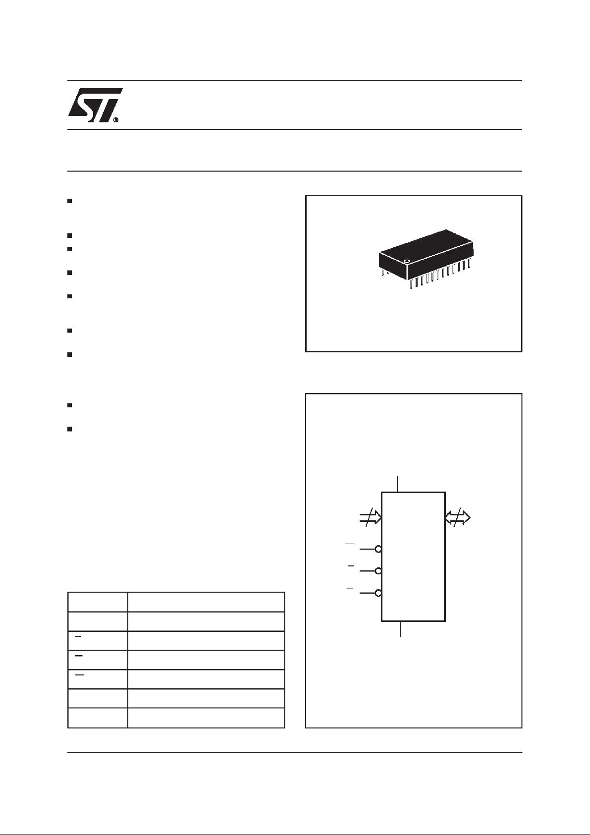
SELF-CONTAINEDBATTERYand CRYSTAL
in the CAPHATDIP PACKAGE
PIN and FUNCTION COMPATIBLEwith
JEDECSTANDARD 2Kb x8 SRAMs
PFD
PFD
≤
≤
4.75V
4.5V
M48T02
M48T12
24
1
PCDIP24 (PC)
Battery/Crystal CAPHAT
Figure1. LogicDiagram
DESCRIPTION
TheM48T02/12TIMEKEEPER
RAMis a 2Kb x8
V
CC
non-volatile static RAM and real time clock which
is pin and functionalcompatiblewith theDS1642.
A special 24 pin 600mil DIP CAPHATpackage
11
A0-A10
8
DQ0-DQ7
housesthe M48T02/12siliconwith a quartzcrystal
and a long life lithium button cell to form a highly
integratedbatterybacked-upmemoryandrealtime
clocksolution.
W
M48T02
M48T12
E
Table1. SignalNames
G
A0-A10 Address Inputs
DQ0-DQ7 Data Inputs / Outputs
E Chip Enable
G Output Enable
W Write Enable
V
CC
V
SS
November 1998 1/15
Supply Voltage
Ground
V
SS
AI01027
M48T02, M48T12
Table2. AbsoluteMaximum Ratings
(1)
Symbol Parameter Value Unit
T
A
T
STG
(2)
T
SLD
V
IO
V
CC
I
O
P
D
Notes: 1. Stresses greater than those listed under ”AbsoluteMaximum Ratings” may cause permanent damage to the device. This is a
stress rating only and functional operation of thedevice at these or any other conditionsabove those indicated in the operational
section of this specification is notimplied.Exposure to theabsolute maximum rating conditions for extended periods of timemay
affect reliability.
2. Soldering temperature not to exceed 260°C for 10 seconds (total thermal budget not to exceed 150°C for longer than 30 seconds).
CAUTION:
Ambient Operating Temperature 0 to 70 °C
Storage Temperature (VCCOff, Oscillator Off) –40 to 85
Lead SolderTemperaturefor 10 seconds 260 °C
Input or Output Voltages –0.3to 7 V
Supply Voltage –0.3to 7 V
Output Current 20 mA
Power Dissipation 1 W
Negativeundershoots below –0.3 volts are not allowed on any pin while inthe Battery Back-up mode.
C
°
Table3. OperatingModes
Mode V
CC
Deselect
Write V
Read V
4.75V to 5.5V
or
4.5V to 5.5V
Read V
to V
Deselect V
SO
Deselect
Notes:X=VIHor VIL;VSO= Battery Back-upSwitchover Voltage.
(min) X X X High Z CMOS Standby
PFD
V
≤
SO
E G W DQ0-DQ7 Power
V
IH
IL
IL
IL
X X High Z Standby
XVILD
V
IL
V
IH
V
IH
V
IH
High Z Active
IN
D
OUT
Active
Active
X X X High Z BatteryBack-up Mode
Figure2. DIPPin Connections
A7
2/15
A6
A5
A4
A3
A2
A1
A0
DQ0
DQ2
SS
1
2
3
4
5
6
7
8
9
10
11
12
M48T02
M48T12
24
23
22
21
20
19
18
17
16
15
14
13
AI01028
V
CC
A8
A9
W
G
A10
E
DQ7
DQ6
DQ5DQ1
DQ4
DQ3V
DESCRIPTION(cont’d)
The M48T02/12 button cell has sufficient capacity
andstoragelifetomaintaindataandclockfunctionality for an accumulatedtime period of at least 10
years in the absence of power over the operating
temperaturerange.
The M48T02/12is a non-volatilepin and function
equivalentto any JEDECstandard 2Kb x8 SRAM.
It also easily fits into many ROM, EPROM, and
EEPROM sockets, providing the non-volatility of
PROMs without any requirement for special write
timing or limitations on the number of writes that
canbe performed.
AsFigure3shows,thestaticmemoryarrayandthe
quartzcontrolledclockoscillatorof the M48T02/12
areintegratedon one silicon chip. The two circuits
are interconnectedat the upper eight memory locations to provide user accessible BYTEWIDE
clockinformationinthebyteswithaddresses7F8h7FFh.The clocklocationscontainthe year,month,
date,day,hour,minute,andsecondin24hourBCD
format.Corrections for 28,29 (leap year), 30, and
31 day months are made automatically.
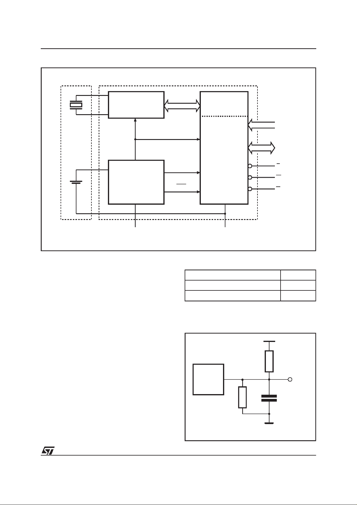
Figure3. Block Diagram
M48T02, M48T12
OSCILLATOR AND
CLOCK CHAIN
32,768
Hz
CRYSTAL
POWER
LITHIUM
CELL
VOLTAGE SENSE
AND
SWITCHING
CIRCUITRY
V
CC
Byte 7F8h is the clock control register. This byte
controlsuser access to the clock information and
also stores the clock calibrationsetting.
The eight clock bytes are not the actual clock
counters themselves; they are memory locations
consisting of BiPORTread/write memory cells.
The M48T02/12 includes a clock control circuit
whichupdatestheclockbyteswithcurrentinformation once per second. The information can be
accessedby the user in the same manner as any
other location in the staticmemory array.
TheM48T02/12also hasits ownPower-failDetect
circuit.Thecontrolcircuitryconstantlymonitorsthe
single 5V supply for an out of tolerancecondition.
When V
is out of tolerance, the circuit write
CC
protectstheSRAM,providingahighdegreeof data
security in the midst of unpredictablesystem operation brought on by low V
.AsVCCfalls below
CC
approximately3V,the controlcircuitryconnectsthe
battery which maintains data and clock operation
until valid powerreturns.
8 x 8 BiPORT
SRAM ARRAY
A0-A10
DQ0-DQ7
E
W
G
V
PFD
BOK
2040 x
SRAM ARRAY
8
V
SS
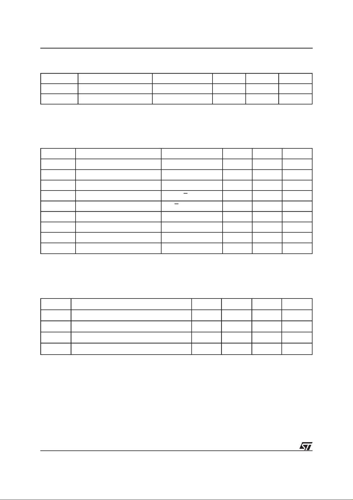
Table4. AC MeasurementConditions
Input Rise and Fall Times
Input Pulse Voltages 0V to 3V
Input and Output TimingRef. Voltages 1.5V
Note that OutputHi-Z is defined as the point where data is no
longer driven.
Figure4. AC TestingLoad Circuit
5V
1.8kΩ
DEVICE
UNDER
TEST
1kΩ
AI01329
5ns
≤
OUT
CL= 100pF
CLincludes JIG capacitance
AI01019
3/15
M48T02, M48T12
Table5. Capacitance
(1)
(TA=25°C, f = 1 MHz )
Symbol Parameter Test Condition Min Max Unit
C
IN
(2)
C
IO
Notes: 1. Effective capacitance measured with power supply at 5V.
2. Outputs deselected.
Input Capacitance VIN=0V 10 pF
Input / Output Capacitance V
=0V 10 pF
OUT
Table6. DC Characteristics
=0 to 70°C; VCC=4.75V to 5.5V or 4.5Vto 5.5V)
(T
A
Symbol Parameter Test Condition Min Max Unit
(1)
I
LI
(1)
I
LO
I
CC
I
CC1
I
CC2
(3)
V
IL
V
IH
V
OL
V
OH
Notes: 1. Outputs Deselected.
2. Measured with Control Bitsset as follows: R = ’1’;W, ST,KS, FT = ’0’.
Input Leakage Current 0V ≤ VIN≤ V
Output Leakage Current 0V ≤ V
OUT
≤ V
CC
CC
Supply Current Outputs open 80 mA
(2)
Supply Current (Standby) TTL E = V
(2)
Supply Current (Standby) CMOS E = VCC– 0.2V 3 mA
IH
Input Low Voltage –0.3 0.8 V
Input High Voltage 2.2 VCC+ 0.3 V
Output Low Voltage IOL= 2.1mA 0.4 V
Output High Voltage IOH= –1mA 2.4 V
±1 µA
±5 µA
3mA
Table7. PowerDown/Up Trip Points DC Characteristics
(1)
(TA=0 to 70°C)
Symbol Parameter Min Typ Max Unit
V
PFD
V
PFD
V
SO
t
DR
Notes: 1. All voltagesreferenced to VSS.
2. At 25°C.
4/15
Power-fail Deselect Voltage (M48T02) 4.5 4.6 4.75 V
Power-fail Deselect Voltage (M48T12) 4.2 4.3 4.5 V
Battery Back-up Switchover Voltage 3.0 V
(2)
Expected Data Retention Time 10 YEARS
M48T02, M48T12
Table8. PowerDown/Up Mode AC Characteristics
=0 to 70°C)
(T
A
Symbol Parameter Min Max Unit
t
PD
(1)
t
F
(2)
t
FB
t
R
t
RB
t
REC
Notes:1.V
2. V
V
E or W at VIHbefore Power Down 0
V
(max) to V
PFD
V
(min) to VSOVCCFall Time 10
PFD
V
(min) to V
PFD
VSOto V
PFD
(min) VCCFall Time 300 µs
PFD
(max) VCCRise Time 0 µs
PFD
(min) VCCRise Time 1
E or W at VIHafter PowerUp 2 ms
(max) to V
PFD
passes V
CC
(min) to VSOfall timeof less than tFBmay cause corruption of RAMdata.
PFD
(min) fall timeof less thantFmay result in deselection/write protection not occurring until 50 µs after
PFD
(min).
PFD
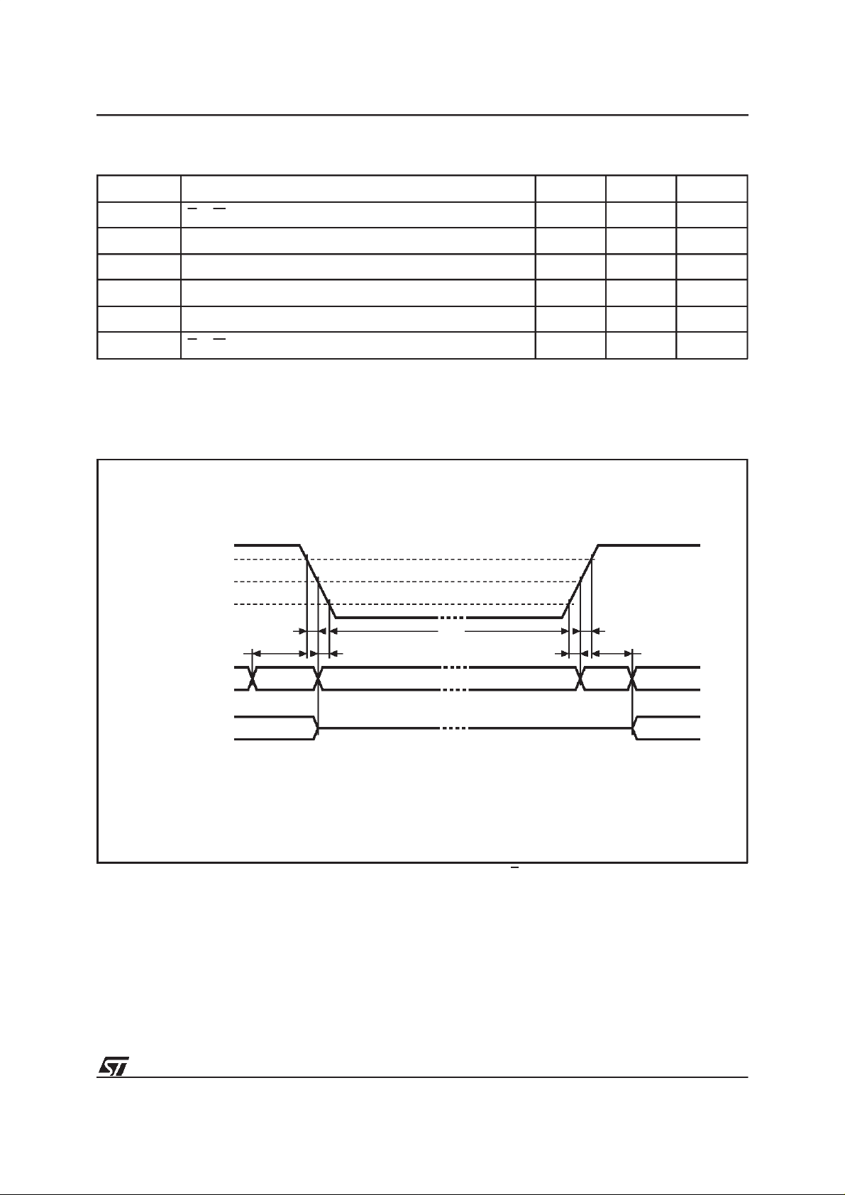
Figure5. Power Down/UpMode AC Waveforms
V
CC
V
(max)
PFD
V
(min)
PFD
V
SO
tF
tFB
INPUTS
tDR
DON’T CARE
NOTE
s
µ
s
µ
s
µ
tR
tRECtPD tRB
RECOGNIZEDRECOGNIZED
OUTPUTS
Note:
Inputs may or may not berecognizedat this time. Caution should betakento keep E high as V
may perform inadvertent write cycles after V
reset is being applied to the processor, a reset conditionmay not occur until after the system clock is running.
VALID VALID
(PER CONTROL INPUT)
rises above V
CC
(min) but before normal system operations begin. Eventhough a power on
PFD
HIGH-Z
rises past V
CC
(PER CONTROL INPUT)
AI00606
(min). Some systems
PFD
5/15
 Loading...