

SGS Thomson Microelectronics M48T08Y Datasheet
5V, 64 Kbit (8 Kb x 8) TIMEKEEPER® SRAM
FEATURES SUMMARY
■ INTEGRATED ULTRA LOW POWER SRAM,
REAL TIME CLOCK, POWER-FAIL CONTROL
CIRCUIT, and BATTERY
■ BYTEWIDE™ RAM-LIKE CLOCK ACCESS
■ BCD CODED YEAR, MONTH, DAY, DATE,
HOURS, MINUTES, and SECONDS
■ TYPICAL CLOCK ACCURACY OF ±1 MINUTE
A MONTH, AT 25°C
■ AUTOMATIC POWER-FAIL CHIP DESELECT
and WRITE PROTECTION
■ WRITE PROTECT VOLTAGES
(V
= Power-fail Deselect Voltage):
PFD
– M48T08: V
4.5V ≤ V
– M48T18/T08Y: V
4.2V ≤ V
■ SOFTWARE CONTROLLED CLOCK
CALIBRATION FOR HIGH ACCURACY
APPLICATIONS
■ SELF-CONTAINED BATTERY and CRYSTAL
IN THE CAPHAT™ DIP PACKAGE
■ PACKAGING INCLU DES A 28-LEAD SOIC and
SNAPHAT
■ (to be Ordered Separately)
■ SOIC PACKAGE PROVIDES DIR EC T
CONNECTION F OR A SNAPHAT TOP WHI CH
CONTAINS THE BATTERY and CRYSTAL
■ PIN and FUNCTION COMPATIBLE WITH
DS1643 and JEDEC STANDARD 8K x 8
SRAMs
= 4.75 to 5. 5V
CC
≤ 4.75V
PFD
≤ 4.5V
PFD
®
TOP
= 4.5 to 5.5V
CC
M48T08
M48T08Y, M48 T18
Figure 1. 28-pin PCDIP, CAPHAT™ Package
28
1
PCDIP28 (PC)
Battery/Crystal
CAPHAT
Figure 2. 28-pi n S O I C Package
SNAPHAT (SH)
Battery/Crystal
28
1
SOH28 (MH)
Rev. 4.0
1/26March 2003

M48T08, M48T18, M48T08Y
TABLE OF CONTENTS
SUMMARY DESCRIPTION. . . . . . . . . . . . . . . . . . . . . . . . . . . . . . . . . . . . . . . . . . . . . . . . . . . . . . . . . . . 3
Figure 3. Logic Diagram . . . . . . . . . . . . . . . . . . . . . . . . . . . . . . . . . . . . . . . . . . . . . . . . . . . . . . . . . . 3
Table 1. Signal Names . . . . . . . . . . . . . . . . . . . . . . . . . . . . . . . . . . . . . . . . . . . . . . . . . . . . . . . . . . . 3
Figure 4. DIP Connections . . . . . . . . . . . . . . . . . . . . . . . . . . . . . . . . . . . . . . . . . . . . . . . . . . . . . . . . 4
Figure 5. SOIC Connections . . . . . . . . . . . . . . . . . . . . . . . . . . . . . . . . . . . . . . . . . . . . . . . . . . . . . . . 4
Figure 6. Block Diagram . . . . . . . . . . . . . . . . . . . . . . . . . . . . . . . . . . . . . . . . . . . . . . . . . . . . . . . . . . 4
MAXIMUM RATING. . . . . . . . . . . . . . . . . . . . . . . . . . . . . . . . . . . . . . . . . . . . . . . . . . . . . . . . . . . . . . . . . 5
Table 2. Absolute Maximum Ratings. . . . . . . . . . . . . . . . . . . . . . . . . . . . . . . . . . . . . . . . . . . . . . . . .5
DC AND AC PARAMETERS. . . . . . . . . . . . . . . . . . . . . . . . . . . . . . . . . . . . . . . . . . . . . . . . . . . . . . . . . . 6
Table 3. Operating and AC Measurement Conditions. . . . . . . . . . . . . . . . . . . . . . . . . . . . . . . . . . . . 6
Figure 7. AC Testing Load Circuit . . . . . . . . . . . . . . . . . . . . . . . . . . . . . . . . . . . . . . . . . . . . . . . . . . . 6
Table 4. Capacitance. . . . . . . . . . . . . . . . . . . . . . . . . . . . . . . . . . . . . . . . . . . . . . . . . . . . . . . . . . . . . 6
Table 5. DC Characteristics. . . . . . . . . . . . . . . . . . . . . . . . . . . . . . . . . . . . . . . . . . . . . . . . . . . . . . . . 7
OPERATION MODES . . . . . . . . . . . . . . . . . . . . . . . . . . . . . . . . . . . . . . . . . . . . . . . . . . . . . . . . . . . . . . . 8
Table 6. Operating Modes. . . . . . . . . . . . . . . . . . . . . . . . . . . . . . . . . . . . . . . . . . . . . . . . . . . . . . . . . 8
READ Mode . . . . . . . . . . . . . . . . . . . . . . . . . . . . . . . . . . . . . . . . . . . . . . . . . . . . . . . . . . . . . . . . . . . 9
Figure 8. READ Mode AC Waveforms . . . . . . . . . . . . . . . . . . . . . . . . . . . . . . . . . . . . . . . . . . . . . . .9
Table 7. READ Mode AC Characteristics . . . . . . . . . . . . . . . . . . . . . . . . . . . . . . . . . . . . . . . . . . . . 10
WRITE Mode. . . . . . . . . . . . . . . . . . . . . . . . . . . . . . . . . . . . . . . . . . . . . . . . . . . . . . . . . . . . . . . . . . 11
Figure 9. WRITE Enable Controlled, WRITE AC Waveform . . . . . . . . . . . . . . . . . . . . . . . . . . . . . .11
Figure 10. Chip Enable Controlled, WRITE AC Waveforms . . . . . . . . . . . . . . . . . . . . . . . . . . . . . . 12
Table 8. WRITE Mode AC Characteristics . . . . . . . . . . . . . . . . . . . . . . . . . . . . . . . . . . . . . . . . . . . 13
Data Retention Mode. . . . . . . . . . . . . . . . . . . . . . . . . . . . . . . . . . . . . . . . . . . . . . . . . . . . . . . . . . . 14
Figure 11. Power Down/Up Mode AC Waveforms . . . . . . . . . . . . . . . . . . . . . . . . . . . . . . . . . . . . . 14
Table 9. Power Down/Up AC Characteristics . . . . . . . . . . . . . . . . . . . . . . . . . . . . . . . . . . . . . . . . .15
Table 10. Power Down/Up Trip Points DC Characteristics . . . . . . . . . . . . . . . . . . . . . . . . . . . . . . . 15
CLOCK OPERATIONS . . . . . . . . . . . . . . . . . . . . . . . . . . . . . . . . . . . . . . . . . . . . . . . . . . . . . . . . . . . . . 16
Reading the Clock. . . . . . . . . . . . . . . . . . . . . . . . . . . . . . . . . . . . . . . . . . . . . . . . . . . . . . . . . . . . . 16
Setting the Clock. . . . . . . . . . . . . . . . . . . . . . . . . . . . . . . . . . . . . . . . . . . . . . . . . . . . . . . . . . . . . . 16
Table 11. Register Map. . . . . . . . . . . . . . . . . . . . . . . . . . . . . . . . . . . . . . . . . . . . . . . . . . . . . . . . . . 16
Stopping and Starting the Oscillator. . . . . . . . . . . . . . . . . . . . . . . . . . . . . . . . . . . . . . . . . . . . . . 17
Calibrating the Clock. . . . . . . . . . . . . . . . . . . . . . . . . . . . . . . . . . . . . . . . . . . . . . . . . . . . . . . . . . . 17
Figure 12. Crystal Accuracy Across Temperature. . . . . . . . . . . . . . . . . . . . . . . . . . . . . . . . . . . . . . 18
Figure 13. Clock Calibration . . . . . . . . . . . . . . . . . . . . . . . . . . . . . . . . . . . . . . . . . . . . . . . . . . . . . . 18
V
Noise And Negative Going Transients. . . . . . . . . . . . . . . . . . . . . . . . . . . . . . . . . . . . . . . . . 19
CC
Figure 14. Supply Voltage Protection . . . . . . . . . . . . . . . . . . . . . . . . . . . . . . . . . . . . . . . . . . . . . . . 19
PACKAGE MECHANICAL INFORMATION . . . . . . . . . . . . . . . . . . . . . . . . . . . . . . . . . . . . . . . . . . . . . 20
PART NUMBERING . . . . . . . . . . . . . . . . . . . . . . . . . . . . . . . . . . . . . . . . . . . . . . . . . . . . . . . . . . . . . . . 24
Table 17. SNAPHAT Battery Table . . . . . . . . . . . . . . . . . . . . . . . . . . . . . . . . . . . . . . . . . . . . . . . . .24
REVISION HISTORY . . . . . . . . . . . . . . . . . . . . . . . . . . . . . . . . . . . . . . . . . . . . . . . . . . . . . . . . . . . . . . . 25
2/26
M48T08, M48T18, M48T08Y
SUMMARY DESCRIPTION
®
The M48T08/18/08Y TIMEKEEPER
RAM is an
8K x 8 non-volatile static RAM and real time clock
which is pin and functional compatible with the
DS1643. The monolithic chip is available in two
special packages to provide a highly integrated
battery backed-up memory and real time clock solution.
The M48T08/18/08Y is a non-volatile pin and function equivalent to any JEDEC standard 8K x 8
SRAM. It also easily fits into many ROM, EPROM,
and EEPROM sockets, providing the non-volatility
of PROMs without any requirement for special
WRITE timing or limitations on the number of
WRITEs that can be performed.
The 28-pin, 600mil DIP CAPHAT™ houses the
M48T08/18/08Y silicon with a quartz crystal and a
long- life lithium button cell in a single package.
The 28-pin, 330mil SOIC provides sockets with
gold plated contacts at both ends for direct connection to a separate SNAPHAT
taining the battery and crystal. The unique design
allows the SNAPHAT battery package to be
mounted on top of the SOIC package after the
completion of the surface mount process. Insertion of the SNAPHAT housing after reflow prevents potential battery and c rystal dam age due to
the high temperatures required for device surfacemounting. The SNAPHAT housing is keyed to prevent reverse insertion.
The SOIC and battery/crystal packages are
shipped separately in plastic anti-static tubes or in
Tape & Reel form. For t he 2 8 le ad S OIC , t he ba ttery/crystal package (e.g., SNAPHAT) part number is “M4T28-BR12SH” or “M4T32-BR12SH”
(see Table 17, page 24).
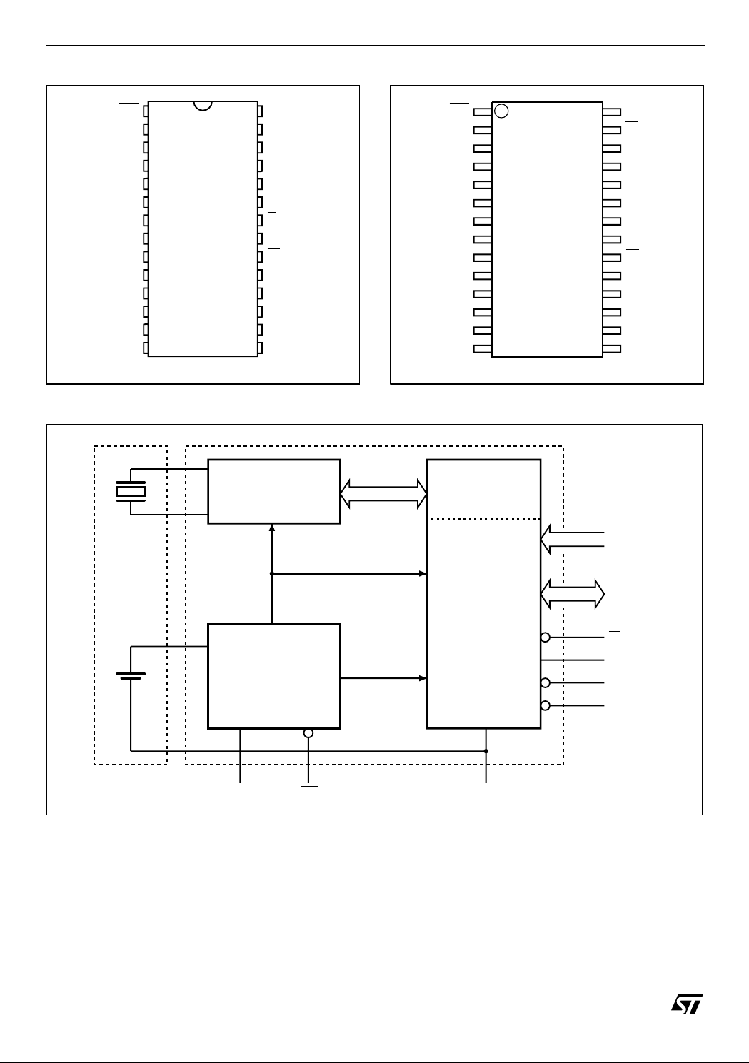
Figure 3. Logic Diagram Table 1. Signal Names
A0-A12 Address Inputs
DQ0-DQ7 Data Inputs / Outputs
INT
E1
Power Fail Interrupt (Open Drain)
Chip Enable 1
A0-A12
13
V
CC
8
DQ0-DQ7
®
housing con-
W
E1 INT
E2
G
M48T08
M48T08Y
M48T18
V
SS
AI01020
E2 Chip Enable 2
G
W
V
V
CC
SS
Output Enable
WRITE Enable
Supply Voltage
Ground
3/26
M48T08, M48T18, M48T08Y
Figure 4. DIP C on ne ctions Figure 5. SOI C Co nn e ct io ns
INT V
1
A12
2
3
A7
4
A6
5
A5
6
A4
7
A3
A2
A1
A0
DQ0
8
9
10
11
M48T08
M48T18
12
13
DQ2
14
SS
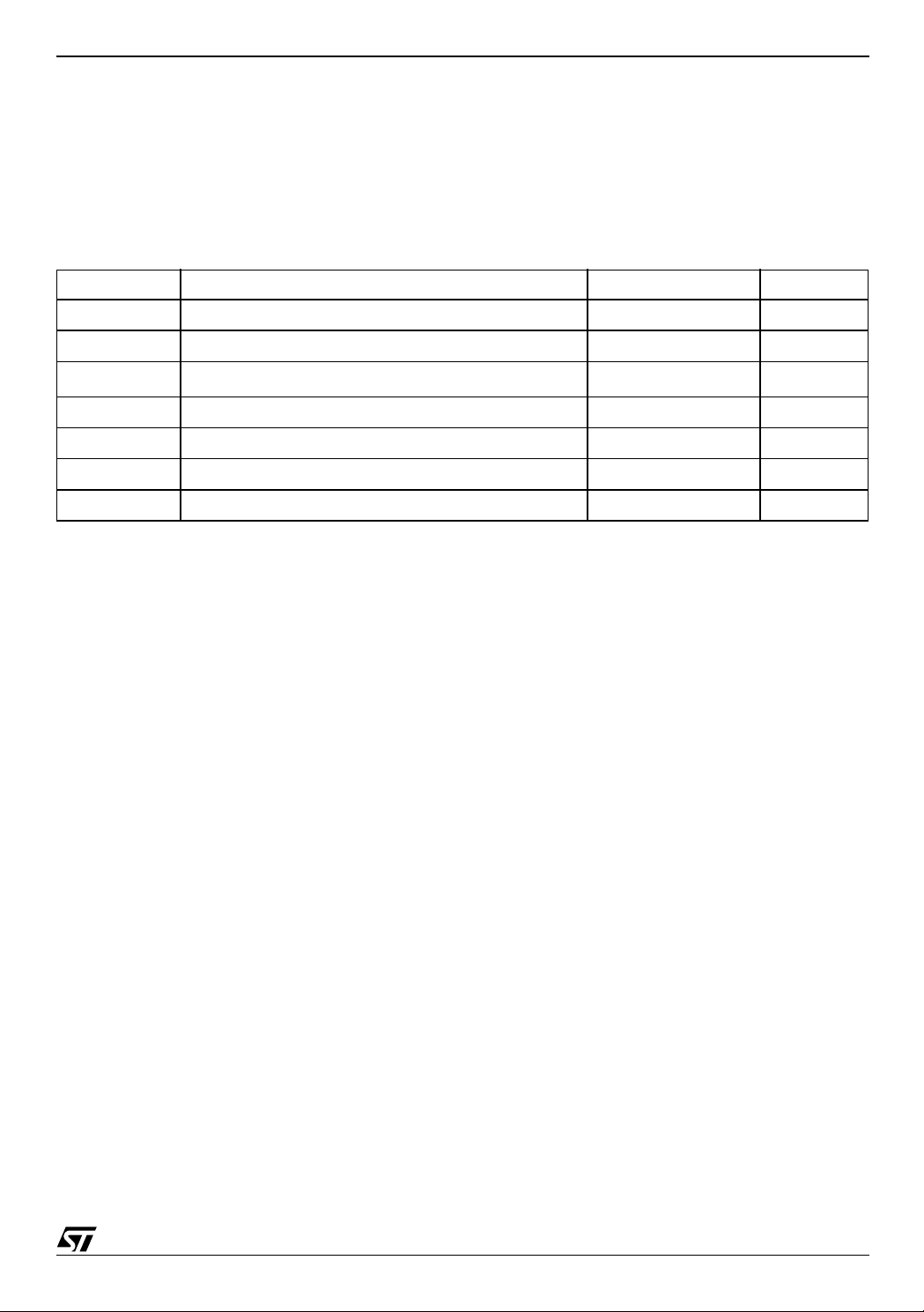
Figure 6. Block Diagram
32,768 Hz
CRYSTAL
28
CC
27
W
26
E2
25
A8
24
A9
23
A11
22
G
21
A10
20
E1
19
DQ7
18
DQ6
17
DQ5DQ1
16
DQ4
15
DQ3V
AI01182
OSCILLATOR AND
CLOCK CHAIN
INT V
A12
A7
A6
A5
A4
A3
A2
A1
A0
DQ0
1
2
3
4
5
6
7
8
9
10
11
M48T08Y
12
DQ2
SS
8 x 8 BiPORT
SRAM ARRAY
13
14
28
27
26
25
24
23
22
21
20
19
18
17
16
15
AI01021B
A0-A12
CC
W
E2
A8
A9
A11
G
A10
E1
DQ7
DQ6
DQ5DQ1
DQ4
DQ3V
LITHIUM
CELL
VOLTAGE SENSE
AND
SWITCHING
CIRCUITRY
CC
INTV
POWER
V
PFD
8184 x 8
SRAM ARRAY
V
SS
DQ0-DQ7
E1
E2
W
G
AI01333
4/26
M48T08, M48T18, M48T08Y
MAXIMUM RATI N G
Stressing the device ab ove the rating listed in t he
“Absolute Maximum Ratings” table may cause
permanent damage to the device. These are
stress ratings only and operation of the dev ice at
these or any other conditions above those indicated in the Operating sections of this specification is
Table 2. Absolute Maximum Ratings
Symbol Parameter Value Unit
T
A
T
STG
(1,2)
T
SLD
V
IO
V
CC
I
O
P
D
Note: 1. For DIP package: Soldering temperature not to exceed 260°C for 10 seconds (total thermal budget not to exceed 150°C for longer
than 30 seco nd s) .
2. For SO pa ck age: Re flow at pea k temp era ture of 2 15°C t o 225° C fo r < 60 se conds (tot al t herm al bu dge t not to excee d 180 °C for
between 90 t o 120 seco nds).
CAUTION: Negative undershoots below –0.3V are not allowed on any pin while in the Battery Back-up mode.
CAUTION: Do NOT wave solder SOIC t o avoid damaging SNAP HAT sockets.
Ambient Operating Temperature 0 to 70 °C
Storage Temperature (VCC Off, Oscillator Off)
Lead Solder Temperature for 10 seconds 260 °C
Input or Output Voltages –0.3 to 7 V
Supply Voltage –0.3 to 7 V
Output Current 20 mA
Power Dissipation 1 W
not implied. Exposure to Absol ute Maxim um Ra ting conditions for extended periods may affect device reliability. Refer also to the
STMicroelectronics SURE Program and other relevant quality documents.
–40 to 85 °C
5/26
M48T08, M48T18, M48T08Y
DC AND AC PARAMETERS
This section summarizes the operat ing and measurement conditions, as well as the DC and AC
characteristics of the device. The parameters in
the following DC and AC Characteristic tables are
derived from tests performed under the M easure-
Table 3. Operating and AC Measurement Conditions
Parameter M48 T08 M48T18/T08Y Unit
ment Conditions listed in the rel evant tables. Designers should check that the operating conditions
in their projects match the measurement conditions when using the quoted parameters.
Supply Voltage (V
Ambient Operating Temperature (T
Load Capacitance (C
CC
)
)
A
)
L
4.75 to 5.5 4.5 to 5.5 V
0 to 70 0 to 70 °C
100 100 pF
Input Rise and Fall Times ≤ 5 ≤ 5ns
Input Pulse Voltages 0 to 3 0 to 3 V
Input and Output Timing Ref. Voltages 1.5 1.5 V
Note: Output Hi-Z is defined as the point wh ere data is no l onger driv en.
Figure 7. AC Testing Load Circuit
5V
1.8kΩ
DEVICE
UNDER
TEST
1kΩ
OUT
CL = 100pF
CL includes JIG capacitance
AI01019
Table 4. Capacitance
Symbol
C
IN
C
IO
Note: 1. Effecti ve capacit ance meas ured with po wer supp l y at 5V ; sampled only, not 100% tested.
2. At 25°C, f = 1MHz.
3. Outputs desele ct ed.
Input Capacitance 10 pF
(3)
Input / Output Capacitance 10 pF
Parameter
6/26
(1,2)
Min Max Unit
Table 5. DC Characteristics
Symbol Parameter
Test Condition
(1)
M48T08, M48T18, M48T08Y
M48T08/M48T18/T08Y
Unit
Min Max
I
LI
(2)
I
LO
I
CC
(3)
I
CC1
(3)
I
CC2
(4)
V
IL
V
IH
Input Leakage Current
Output Leakage Current
Supply Current Outputs open 80 mA
Supply Current (Standby) TTL
Supply Current (Standby) CMOS
Input Low Voltage –0.3 0.8 V
Input High Voltage 2.2
0V ≤ V
0V ≤ V
E1
E1
E2 = V
Output Low Voltage
V
OL
Output Low Voltage (INT
V
OH
Note: 1. Valid for Ambien t Operating T em perature: TA = 0 to 70°C; VCC = 4.75 to 5.5V or 4.5 to 5.5V ( except whe re noted).
2. Outputs desele ct ed.
3. Measured with Control Bits set as follows: R = '1'; W, ST, FT = '0.'
4. Negative s p i k e s of –1V allo wed for up t o 10 ns once pe r Cycle.
5. The INT
Output High Voltage
pin is Open Drain.
(5)
)
≤ V
IN
CC
≤ V
OUT
= V
E2 = V
IH,
= VCC – 0.2V,
+ 0.2V
SS
I
= 2.1mA
OL
IOL = 0.5mA
I
= –1mA
OH
CC
±1 µA
±1 µA
IL
3mA
3mA
V
+ 0.3
CC
0.4 V
0.4 V
2.4 V
V
7/26
M48T08, M48T18, M48T08Y
OPERATION MODES
As Figure 6, page 4 s hows, the static memory array and the quartz-controlled clock oscillator of the
M48T08/18/08Y are integrated on one silicon chip.
The two circuits are interconnected at the upper
eight memory locations to provide user accessible
BYTEWIDE™ clock information in the by tes with
addresses 1FF8h-1FFFh.
The clock locations contain the year, month, date,
day, hour, minute, and second in 24 hour BCD format. Corrections for 28, 29 (leap yea r - valid until
2100), 30, and 31 day months are made automatically. Byte 1FF8h is the clock control register. This
byte controls user access to the clock information
and also stores the clock calibration setting.
The eight clock bytes are not the actual clock
counters themselves; they are memory locat ions
consisting of BiPORT™ READ/WRITE memory
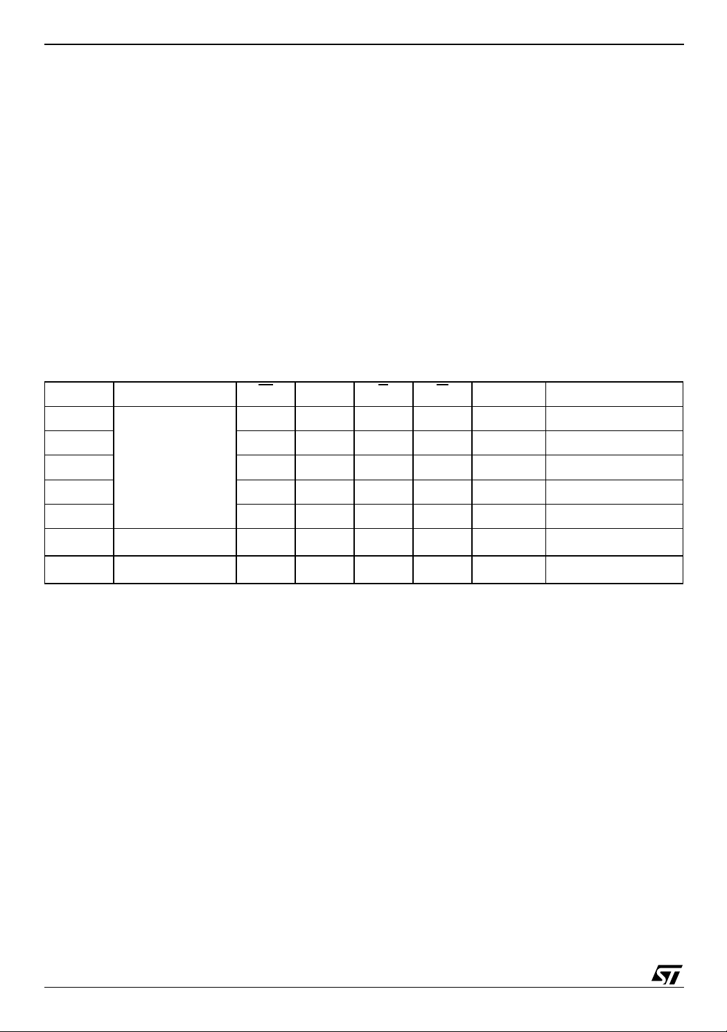
Table 6. Operating Modes
4.75 to 5.5V
4.5 to 5.5V
VSO to V
≤ V
V
CC
or
PFD
SO
(min)
(1)
(1)
E1 E2 G W DQ0-DQ7 Power
V
IH
V
IL
V
IL
V
IL
X X X X High Z CMOS Standby
X X X X High Z Battery Back-up Mode
X X X High Z Standby
V
IL
V
IH
V
IH
V
IH
Mode
Deselect
Deselect X
WRITE
READ
READ
Deselect
Deselect
Note: X = VIH or VIL; VSO = Batte ry Back -up Swit c h over Vol tage.
1. See Table 10, page 15 for detail s.
cells. The M48T08/18/08Y includes a clock control
circuit which updates the clock bytes with current
information once per second. The information can
be accessed by the user in the same manner as
any other location in the static memory array.
The M48T08/18/08Y also has its own Power-fail
Detect circuit. The control circuitry constantly monitors the single 5V supply for an out of tolerance
condition. When V
is out of tolerance, the circuit
CC
write protects the S RAM, p roviding a high degree
of data security in the midst of unpredictable s ystem operation brought on by low V
. As VCC falls
CC
below the Battery Back-up Switchover Voltage
), the control circuitry connects the battery
(V
SO
which maintains data and clock operation until valid power returns.
X X High Z Standby
X
V
IL
V
IH
V
IL
V
IH
V
IH
D
IN
D
OUT
High Z Active
Active
Active
8/26
 Loading...