

512 Bit (64 bit x8) SERIAL RTC (SPI) SRAM
FEATURES SUMMARY
■ 2.7 TO 5.5V OPERATING V OLT AGE
■ SERIAL PERIPHERAL INTERFACE (SPI)
■ 2.5 TO 5.5V OSCILLATOR OPERATING
VOLTAGE
■ AUTOMATIC SWITCH-OVER and DESELECT
CIRCUITRY
■ CHOICE OF POWER-FAIL DESELECT
VOLTAGES (V
–THS = V
–THS = V
■ COUNTERS FOR TENTHS/HUNDREDTHS
OF SECONDS, SECONDS, MINUTES,
HOURS, DAY, DATE , MONTH, YEAR, and
CENTURY
■ 44 BYTES OF GENERAL PURPOSE RAM
■ PROGRAMMABLE ALARM and INTE RRUPT
FUNCTION (VALID EVEN DURING BATTERY
BACK-UP MODE)
■ WATCHDOG T IME R
■ MICROPROCESSOR POWER-ON RESET
■ BATTERY LOW FLAG
■ LOW OPERATING CURRENT OF 2.0mA
■ ULTRA-LOW BATTER Y SUPPL Y C U RRE NT
OF 500nA (MAX)
■ PACKAGING INCLUD ES A 28-LEAD SOIC and
SNAPHAT
®
16-LEAD SOIC
■ 28-LEAD SOIC PACKAGE PROVIDES
DIRECT CONNECTION FOR A SNAPHAT
TOP WHICH CONTAINS THE BATTERY and
CRYSTAL
= 2.7 to 5.5V):
CC
; 2.55V ≤ V
SS
; 4.20V ≤ V
CC
PFD
PFD
≤ 2.70V
≤ 4.50V
TOP (to be ordered separately) or
M41T94
Figure 1. 16-pi n S O I C Package
16
1
SO16 (MQ)
Figure 2. 28-pi n S O I C Package
SNAPHAT (SH)
Battery & Crystal
28
1
SOH28 (MH)
Rev. 2.0
1/31June 2003

M41T94
TABLE OF CONTENTS
SUMMARY DESCRIPTION. . . . . . . . . . . . . . . . . . . . . . . . . . . . . . . . . . . . . . . . . . . . . . . . . . . . . . . . . . . 4
Figure 3. Logic Diagram . . . . . . . . . . . . . . . . . . . . . . . . . . . . . . . . . . . . . . . . . . . . . . . . . . . . . . . . . . 5
Table 1. Signal Names . . . . . . . . . . . . . . . . . . . . . . . . . . . . . . . . . . . . . . . . . . . . . . . . . . . . . . . . . . . 5
Figure 4. 16-pin SOIC Connections. . . . . . . . . . . . . . . . . . . . . . . . . . . . . . . . . . . . . . . . . . . . . . . . . . 5
Figure 5. 28-pin SOIC Connections. . . . . . . . . . . . . . . . . . . . . . . . . . . . . . . . . . . . . . . . . . . . . . . . . . 5
Figure 6. Block Diagram . . . . . . . . . . . . . . . . . . . . . . . . . . . . . . . . . . . . . . . . . . . . . . . . . . . . . . . . . . 6
Figure 7. Hardware Hookup . . . . . . . . . . . . . . . . . . . . . . . . . . . . . . . . . . . . . . . . . . . . . . . . . . . . . . . 6
Table 2. Function Table . . . . . . . . . . . . . . . . . . . . . . . . . . . . . . . . . . . . . . . . . . . . . . . . . . . . . . . . . . . 7
Signal Description. . . . . . . . . . . . . . . . . . . . . . . . . . . . . . . . . . . . . . . . . . . . . . . . . . . . . . . . . . . . . . 7
MAXIMUM RATING. . . . . . . . . . . . . . . . . . . . . . . . . . . . . . . . . . . . . . . . . . . . . . . . . . . . . . . . . . . . . . . . . 8
Table 3. Absolute Maximum Ratings. . . . . . . . . . . . . . . . . . . . . . . . . . . . . . . . . . . . . . . . . . . . . . . . . 8
DC AND AC PARAMETERS. . . . . . . . . . . . . . . . . . . . . . . . . . . . . . . . . . . . . . . . . . . . . . . . . . . . . . . . . . 9
Table 4. DC and AC Measurement Conditions . . . . . . . . . . . . . . . . . . . . . . . . . . . . . . . . . . . . . . . . . 9
Figure 9. AC Testing Input/Output Waveforms . . . . . . . . . . . . . . . . . . . . . . . . . . . . . . . . . . . . . . . . . 9
Table 5. Capacitance. . . . . . . . . . . . . . . . . . . . . . . . . . . . . . . . . . . . . . . . . . . . . . . . . . . . . . . . . . . . . 9
Table 6. DC Characteristics. . . . . . . . . . . . . . . . . . . . . . . . . . . . . . . . . . . . . . . . . . . . . . . . . . . . . . . 1 0
Table 7. Crystal Electrical Characteristics (Externally Supplied). . . . . . . . . . . . . . . . . . . . . . . . . . . 10
OPERATION . . . . . . . . . . . . . . . . . . . . . . . . . . . . . . . . . . . . . . . . . . . . . . . . . . . . . . . . . . . . . . . . . . . . . 11
SPI Bus Characteristics . . . . . . . . . . . . . . . . . . . . . . . . . . . . . . . . . . . . . . . . . . . . . . . . . . . . . . . . 11
Figure 10. Input Timing Requirements . . . . . . . . . . . . . . . . . . . . . . . . . . . . . . . . . . . . . . . . . . . . . .12
Figure 11. Output Timing Requirements . . . . . . . . . . . . . . . . . . . . . . . . . . . . . . . . . . . . . . . . . . . . . 12
Table 8. AC Characteristics. . . . . . . . . . . . . . . . . . . . . . . . . . . . . . . . . . . . . . . . . . . . . . . . . . . . . . . 13
READ and WRITE Cycles . . . . . . . . . . . . . . . . . . . . . . . . . . . . . . . . . . . . . . . . . . . . . . . . . . . . . . . 14
Figure 12. READ Mode Sequence . . . . . . . . . . . . . . . . . . . . . . . . . . . . . . . . . . . . . . . . . . . . . . . . . 14
Figure 13. WRITE Mode Sequence . . . . . . . . . . . . . . . . . . . . . . . . . . . . . . . . . . . . . . . . . . . . . . . . . 15
Data Retention Mode. . . . . . . . . . . . . . . . . . . . . . . . . . . . . . . . . . . . . . . . . . . . . . . . . . . . . . . . . . . 15
Figure 14. Power Down/Up Mode AC Waveforms . . . . . . . . . . . . . . . . . . . . . . . . . . . . . . . . . . . . . 15
Table 9. Power Down/Up AC Characteristics . . . . . . . . . . . . . . . . . . . . . . . . . . . . . . . . . . . . . . . . . 16
CLOCK OPERATIONS . . . . . . . . . . . . . . . . . . . . . . . . . . . . . . . . . . . . . . . . . . . . . . . . . . . . . . . . . . . . . 16
TIMEKEEPER® Registers. . . . . . . . . . . . . . . . . . . . . . . . . . . . . . . . . . . . . . . . . . . . . . . . . . . . . . . 16
Table 10. TIMEKEEPER® Register Map . . . . . . . . . . . . . . . . . . . . . . . . . . . . . . . . . . . . . . . . . . . . 17
Setting Alarm Clock Registers. . . . . . . . . . . . . . . . . . . . . . . . . . . . . . . . . . . . . . . . . . . . . . . . . . . 18
Table 11. Alarm Repeat Mode. . . . . . . . . . . . . . . . . . . . . . . . . . . . . . . . . . . . . . . . . . . . . . . . . . . . . 1 8
Figure 15. Alarm Interrupt Reset Waveforms . . . . . . . . . . . . . . . . . . . . . . . . . . . . . . . . . . . . . . . . .18
Figure 16. Back-up Mode Alarm Waveforms . . . . . . . . . . . . . . . . . . . . . . . . . . . . . . . . . . . . . . . . . . 19
Watchdog Timer . . . . . . . . . . . . . . . . . . . . . . . . . . . . . . . . . . . . . . . . . . . . . . . . . . . . . . . . . . . . . . 1 9
2/31

M41T94
Square Wave Outp ut . . . . . . . . . . . . . . . . . . . . . . . . . . . . . . . . . . . . . . . . . . . . . . . . . . . . . . . . . . . 20
Table 12. Square Wave Output Frequency . . . . . . . . . . . . . . . . . . . . . . . . . . . . . . . . . . . . . . . . . . . 20
Power-on Reset . . . . . . . . . . . . . . . . . . . . . . . . . . . . . . . . . . . . . . . . . . . . . . . . . . . . . . . . . . . . . . . 21
Reset Inputs (RSTIN1 & RSTIN2) . . . . . . . . . . . . . . . . . . . . . . . . . . . . . . . . . . . . . . . . . . . . . . . . . 21
Figure 17. RSTIN1 and RSTIN2 Timing Waveforms. . . . . . . . . . . . . . . . . . . . . . . . . . . . . . . . . . . . 21
Table 13. Reset AC Characteristics . . . . . . . . . . . . . . . . . . . . . . . . . . . . . . . . . . . . . . . . . . . . . . . . 21
Calibrating the Clock. . . . . . . . . . . . . . . . . . . . . . . . . . . . . . . . . . . . . . . . . . . . . . . . . . . . . . . . . . . 22
Century Bit. . . . . . . . . . . . . . . . . . . . . . . . . . . . . . . . . . . . . . . . . . . . . . . . . . . . . . . . . . . . . . . . . . . 22
Output Driver Pin. . . . . . . . . . . . . . . . . . . . . . . . . . . . . . . . . . . . . . . . . . . . . . . . . . . . . . . . . . . . . . 22
Battery Low Warning. . . . . . . . . . . . . . . . . . . . . . . . . . . . . . . . . . . . . . . . . . . . . . . . . . . . . . . . . . . 2 3
t
Bit . . . . . . . . . . . . . . . . . . . . . . . . . . . . . . . . . . . . . . . . . . . . . . . . . . . . . . . . . . . . . . . . . . . . . . 23
REC
Initial Power-on Defaults. . . . . . . . . . . . . . . . . . . . . . . . . . . . . . . . . . . . . . . . . . . . . . . . . . . . . . . . 2 3
Table 14. t
Table 15. Default Values. . . . . . . . . . . . . . . . . . . . . . . . . . . . . . . . . . . . . . . . . . . . . . . . . . . . . . . . . 23
Figure 18. Crystal Accuracy Across Temperature. . . . . . . . . . . . . . . . . . . . . . . . . . . . . . . . . . . . . . 24
Figure 19. Calibration Waveform. . . . . . . . . . . . . . . . . . . . . . . . . . . . . . . . . . . . . . . . . . . . . . . . . . . 24
Definitions . . . . . . . . . . . . . . . . . . . . . . . . . . . . . . . . . . . . . . . . . . . . . . . . . . . . . . . . 23
REC
PACKAGE MECHANICAL INFORMATION . . . . . . . . . . . . . . . . . . . . . . . . . . . . . . . . . . . . . . . . . . . . . 25
PART NUMBERING . . . . . . . . . . . . . . . . . . . . . . . . . . . . . . . . . . . . . . . . . . . . . . . . . . . . . . . . . . . . . . . 29
Table 21. SNAPHAT Battery Table. . . . . . . . . . . . . . . . . . . . . . . . . . . . . . . . . . . . . . . . . . . . . . . . .29
REVISION HISTORY. . . . . . . . . . . . . . . . . . . . . . . . . . . . . . . . . . . . . . . . . . . . . . . . . . . . . . . . . . . . . . . 30
3/31

M41T94
SUMMARY DESCRIPTION
®
The M41T94 Serial TIMEKEEPER
SRAM is a
low power, 512-bit static CM OS S RA M orga nized
as 64 words by 8 bits. A built-in 32,768 Hz oscillator (external crystal controlled) and 8 bytes of t he
SRAM (see Table 10, page 17) are used for the
clock/calendar function and are configured in binary coded decimal (BCD) format.
An additional 12 bytes of RAM provide status/control of Alarm, Watchdog and Sq uare Wave functions. Addresses and data are transferred serially
via a serial SPI interface. The built-in address register is incremented automatically after each
WRITE or READ data byte. The M41T94 has a
built-in power sense circuit which detects power
failures and automatically switches to the battery
supply when a power failure occurs. The energy
needed to sustain the SRAM and clock operations
can be supplied by a small lithium button-cell supply when a power failure occurs. Functions available to the user include a non-volatile, time-of-day
clock/calendar, Alarm interrupts, Watchdog Timer
and programmable Square Wave output. Other
features include a Power-On Reset as well as two
additional debounced inputs (RSTIN1
RSTIN2
(RST
) which can also generate an output Reset
). The eight clock address locations contain
and
the century, year, month, dat e, day , hour, minute,
second and tenths/hun dredths of a second in 24
hour BCD format. Corrections for 28, 29 (leap year
- valid until year 2100), 30 and 31 day months are
made automatically. The ninth clock address location controls user access to the clock information
and also stores the clo ck software cal ibration setting.
The M41T94 is supplied in either a 16-lead plastic
SOIC (requiring user supplied crystal and battery)
or a 28-lead SOIC SNAPHAT
®
package (which integrates both crystal and battery in a single
SNAPHAT top). The 28-pin, 330mil SOIC provides
sockets with gold plated c ontac ts at both ends f or
direct connection to a separate S NAPHAT housing containing the battery and crystal. The unique
design allows the SNAPHAT battery/crystal package to be mounted on top of the SOIC package after the completion of the surface mount process.
Insertion of the SNAPHAT housing after reflow
prevents potential battery and crystal damage due
to the high temperatures required for device surface-mounting. The SNAPHAT housing is also
keyed to prevent reverse insertion.
The SOIC and battery/crystal packages are
shipped separately in plastic anti-static tubes or in
Tape & Reel form. For the 2 8-lead SOIC, t he ba ttery/crystal package (e.g., SNAPHAT) part number is “M4TXX-BR12SH” (see Table 21, page 29).
Caution: Do not place the SNAPHAT battery/crystal top in conductive foam, as this will drain the lithium button-cell battery.
4/31
M41T94
Figure 3. Logic Diagram
V
V
CC
(1)
XI
(1)
XO
SCL
SDI
E
RSTIN1
RSTIN2
WDI
THS
M41T94
V
SS
BAT
(1)
RST
IRQ/FT/OUT
SQW
SDO
AI03683
Table 1. Signal Names
E Chip Enable
/FT/OUT
IRQ
RST
RSTIN1
RSTIN2
SCL Serial Clock Input
SDI Serial Data Input
SDO Serial Data Output
SQW Square Wave Output
THS Threshold Select Pin
WDI Watchdog Input
(1)
XI
(1)
XO
(1)
V
BAT
Interrupt/Frequency Test/Out
Output (Open Drain)
Reset Output (Open Drain)
Reset 1 Input
Reset 2 Input
Oscillator Input
Oscillator Output
Battery Supply Voltage
Note: 1. F or S O 16 package only.
Figure 4. 16-pi n S O I C Co nnections
1
XI V
XO
RST
WDI
RSTIN1
RSTIN2
V
BAT
V
SS
2
3
4
5
6
7
8
M41T94
16
15
14
13
12
11
10
9
AI03684
CC
E
IRQ/FT/OUT
THS
SDI
SQW
SCL
SDO
V
CC
V
SS
Note: 1. F or S O 16 package only.
Supply Voltage
Ground
Figure 5. 28-pi n S O I C C onnections
SQW V
NC
NC
NC
NC
NC
NC
WDI
RSTIN1
RSTIN2
NC
1
2
3
4
5
6
7
8
9
10
11
M41T94
12
13
14
V
NC
SS
28
27
26
25
24
23
22
21
20
19
18
17
16
15
AI03685
CC
E
IRQ/FT/OUT
NC
NC
THS
NC
NC
SCL
NC
RST
SDINC
SDO
NC
5/31
M41T94
Figure 6. Block Diagram
Crystal
RSTIN1
RSTIN2
SDO
SDI
SCL
WDI
V
CC
E
SPI
INTERFACE
32KHz
OSCILLA T OR
V
BA T
VBL= 2.5V
V
SO
V
PFD
= 2.5V
= 4.4V
COMPARE
COMPARE
COMPARE
(2.65V if THS = VSS)
REAL TIME CLOCK
CALENDAR
44 BYTES
USER RAM
RTC w/ALARM
& CALIBRATION
WATCHDOG
SQUARE W AVE
BL
POR
AF
WDF
IRQ/FT/OUT
SQW
(1)
RST
AI04785
(1)
Note: 1. Open drain out put
Figure 7. Hardware Hookup
SPI Interface with
(CPOL, CPHA)
('0','0') or ('1','1')
Master
(ST6, ST7, ST9,
ST10, Others)
CS3 CS2 CS1
Note: 1. CP OL (Clock Po l arity) and CPHA (Cloc k P hase) are bi ts that may be set in the SPI C ontrol Reg i st er of the MCU.
(1)
D
=
Q
C
CQD
M41T94
E
CQD
XXXXX
E E
CQD
XXXXX
AI03686
6/31
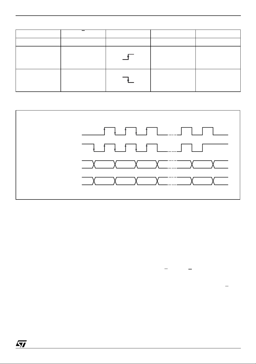
Table 2. Function Table
Mode E SCL SDI SDO
Disable Reset H Input Disabled Input Disabled High Z
M41T94
WRITE L Data Bit latch High Z
READ L X
Note: 1. SD O remains at High Z until ei ght bits of data are ready to be shifted out duri ng a READ.
AI04630
AI04631
Figure 8. Dat a and Clock Timi ng
CPOL
CPHA
0
1
0
1
C
C
SDI
SDO
MSB
MSB
Next data bit shift
LSB
LSB
AI04632
(1)
Signal Description
Serial Data Output (SDO). The output pin is
used to transfer data serially out of the Memory.
Data is shifted out on the fallin g edge of the serial
clock.
Serial Data Input (SDI). The input pin is used to
transfer data serially into t he device. Instructions,
addresses, and the data to be written, are each received this way. Input is latched on the rising edge
of the serial clock.
Serial Clock (SCL). The serial c lock provides the
timing for the serial interface (as shown in Figure
10, page 12 and Figure 11, page 12). The W/R Bit,
addresses, or data are latched, from the input pin,
on the rising edge of the clock input. The output
data on the SDO pin changes state after the falling
edge of the clock input.
The M41T94 can be d riven by a microcontroller
with its SPI periphe ral running in ei the r of the two
following modes:
(CPOL, CPHA) = ('0', '0') or
(CPOL, CPHA) = ('1', '1').
For these two modes, input data (SDI) is latched in
by the low-to-high transition of clock SCL, and output data (SDO) is shifted out on t he high-to-low
transition of SCL (see Table 2, page 7 and Figure
8, page 7).
Chip Enable (E
). When E is high, the memory
device is deselected, and the SDO output pin is
held in its high impedance state.
After power-on, a high-to-low transition on E
is re-
quired prior to the start of any operation.
7/31
M41T94
MAXIMUM RATI N G
Stressing the device ab ove the rating listed in t he
“Absolute Maximum Ratings” table may cause
permanent damage to the device. These are
stress ratings only and operation of the dev ice at
these or any other conditions above those indicated in the Operating sections of this specification is
Table 3. Absolute Maximum Ratings
Symbol Parameter Value Unit
T
STG
Storage Temperature (VCC Off, Oscillator Off)
not implied. Exposure to Absol ute Maxim um Ra ting conditions for extended periods may affect device reliability. Refer also to the
STMicroelectronics SURE Program and other relevant quality documents.
SNAPHAT –40 to 85 °C
SOIC –55 to 125 °C
V
CC
T
SLD
V
IO
I
O
P
D
Note: 1. Ref l ow at peak t em perature of 215°C t o 225°C for < 60 seconds (total thermal budget not to exceed 180° C for betw een 90 to 120
CAUTION: Negative undershoots below –0.3V are not allowed on any pin while in the Battery Back-up mode.
CAUTION: Do NOT wave solder SOIC to avoid damaging S NA PHAT sockets.
Supply Voltage –0.3 to 7 V
(1)
Lead Solder Temperature for 10 seconds 260 °C
Input or Output Voltage
Output Current 20 mA
Power Dissipation 1 W
secon ds).
–0.3 to V
CC
+0.3
V
8/31
DC AND AC PARAMETERS
This section summarizes the operat ing and measurement conditions, as well as the DC and AC
characteristics of the device. The parameters in
the following DC and AC Characteristic tables are
ment Conditions listed in the rel evant tables. Designers should check that the operating conditions
in their projects match the measurement conditions when using the quoted parameters.
derived from tests performed under the M easure-
Table 4. DC and AC Measurement Conditions
Parameter M41T94
V
Supply Voltage
CC
2.7 to 5.5V
Ambient Operating Temperature –40 to 85°C
Load Capacitance (C
)
L
100pF
Input Rise and Fall Times ≤ 50ns
Input Pulse Voltages
Input and Output Timing Ref. Voltages
Note: Output Hi -Z is defined as the point where dat a i s no longer dri ven.
0.2 to 0.8V
0.3 to 0.7V
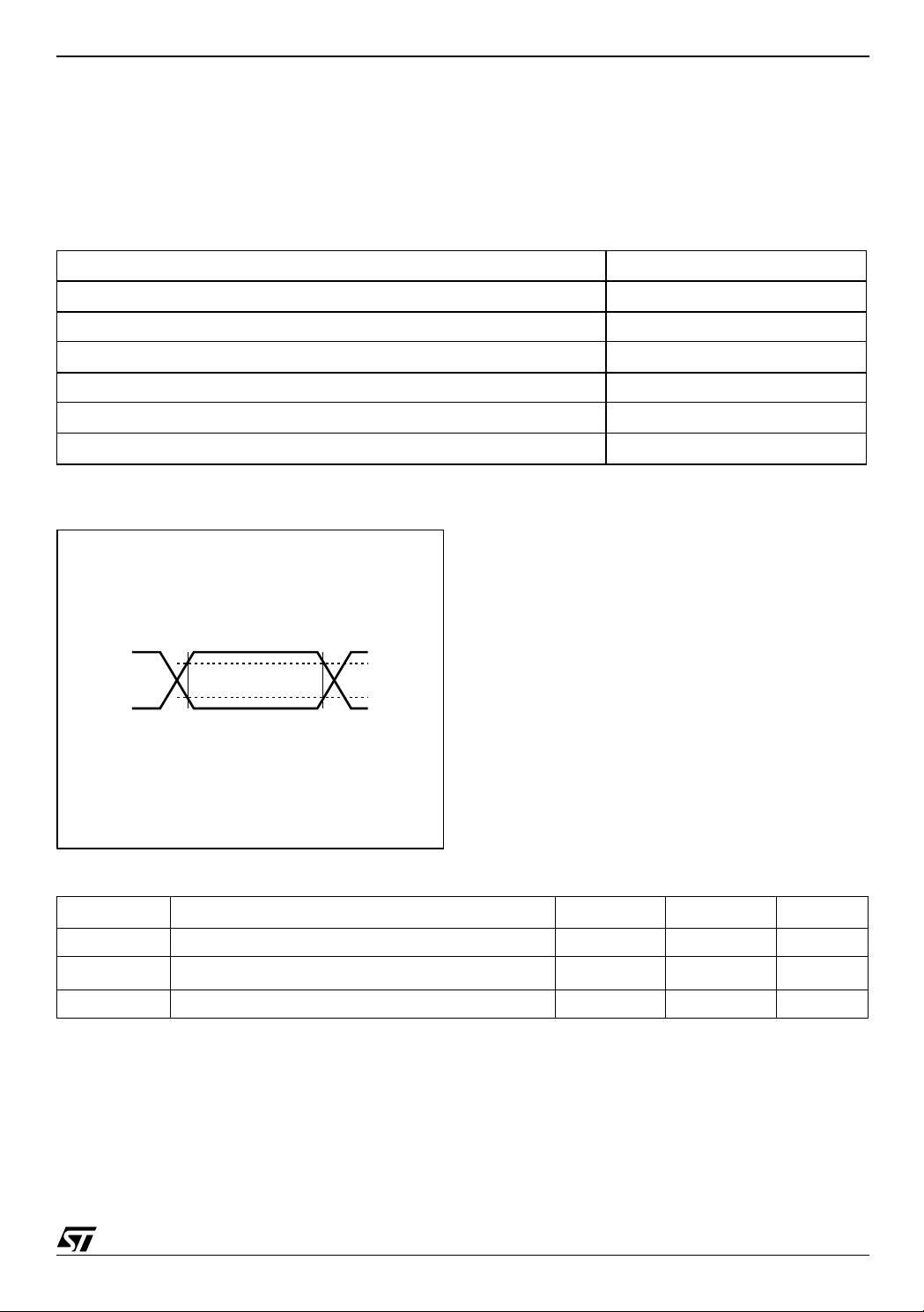
Figure 9. AC Testing Input/Output Waveforms
M41T94
CC
CC
0.8V
0.2V
CC
CC
0.7V
0.3V
AI02568
CC
CC
Table 5. Capacitance
Symbol
C
IN
C
OUT
t
LP
Note: 1. Effective c apacitance measure d wi th power supply at 5V ; s am pl ed only, n ot 100% teste d.
2. At 25°C, f = 1MHz.
3. Outputs are deselect ed.
Input Capacitance 7 pF
(3)
Output Capacitance 10 pF
Low-pass filter input time constant (SDA and SCL) 50 ns
Parameter
(1,2)
Min Max Unit
9/31
M41T94
Table 6. DC Characteristics
= 3V
CC
≤ V
≤ V
(1)
– 0.3V
CC
CC
Min Typ Max Unit
400 500 nA
0.7V
CC
2.4 V
4.20 4.40 4.50
2.55 2.60 2.70
Symb. Parameter
Battery Current OSC ON
I
BAT
Battery Current OSC OFF 50 nA
I
I
I
I
LO
V
V
V
Supply Current f = 2 MHz 2 mA
CC1
Supply Current (Standby)
CC2
(2)
Input Leakage Current
LI
(3)
Output Leakage Current
V
Input High Voltage
IH
V
Input Low Voltage –0.3
IL
Battery Voltage 2.5
BAT
OH
Output High Voltage
Output Low Voltage
OL
(4)
(4)
Output Low Voltage (Open Drain)
(5)
Test Condition
= 25°C, VCC = 0V,
T
A
V
BAT
SCL, SDI = V
0V ≤ V
IN
0V ≤ V
OUT
IOH = –1.0mA
IOL = 3.0mA
IOL = 10mA
Power Fail Deselect (THS = VCC)
V
PFD
Power Fail Deselect (THS = V
V
Note: 1. Va lid for Ambi ent Operat in g T emperat ure: TA = –40 to 85°C ; VCC = 2.7 to 5. 5V (except where note d).
Battery Back-up Switchover 2.5 V
SO
2. RSTIN1
3. Outputs Dese l ected.
4. For SQW pi n (CMOS).
5. For IRQ
6. For rechargeable ba ck-up, V
and RSTI N2 internally pulled-up t o VCC through 100KΩ resistor. WDI internally pulled-down to VSS through 100KΩ resistor.
/FT/OUT, RST pins (Ope n Drai n): i f pu ll ed- up to supp ly oth e r tha n VCC, this su ppl y mu st be equ al to, or l es s t han 3. 0V when
= 0V (durin g battery back-up mode).
V
CC
(max) may be considered VCC.
BAT
SS
)
1.4 mA
±1 µA
±1 µA
VCC + 0.3
0.3V
CC
(6)
3.5
0.4
0.4
V
V
V
V
V
Table 7. Crystal Electrical Characteristics (Externally Supplied)
Symbol
f
0
R
S
C
L
Note: 1. Load capacitors are integrated within the M41T94. Circuit board layout considerations for the 32.768 kHz crystal of minimum trace
lengths an d i solation from RF genera ting signals should be taken into acco unt. These characteristics are e xt ernally sup pl i ed.
2. STMicroelectronics recommends the KDS DT-38: 1TA/1TC252E127, Tuning Fork Type (thru-hole) or the DMX-26S:
1TJS125 F H2A212, (SM D) quartz crystal for ind u s trial temperature operations. KDS can be contacted at k ouhou@kds j .co.jp or ht tp://www.kdsj.co.jp for further information on this crystal type.
Resonant Frequency 32.768 kHz
Series Resistance 50 kΩ
Load Capacitance 12.5 pF
Parameter
10/31
(1,2)
Typ Min Max Unit
 Loading...