

SERIAL ACCESS RTC WITH ALARMS
FEATURES SUMMARY
■ 2.0 TO 5.5V CLOCK OPERATING VOLT A GE
■ COUNTERS FOR TENTHS/HUNDREDTHS
OF SECONDS, SECONDS, MINUTES,
HOURS, DAY, DATE , MONTH, YEAR, and
CENTURY
■ AUTOMATIC SWITCH-OVER and DESELECT
CIRCUITRY
■ SERIAL INTERFAC E SU PPO R TS I
(400KHz PROTOCOL)
■ PROGRAMMABLE ALAR M and INTERRUPT
FUNCTION (valid even during Battery Back-up
Mode)
■ WATCHDOG T IM E R
■ LOW OPERATING CURRENT OF 400µA
■ BATTERY BACK-UP NOT RECOMMENDED
FOR 3.0V APPLICAT IO N S (C APAC ITOR
BACK-UP ONLY)
■ BATTERY OR SUPER-CAP BACK-UP
■ OPERATING TEMPERATURE OF –40 TO
85°C
■ ULTRA-LOW BATTERY SU PPL Y C URRENT
OF 1µA
■ PACKAGE OPTI ONS INCLUDE A 28-LEAD o r
18-LEAD EMBE DDE D CRYSTAL SOIC
2
C BUS
M41T81
Figure 1. 8-pi n S OI C Package
8
1
SO8 (M)
Figure 2. 28-pin (300mil) SOIC Package*
EMBEDDED Crystal
SOX28 (MX)
Figure 3. 18-pin (300mil) SOIC Package*
EMBEDDED Crystal
18
1
SOX18 (MY)
Rev. 2.0
1/28September 2003

M41T81
TABLE OF CONTENTS
SUMMARY DESCRIPTION. . . . . . . . . . . . . . . . . . . . . . . . . . . . . . . . . . . . . . . . . . . . . . . . . . . . . . . . . . . 4
Figure 4. Logic Diagram . . . . . . . . . . . . . . . . . . . . . . . . . . . . . . . . . . . . . . . . . . . . . . . . . . . . . . . . . . 4
Table 1. Signal Names . . . . . . . . . . . . . . . . . . . . . . . . . . . . . . . . . . . . . . . . . . . . . . . . . . . . . . . . . . . 4
Figure 5. 8-pin SOIC (M) Connections . . . . . . . . . . . . . . . . . . . . . . . . . . . . . . . . . . . . . . . . . . . . . . . 5
Figure 7. 28-pin, 300mil SOIC (MX) Connections . . . . . . . . . . . . . . . . . . . . . . . . . . . . . . . . . . . . . . . 5
Figure 6. 18-pin, 300mil SOIC (MY) Connections . . . . . . . . . . . . . . . . . . . . . . . . . . . . . . . . . . . . . . . 5
Figure 8. Block Diagram . . . . . . . . . . . . . . . . . . . . . . . . . . . . . . . . . . . . . . . . . . . . . . . . . . . . . . . . . . 5
MAXIMUM RATING. . . . . . . . . . . . . . . . . . . . . . . . . . . . . . . . . . . . . . . . . . . . . . . . . . . . . . . . . . . . . . . . . 6
Table 2. Absolute Maximum Ratings. . . . . . . . . . . . . . . . . . . . . . . . . . . . . . . . . . . . . . . . . . . . . . . . . 6
DC AND AC PARAMETERS. . . . . . . . . . . . . . . . . . . . . . . . . . . . . . . . . . . . . . . . . . . . . . . . . . . . . . . . . . 7
Table 3. Operating and AC Measurement Conditions. . . . . . . . . . . . . . . . . . . . . . . . . . . . . . . . . . . . 7
Figure 9. AC Measurement I/O Waveform . . . . . . . . . . . . . . . . . . . . . . . . . . . . . . . . . . . . . . . . . . . . 7
Table 4. Capacitance. . . . . . . . . . . . . . . . . . . . . . . . . . . . . . . . . . . . . . . . . . . . . . . . . . . . . . . . . . . . . 7
Table 5. DC Characteristics. . . . . . . . . . . . . . . . . . . . . . . . . . . . . . . . . . . . . . . . . . . . . . . . . . . . . . . . 8
Table 6. Crystal Electrical Characteristics. . . . . . . . . . . . . . . . . . . . . . . . . . . . . . . . . . . . . . . . . . . . . 8
OPERATION . . . . . . . . . . . . . . . . . . . . . . . . . . . . . . . . . . . . . . . . . . . . . . . . . . . . . . . . . . . . . . . . . . . . . . 9
2-Wire Bus Characteristics. . . . . . . . . . . . . . . . . . . . . . . . . . . . . . . . . . . . . . . . . . . . . . . . . . . . . . . 9
Figure 10. Serial Bus Data Transfer Sequence. . . . . . . . . . . . . . . . . . . . . . . . . . . . . . . . . . . . . . . . 10
Figure 11. Acknowledgement Sequence. . . . . . . . . . . . . . . . . . . . . . . . . . . . . . . . . . . . . . . . . . . . . 10
Figure 12. Bus Timing Requirements Sequence. . . . . . . . . . . . . . . . . . . . . . . . . . . . . . . . . . . . . . . 11
Table 7. AC Characteristics . . . . . . . . . . . . . . . . . . . . . . . . . . . . . . . . . . . . . . . . . . . . . . . . . . . . . . . 1 1
READ Mode . . . . . . . . . . . . . . . . . . . . . . . . . . . . . . . . . . . . . . . . . . . . . . . . . . . . . . . . . . . . . . . . . . 12
Figure 13. Slave Address Location . . . . . . . . . . . . . . . . . . . . . . . . . . . . . . . . . . . . . . . . . . . . . . . . . 12
Figure 14. READ Mode Sequence . . . . . . . . . . . . . . . . . . . . . . . . . . . . . . . . . . . . . . . . . . . . . . . . . 12
Figure 15. Alternative READ Mode Sequence . . . . . . . . . . . . . . . . . . . . . . . . . . . . . . . . . . . . . . . . 13
WRITE Mode. . . . . . . . . . . . . . . . . . . . . . . . . . . . . . . . . . . . . . . . . . . . . . . . . . . . . . . . . . . . . . . . . . 13
Figure 16. WRITE Mode Sequence . . . . . . . . . . . . . . . . . . . . . . . . . . . . . . . . . . . . . . . . . . . . . . . . . 13
Data Retention Mode. . . . . . . . . . . . . . . . . . . . . . . . . . . . . . . . . . . . . . . . . . . . . . . . . . . . . . . . . . . 14
Figure 17. Power Down/Up Mode AC Waveforms . . . . . . . . . . . . . . . . . . . . . . . . . . . . . . . . . . . . . 14
Table 8. Power Down/Up AC Characteristics . . . . . . . . . . . . . . . . . . . . . . . . . . . . . . . . . . . . . . . . . 14
Table 9. Power Down/Up Trip Points DC Characteristics . . . . . . . . . . . . . . . . . . . . . . . . . . . . . . . . 14
CLOCK OPERATION . . . . . . . . . . . . . . . . . . . . . . . . . . . . . . . . . . . . . . . . . . . . . . . . . . . . . . . . . . . . . . 15
TIMEKEEPER® Registers. . . . . . . . . . . . . . . . . . . . . . . . . . . . . . . . . . . . . . . . . . . . . . . . . . . . . . . 1 5
Table 10. TIMEKEEPER® Register Map . . . . . . . . . . . . . . . . . . . . . . . . . . . . . . . . . . . . . . . . . . . .16
Calibrating the Clock. . . . . . . . . . . . . . . . . . . . . . . . . . . . . . . . . . . . . . . . . . . . . . . . . . . . . . . . . . . 17
Setting Alarm Clock Registers. . . . . . . . . . . . . . . . . . . . . . . . . . . . . . . . . . . . . . . . . . . . . . . . . . . 1 8
Figure 18. Alarm Interrupt Reset Waveform . . . . . . . . . . . . . . . . . . . . . . . . . . . . . . . . . . . . . . . . . . 18
2/28

M41T81
Figure 19. Back-up Mode Alarm Waveform . . . . . . . . . . . . . . . . . . . . . . . . . . . . . . . . . . . . . . . . . . 18
Table 11. Alarm Repeat Modes. . . . . . . . . . . . . . . . . . . . . . . . . . . . . . . . . . . . . . . . . . . . . . . . . . . . 19
Watchdog Timer . . . . . . . . . . . . . . . . . . . . . . . . . . . . . . . . . . . . . . . . . . . . . . . . . . . . . . . . . . . . . . 19
Square Wave Outp ut . . . . . . . . . . . . . . . . . . . . . . . . . . . . . . . . . . . . . . . . . . . . . . . . . . . . . . . . . . . 20
Table 12. Square Wave Output Frequency . . . . . . . . . . . . . . . . . . . . . . . . . . . . . . . . . . . . . . . . . . . 20
Century Bit. . . . . . . . . . . . . . . . . . . . . . . . . . . . . . . . . . . . . . . . . . . . . . . . . . . . . . . . . . . . . . . . . . . 21
Output Driver Pin . . . . . . . . . . . . . . . . . . . . . . . . . . . . . . . . . . . . . . . . . . . . . . . . . . . . . . . . . . . . . . 21
Preferred Initial Power-on Default . . . . . . . . . . . . . . . . . . . . . . . . . . . . . . . . . . . . . . . . . . . . . . . . 21
Table 13. Preferred Default Values . . . . . . . . . . . . . . . . . . . . . . . . . . . . . . . . . . . . . . . . . . . . . . . . . 21
Figure 20. Crystal Accuracy Across Temperature . . . . . . . . . . . . . . . . . . . . . . . . . . . . . . . . . . . . . . 22
Figure 21. Clock Calibration . . . . . . . . . . . . . . . . . . . . . . . . . . . . . . . . . . . . . . . . . . . . . . . . . . . . . . 22
PACKAGE MECHANICAL INFORMATION . . . . . . . . . . . . . . . . . . . . . . . . . . . . . . . . . . . . . . . . . . . . . 23
PART NUMBERING . . . . . . . . . . . . . . . . . . . . . . . . . . . . . . . . . . . . . . . . . . . . . . . . . . . . . . . . . . . . . . . 26
REVISION HISTORY. . . . . . . . . . . . . . . . . . . . . . . . . . . . . . . . . . . . . . . . . . . . . . . . . . . . . . . . . . . . . . . 27
3/28
M41T81
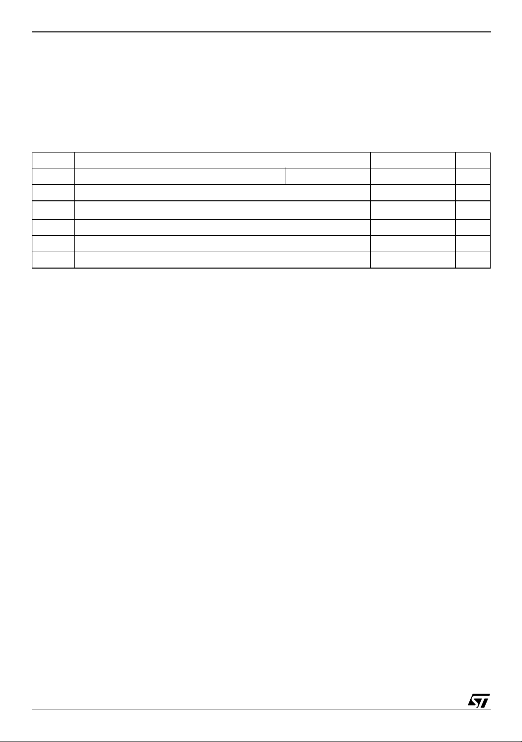
SUMMARY DESCRIPTION
The M41T81 Serial Access TIMEKEEPER
SRAM is a low power Serial RTC with a b uilt-in
32.768 KHz oscillator (external crystal controlled).
Eight bytes of the SRA M (see Table 10, page 16)
are used for the c lock/calendar function and are
configured in binary coded decimal (BCD) form at.
An additional 12 bytes of SRAM provide status/
control of Alarm, Watchdog and Square Wave
functions. Addresses and data are transferred serially via a two line, bi-directional I
2
C in ter fac e. The
built-in address register is incremented automatically after each WRITE or READ data byte.
The M41T81 has a built-in power sense circuit
which detects power failures and automatically
switches to the battery supply when a power f ailure occurs. The energy needed to sustain the
SRAM and clock operations can be supplied by a
Figure 4. Logic Diagram
V
V
BAT
CC
(1)
XI
(1)
XO
SCL
SDA
M41T81
IRQ/FT/OUT/SQW
®
small lithium button supply when a po wer failure
occurs. Functions avai lable to the user include a
non-volatile, time-of-day clock/calendar, Alarm interrupts, Watchdog Timer and programmable
Square Wave output. The eight clock address locations contain the century, year, month, date,
day, hour, minute, second and tenths/hundredths
of a second in 24 hour BCD format. Corrections for
28, 29 (leap year - valid until year 2100), 30 and 31
day months are made automatically.
The M41T81 is supplied in either an 8-pin SOIC or
an 18-pin (MY) or 28-pin (MX), 300mil SOIC package which includes an embedded 32kHz crystal.
The 8-pin and 28-pin, embedd ed c rystal SOI C requires only a user-supplied battery to provide nonvolatile operation.
Table 1. Signal Names
(1)
XI
(1)
XO
IRQ
/OUT/
FT/SQW
SDA Serial Data Input/Output
SCL Serial Clock Input
V
BAT
Oscillator Input
Oscillator Output
Interrupt / Output Driver / Frequency
Test / Square Wave (Open Drain)
Battery Supply Voltage
V
SS
Note: 1. For SO8 package only.
4/28
AI04613
V
CC
V
SS
Note: 1. For SO8 package only.
Supply Voltage
Ground
M41T81
Figure 5. 8-pin SOIC (M) Connections
1
XI
2
XO
V
BAT
V
SS
M41T81
3
45
8
V
CC
7
IRQ/FT/OUT/SQW
6
SCL
SDA
AI04769
Figure 6. 18-pin, 300mil SOIC (MY) Connections
1
NC
2
NC
3
NC
4
NC
5
NC
6
NC
7
NC
V
BAT
V
SS
8
9
M41T81
18
NC
17
NC
16
NC
15
V
14
NC
13
IRQ/FT/OUT/SQW
12
NC
11
SCL
10
SDA
CC
AI07830
Figure 8. Block Diagram
Figure 7. 28-pin, 300mil SOIC (MX) Connections
1
NC
2
NC
3
NC
4
NC
5
NC
6
NC
7
NC
NC
NC
NC
NC
8
9
10
11
M41T81
12
V
V
Note: 1. No Connect (NC) pin for 28-pin SOIC, but should be con-
13
BAT
14
SS
sidered t o have indicat ed function i n anticipation of replacement with 18-pin S O I C.
28
V
27
NC
26
IRQ/FT/OUT/SQW
25
NC
V
24
23
NC
22
SCL
21
NC
20
V
19
NC
18
IRQ/FT/OUT/SQW
17
SDANC
16
SCL
15
SDA
CC
CC
SS
(1)
(1)
(1)
(1)
AI07805
CRYSTAL
SDA
SCL
V
CC
V
BAT
Note 1. Open drain output
Note 2. VSO = V
– 0.5V (typ)
BAT
V
SO
OSCILLATOR
INTERFACE
(2)
COMPARE
32KHz
I2C
PROTECT
WRITE
REAL TIME CLOCK
CALENDAR
RTC W/ALARM
& CALIBRATION
WATCHDOG
SQUARE WAVE
INTERNAL
AFE
WDF
SQWE
POWER
IRQ/FT/OUT/SQW
AI04616
(1)
5/28
M41T81
MAXIMUM RATI N G
Stressing the device ab ove the rating listed in t he
“Absolute Maximum Ratings” table may cause
permanent damage to the device. These are
stress ratings only and operation of the dev ice at
these or any other conditions above those indicated in the Operating sections of this specification is
Table 2. Absolute Maximum Ratings
Sym Parameter Value Unit
T
STG
V
T
SLD
V
P
Note: 1. Reflow at peak temp erature of 2 15°C to 225°C for < 60 s econds (to tal therma l budget not to exceed 180° C for betw een 90 to 12 0
Storage Temperature (VCC Off, Oscillator Off)
Supply Voltage
CC
(1)
Lead Solder Temperature for 10 Seconds 260 °C
Input or Output Voltages –0.3 to Vcc+0.3 V
IO
I
Output Current 20 mA
O
Power Dissipation 1 W
D
secon ds).
CAUTION: Negative under shoots below –0.3 volts ar e not allowed on any pin while i n the Batter y B ack-Up Mode
not implied. Exposure to Absol ute Maxim um Ra ting conditions for extended periods may affect device reliability. Refer also to the
STMicroelectronics SURE Program and other relevant quality documents.
SOIC –55 to 125
–0.3 to 7
°C
V
6/28
DC AND AC PARAMETERS
This section summarizes the operat ing and measurement conditions, as well as the DC and AC
characteristics of the device. The parameters in
the following DC and AC Characteristic tables are
derived from tests performed under the M easure-
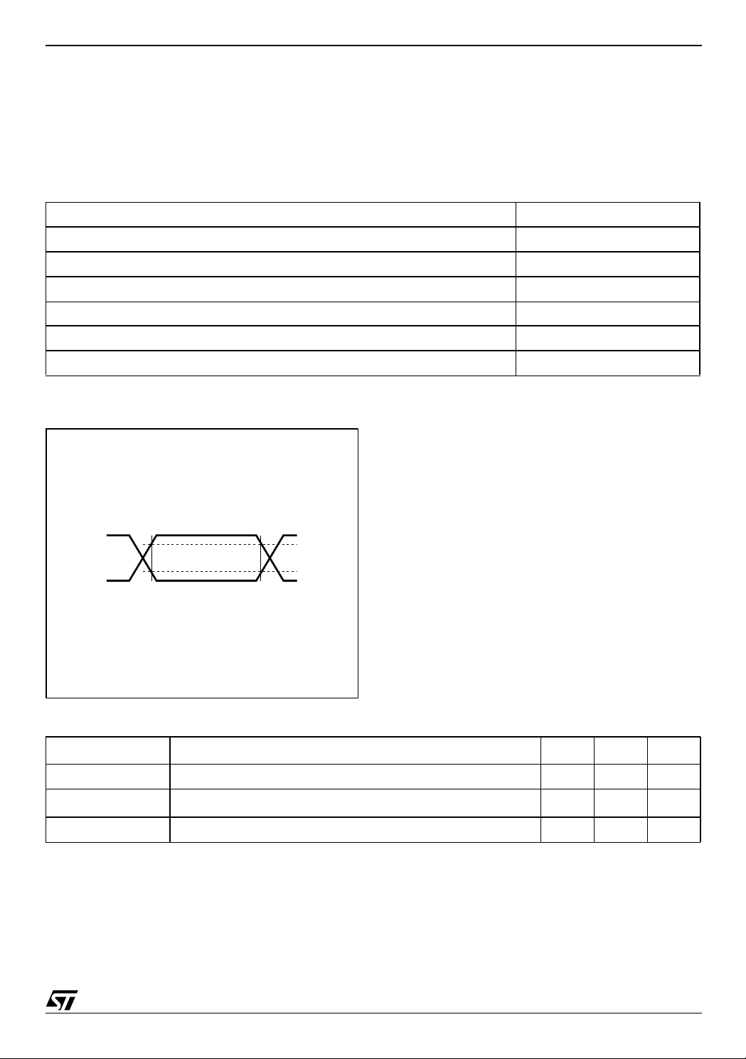
Table 3. Operating and AC Measurement Conditions
Parameter M41T81
M41T81
ment Conditions listed in the rel evant tables. Designers should check that the operating conditions
in their projects match the measurement conditions when using the quoted parameters.
Supply Voltage (V
Ambient Operating Temperature (T
Load Capacitance (C
CC
)
)
A
)
L
2.0 to 5.5V
–40 to 85°C
100pF
Input Rise and Fall Times ≤ 50ns
Input Pulse Voltages
Input and Output Timing Ref. Voltages
Note: Out put Hi-Z is def i ned as the poi nt where dat a i s no longer dri ven.
0.2VCC to 0.8 V
0.3V
to 0.7 V
CC
Figure 9. AC Measurement I/O Waveform
0.8V
0.2V
CC
CC
0.7V
0.3V
AI02568
CC
CC
CC
CC
Table 4. Capacitance
Symbol
C
IN
(3)
C
OUT
t
LP
Note: 1. Effective capacitance measured with power supply at 5V; sam p l ed only, not 100% tested.
2. At 25°C, f = 1MHz.
3. Outputs deselect ed.
Input Capacitance 7 pF
Output Capacitance 10 pF
Low-pass filter input time constant (SDA and SCL) 50 ns
Parameter
(1,2)
Min Max Unit
7/28
M41T81
Table 5. DC Characteristics
IN
≤ V
≤ V
CC
(1)
CC
CC
– 0.3V
= 3V
BAT
Min Typ Max Unit
0.7V
CC
(3)
2.5
0.6 1 µA
Sym Parameter
I
Input Leakage Current
LI
I
Output Leakage Current
LO
I
I
Supply Current Switch Freq = 400kHz 400 µA
CC1
Supply Current (standby)
CC2
V
Input Low Voltage –0.3
IL
V
Input High Voltage
IH
Output Low Voltage
V
OL
Output Low Voltage (Open Drain)
(2)
V
BAT
I
Note: 1. Valid for Ambient Operating T em perature: TA = –40 to 85°C ; VCC = 2.0 to 5. 5V (except wh ere noted ) .
Battery Supply Voltage
Battery Supply Current
BAT
2. STMic roelectronics recommends the RAYOVAC BR 1225 or BR16 32 (or equiva l ent) as the battery supply.
3. After s wi tchover (V
4. For re chargeabl e back-up, V
5. For IRQ
/FT/OUT/SQW pin (Open Drain)
SO
), V
(min) can be 2.0V for crystal with RS = 40KΩ.
BAT
(max) may be considered VCC.
BAT
(5)
Test Condition
0V ≤ V
0V ≤ V
OUT
SCL,SDA = V
I
= 3.0mA 0.4
OL
IOL = 10mA
T
= 25°C, VCC = 0V
A
Oscillator ON, V
3
±1 µA
±1 µA
100 µA
0.3V
CC
VCC + 0.3
0.4 V
(4)
3.5
V
V
V
V
Table 6. Crystal Electrical Characteristics
Sym
f
O
R
S
C
L
Note: 1. External ly supp lied if usin g th e SO8 pa ckag e. S TMic roe lectr onic s re com mend s th e KD S D T-38 : 1T A/1T C252 E127 , Tuni ng F ork
2. Load capacitors are in te grated within the M41T81. Circuit board layout considerations for the 32.768 kHz cryst al of m i ni m um trace
Resonant Frequency 32.768 kHz
Series Resistance
Load Capacitance 12.5 pF
Type (thru-hole) or the DMX-26S: 1TJS125FH2A212, (SMD) quartz crystal for industrial temperature operations. KDS can be contacted at kouhou@kds j .c o. j p or http:// www.kdsj.c o.jp for further inform ation on this cr ystal type.
lengths an d i solation from RF genera ting signals should be taken into acco unt.
Parameter
(1,2,3)
Min Typ Max Units
60
kΩ
8/28

OPERATION
The M41T81 clock operates as a slave device on
the serial bus. Access is obtained by implementing
a start condition followed by the correct slave address (D0h). The 20 bytes contained in the device
can then be accessed sequentially in the following
order:
1. Tenths/Hundredths of a Second Register
2. Seconds Register
3. Minutes Register
4. Century/Hours Register
5. Day Register
6. Date Register
7. Month Register
8. Year Register
9. Control Register
10. Watchdog Register
11 - 16. Alarm Registers
17 - 19. Reserved
20. Square Wave Register
The M41T81 clock continually monitors V
out-of-tolerance condition. Should V
V
, the device terminates an ac ces s in progress
SO
CC
for an
CC
fall be low
and resets the device add ress counter. Inputs to
the device will not be recognized at this time to
prevent erroneous data from being written to the
device fro m a an ou t-o f-tolerance syste m. The device also automatically switches over to the battery
and powers down into an ultra low current mode of
operation to conserve battery life. As system power returns and V
rises above VSO, the battery is
CC
disconnected, and the power supply is switched to
external V
CC
.
For more information on Battery Storage Life refer
to Application Note AN1012.
2-Wire Bus Characteristics
The bus is intended for communication between
different ICs. It consists of two lines: a bi-directional data signal (SDA) and a clock signal (SCL).
Both the SDA and SCL lines must be connected to
a positive supply voltage via a pull-up resistor.
The following protocol has been defined:
– Data transfer may be initiated only when the bus
is not busy.
– During data trans fer, the dat a line mus t remain
stable whenever the clock line is High.
M41T81
– Changes in the data line, while the clock line is
High, will be interpreted as control signals.
Accordingly, the following bus conditions have
been defined:
Bus not busy. Both data and clock lines remain
High.
Start data transfer. A c hange in the st ate of the
data line, from high to Low, while the clock is High,
defines the START condition.
Stop data transfer. A change in the state of the
data line, from Low to High, while the clock is High,
defines the STOP condition.
Data Valid. The state of the data line represents
valid data when after a start condition, the data line
is stable for the duration of the high period of the
clock signal. The data on the line may be changed
during the Low period of the clock signal. There is
one clock pulse per bit of data.
Each data transfer is initiated with a start condition
and terminated with a stop condition. The number
of data bytes transferred between the start and
stop conditions is not limited. The information is
transmitted byte-wide and each receiver acknowledges with a ninth bit.
By definition a device that gives out a message is
called “transmitter,” the receiving device that gets
the message is called “receiver.” The device that
controls the message is called “master.” The devices that are controlled by the master are cal led
“slaves.”
Acknowledge. Each byte of eight bits is followed
by one Acknowledge Bit. This Acknowledge Bit is
a low level put on the bus by the receiver whereas
the master generates an extra acknowledge related clock pulse. A slave receiver which is addressed is obliged to generate an acknowledge
after the reception of each byte that has been
clocked out of the slave transmitter.
The device that acknowledges has to pull down
the SDA line during the acknowledge clock pulse
in such a way that the SDA line is a stable Low during the High period of the acknowledge related
clock pulse. Of course, setup and hold times must
be taken into account. A master receiver must signal an end of data to the slave transm itter by not
generating an acknowledge on t he last byte that
has been clocked out of the slave. In this case the
transmitter must leave the data line High to enable
the master to generate the STOP condition.
9/28

M41T81
Figure 10. Serial Bus Data Transfer Sequence
DATA LINE
STABLE
DATA VALID
CLOCK
DATA
START
CONDITION
Figure 11. Acknowledgement Sequence
START
SCL FROM
MASTER
DATA OUTPUT
BY TRANSMITTER
DATA OUTPUT
BY RECEIVER
12 89
MSB LSB
CHANGE OF
DATA ALLOWED
STOP
CONDITION
AI00587
CLOCK PULSE FOR
ACKNOWLEDGEMENT
AI00601
10/28

Figure 12. Bus Timing Requirements Sequence
SDA
M41T81
tHD:STA
SCL
tHD:STAtBUF
tR
SP
tHIGH
tLOW
tF
tSU:DAT
tHD:DAT
SR
Table 7. AC Characteristics
Sym
f
SCL
t
LOW
t
HIGH
t
R
t
F
t
HD:STA
t
SU:STA
t
SU:DAT
t
HD:DAT
t
SU:STO
t
BUF
Note: 1. Valid for Ambient Operating T em perature: TA = –40 to 85°C ; VCC = 2.0 to 5. 5V (except wh ere noted ) .
2. Tran smi tter must in ternally p rovide a hold t i m e to b ridge the undef i ned region (300ns max ) of the fallin g edge of SCL.
SCL Clock Frequency 0 400 kHz
Clock Low Period 1.3 µs
Clock High Period 600 ns
SDA and SCL Rise Time 300 ns
SDA and SCL Fall Time 300 ns
START Condition Hold Time
(after this period the first clock pulse is generated)
START Condition Setup Time
(only relevant for a repeated start condition)
(2)
Data Setup Time 100 ns
Data Hold Time 0 µs
STOP Condition Setup Time 600 ns
Time the bus must be free before a new
transmission can start
Parameter
(1)
Min Typ Max Units
600 ns
600 ns
1.3 µs
tSU:STOtSU:STA
P
AI00589
11/28

M41T81
READ Mode
In this mode the master reads the M41T81 slave
after setting the slave address (see Figure 14,
page 12). Following the WRITE Mode Control Bit
=0) and the Acknowledge Bit, the word ad-
(R/W
dress 'An' is written to the on-chip address pointer.
Next the START condition and slave address are
repeated followed by the RE AD Mode Control Bit
(R/W
=1). At this point the master transmitter becomes the master receiver. The data byte which
was addressed will be transmi tted and the master
receiver will send an Acknowledge Bit to the slave
transmitter. The address pointer is only incremented on reception of an Acknowledge Clock. The
M41T81 s lave tr ansmitt er will now place the data
byte at address An+1 on the bus, the master receiver reads and acknowledges the n ew byte and
the address pointer is incremented to “An+2.”
Figure 13. Slave Address Location
This cycle of reading con secutive addresses will
continue until the mast er receiver sends a STOP
condition to the slave transmitter.
The system-to-user transfer of clock data will be
halted whenever the address being read is a clock
address (00h to 07h). The update will resume due
to a Stop Condition or when the pointer increments
to any non-clock address (08h-13h).
Note: This is true both in READ Mode and WRITE
Mode.
An alternate READ Mode may also be implemented whereby the master reads the M41T81 slave
without first writing to the (volatile) a ddress pointer. The first address that is read is the last one
stored in the pointer (see Figure 15, page 13).
R/W
START A
Figure 14. READ Mode Sequence
BUS ACTIVITY:
MASTER
SDA LINE
BUS ACTIVITY:
START
S
ADDRESS
R/W
SLAVE
WORD
ADDRESS (An)
ACK
STOP
SLAVE ADDRESS
MSB
0100011
START
S
ACK
SLAVE
ADDRESS
LSB
AI00602
R/W
DATA n DATA n+1
ACK
ACK
ACK
12/28
DATA n+X
P
AI00899
NO ACK

Figure 15. Alternative READ Mode Sequence
M41T81
BUS ACTIVITY:
MASTER
BUS ACTIVITY:
START
S
SLAVE
ADDRESS
R/W
DATA n DATA n+1 DATA n+X
ACK
WRITE Mode
In this mode the master transmitter transmits to
the M41T81 slave receiver. Bus protocol is shown
in Figure 16, page 13. Following the S TART condition and slave address, a logic '0' (R/W
=0) is
placed on the bus and indicates to the addressed
device th at w o rd address “ An ” w ill follow an d is to
be written to the on-chip address pointer. The data
word to be written to the memory is strobed in next
Figure 16. WRITE Mode S equence
BUS ACTIVITY:
MASTER
START
R/W
STOP
PSDA LINE
ACK
ACK
ACK
NO ACK
AI00895
and the internal address pointer is incremented to
the next address location on the reception of an
acknowledge clock. The M41T81 slave receiver
will send an acknowledge clock to the master
transmitter after it has received t he sla ve address
see Figure 13, page 12 and aga in after it has received the word address and each data byte.
STOP
BUS ACTIVITY:
S
ADDRESS
SLAVE
WORD
ADDRESS (An)
ACK
DATA n DATA n+1 DATA n+X
ACK
ACK
ACK
PSDA LINE
ACK
AI00591
13/28

M41T81
Data Retention Mode
With valid V
cessed as described above with REA D or WRI TE
Cycles. Should the supply voltage decay, the power input will be switched from the V
battery when V
Switchover Voltage (V
registers will be maintained by the attached battery supply. As V
Figure 17. Power Down/Up Mode AC Waveforms
Table 8. Power Down/Up AC Characteristics
Symbol
t
PD
t
REC
Note: 1. VCC fall time should not exc eed 5mV/µs .
2. Vali d fo r Ambient Op erating Temperature : T
applied, the M41T81 can be ac-
CC
pin to the
CC
V
CC
VSO
SDA
SCL
falls below the Battery Back-up
CC
CC
). At this time the clock
SO
continues to fall, the M41T81
tPD
Parameter
SCL and SDA at VIH before Power Down
SCL and SDA at VIH after Power Up
DON'T CARE
(1,2)
= –40 to 85°C ; VCC = 2.0 to 5. 5V (except wh ere noted ) .
A
will pass through the Register Bit Reset Voltage
) threshold, not only write protecting itself,
(V
RST
but also resetting certain Control Bits (see Table
13, page 21). On power-up, when V
nominal value, write protection continues for t
returns to a
CC
REC
For a further, more detailed review of lifetime calculations, please see Application Note AN1012.
tREC
AI00596
Min Typ Max Unit
0nS
10 µS
.
Table 9. Power Down/Up Trip Points DC Characteristics
Sym
V
Battery Back-up Switchover Voltage
SO
V
Note: 1. All voltages referenced to VSS.
Register Bit Reset Voltage 1.1 2.0 V
RST
2. Vali d fo r Ambient Op erating Temperature : T
Parameter
(1,2)
V
BAT
= –40 to 85°C ; VCC = 2.0 to 5. 5V (except wh ere noted ) .
A
Min
– 0.80 V
Typ Max Unit
– 0.50 V
BAT
BAT
– 0.30
V
14/28

CLOCK OPERATION
The 20-byte Register Map (see Table 10, page 16)
is used to both set the clock and to read t he date
and time from the clock, in a binary coded decimal
format. Tenths/Hundredths of S econds, Seconds,
Minutes, and Hours are contained within the f irst
four registers.
Note: A WRIT E to any c lock reg ister w ill resu lt in
the Tenths/Hundredths of Seconds bei ng reset to
“00,” and Tenths/Hundredths of Seconds cannot
be written to any value other than “00.”
Bits D6 and D7 of Clock Register 03h (Century/
Hours Register) contain the CENTURY ENABLE
Bit (CEB) and the CENTURY Bit (CB). Setting
CEB to a '1' will cause CB to toggle, either from '0'
to '1' or from '1' to '0' at the turn of the century (depending upon its initial state). If CEB is set to a '0,'
CB will not toggle. Bits D0 through D2 of Regi ster
04h contain the Day (day of week). Registers 05h,
06h, and 07h contain the Date (day of month),
Month and Years. The ninth clock register is the
Control Register (this is described in the Clock
Calibration section). Bit D7 of Register 01h contains the S TOP Bit (ST). Sett ing th is bit to a '1' wil l
cause the oscillator to stop. If the device is expected to spend a significant amount of time on the
shelf, the oscillator may be stopped to reduce current drain. When reset to a '0' the oscillator restarts
within one second.
The eight Clock Registers may be read one byte at
a time, or in a sequential block. T he Cont rol Register (Address location 08h) may be accessed independently. Provision has been made to assure
that a clock update does not occur while any of the
M41T81
eight clock addresses are being read. If a clock address is being read, an update of the clock registers will be halte d. This will pr event a trans ition of
data during the READ.
Note: When a power failure occurs, the HT Bit will
automatically be set to a '1.' This will prevent t he
clock from updating the TIMEKEEPER
and will allow the user to read the exact time of the
power-down event. Resetting the HT Bit to a '0' will
allow the clock to update the TIMEKEEPER registers with the current time.
®
TIMEKEEPER
Registers
The M41T81 offers 20 internal registers which
contain Clock, Alarm, Watchdog, Flag, Square
Wave and Control data. These registers are memory locations which contain external (user accessible) and internal copies of the data (usually
referred to as BiPORT
™
TIMEKEEPER cel ls). The
external copies are in dependent of internal f unctions except that they are updated p eriodically by
the simultaneous transfer of the incremented internal copy. The internal divider (or clock) chain will
be reset upon the completion of a WRITE to any
clock address.
The system-to-user transfer of clock data will be
halted whenever the address being read is a clock
address (00h to 07h). The update will resum e either due to a Stop Condition or when the pointer
increments to any non-clock address (08h-13h).
TIMEKEEPER and Alarm Registers store data in
BCD. Control, Watchdog and Square Wave Registers store data in Binary Format.
®
registers,
15/28

M41T81
Table 10. TIMEKEEPER® Register Map
Addr
D7 D6 D5 D4 D3 D2 D1 D0
00h 0.1 Seconds 0.01 Seconds Seconds 00-99
01h ST 10 Seconds Seconds Seconds 00-59
02h 0 10 Minutes Minutes Minutes 00-59
03h CEB CB 10 Hours Hours (24 Hour Format)
04h 0 0 0 0 0 Day of Week Day 01-7
05h 0 0 10 Date Date: Day of Month Date 01-31
06h 0 0 0 10M Month Month 01-12
07h 10 Years Year Year 00-99
08h OUT FT S Calibration Control
09h 0 BMB4 BMB3 BMB2 BMB1 BMB0 RB1 RB0 Watchdog
0Ah AFE SQWE ABE Al 10M Alarm Month Al Month 01-12
0Bh RPT4 RPT5 AI 10 Date Alarm Date Al Date 01-31
0Ch RPT3 HT AI 10 Hour Alarm Hour Al Hour 00-23
0Dh RPT2 Alarm 10 Minutes Alarm Minutes Al Min 00-59
0Eh RPT1 Alarm 10 Seconds Alarm Seconds Al Sec 00-59
0FhWDFAF000000 Flags
Function/Ran ge
BCD Format
Century/
Hours
0-1/00-23
10h00000000Reserved
11h00000000Reserved
12h00000000Reserved
13hRS3RS2RS1RS00000SQW
Keys : S = Sign Bit
FT = Frequency Test Bit
ST = Stop Bit
0 = Must be set to '0'
BMB0-BMB4 = Watchdog Multiplier Bits
CEB = Century Enable Bit
CB = Centur y B i t
OUT = Output level
ABE = Alarm in Battery Back-up Mode Enable Bit
AFE = Alarm Flag Enable Flag
RB0-RB 1 = Watchdog R esolution Bits
RPT1-RPT5 = Alarm Repeat Mode Bit s
WDF = Watchdog Flag (Read only)
AF = Alarm Flag (Read onl y)
SQWE = Square Wave Enable
RS0-RS 3 = S Q W Frequency
HT = Halt Up date Bit
16/28

Calib rating the Clock
The M41T81 is driven by a quartz controlled oscillator with a nominal frequency of 32,768 Hz. The
devices are tested not exceed –25 to +45 PPM
(parts per million) oscillator frequency error at
o
C, which equates to about +1.9 to –1.1 minutes
25
per month (see Figure 20, page 22). When the
Calibration circuit is properly employed, accuracy
improves to better than +1/–2 PPM at 25°C.
The oscillation rate of crystals changes with temperature. The M41T81 design employs periodic
counter correction. The calibration c ircuit adds or
subtracts counts from the o scillator divider circuit
at the divide by 256 stage, as shown in Figure 21,
page 22. The number o f times pulses which are
blanked (subtracted, n egative calibration) or split
(added, positive calibration) depends upon the
value loaded into the five Calibration Bits found in
the Control Register. Adding counts speeds the
clock up, subtracting counts slows the clock down.
The Calibration Bits occupy the five lower order
bits (D4-D0) in the Control Register 08h. These
bits can be set to represent any value between 0
and 31 in binary form. Bit D5 is a Sign Bit; '1' indicates positive calibration, '0' indicates negative
calibration. Calibration occurs within a 64 m inute
cycle. The first 62 m inutes i n t he c ycle m ay , onc e
per minute, have one second either shortened by
128 or lengthened by 256 oscillator cycles. If a binary '1' is loaded into the register, only the first 2
minutes in the 64 minute cycle will be modified; if
a binary 6 is loaded, t he first 12 will be affected,
and so on.
Therefore, each cal ibration step has the effect of
adding 512 or subtracting 256 oscillator cycles for
every 125,829,120 actual oscillator cycles, that is
+4.068 or –2.034 PPM of adjustm ent per calibration step in the cal ibration registe r. Ass um ing that
the oscillator is running at exactly 32,768 Hz, each
of the 31 increments in the Calibration byte would
represent +10.7 or –5.35 seconds per month
M41T81
which corresponds to a total range of +5.5 or –2.75
minutes per month.
Two methods are available for ascertaining how
much calibration a given M41T81 may require.
The first involves setting the clock, letting it run for
a month and comparing it to a known accurate reference and recording deviation over a fixed period
of time. Calibration values, including the number of
seconds lost or gained in a given period, can be
found in Application Note AN934, “TIMEKEEP-
®
CALIBRATION.” This allows the designer to
ER
give the end user the ability to calibrate the clock
as the environment requires, even if the final product is packaged in a non-user serviceable enc losure. The designer could provide a simple utility
that accesses the Calibration byte.
The second approach is better suit ed to a manufacturing environment, and involves the use of the
/FT/OUT/SQW pin. The pin will toggle at
IRQ
512Hz, when the Stop Bit (ST, D7 of 01h) is '0,' the
Frequency Test Bit (FT, D6 of 08h) is '1,' the Alarm
Flag Enable Bit (AFE, D7 of 0Ah) is '0, ' and the
Square Wave Enable Bit (SQWE, D6 of 0Ah) is '0'
and the Watchdog Register (09h = 0) is reset.
Any deviation from 512 Hz i ndicates the degree
and direction of oscillator frequency shift at the test
temperature. For example, a reading of
512.010124 Hz would indicate a +20 PPM oscillator frequency error, requiring a –10 (XX001010) to
be loaded into the Calibration Byte for correction.
Note that setting or changing the Calibration Byte
does not affect the Frequency Test output frequency.
The IRQ
which requires a pull-up resistor to V
operation. A 500-10k re sistor is recommended in
order to control the rise time. The FT Bit i s cleared
on power-down.
/FT/OUT/SQW pin is an open drain output
for proper
CC
17/28

M41T81
Setting Alarm Clock Registers
Address locations 0Ah-0Eh contain the alarm se ttings. The alarm can be configured to go off at a
prescribed time on a specific mont h, date, hour,
minute, or second or repeat every year, month,
day, hour, minute, or second. It can al so be programmed to go off while the M41T81 is in the battery back-up mode to serve as a system wake-up
call.
Bits RPT5-RPT1 put the alarm in the repeat mode
of operation. Table 11, p age 1 9 shows the possible configurations. Codes not listed in the table default to the once per second mode t o quickly alert
the user of an incorrect alarm setting.
When the clock information matches the alarm
clock settings based on the m atch criteria d efined
by RPT5-RPT1, the AF (Alarm Flag) is set. If AFE
(Alarm Flag Enable) is also set (and SQWE is '0.'),
the alarm condition activates the IRQ
SQW pin.
Figure 18. Alarm Interrupt Reset Waveform
/FT/OUT/
Note: If the address pointer is allowed to increment to the Flag Register address, an alarm condition will not cause the Interrupt/Flag to occur until
the address pointer is moved to a different address. It should also be noted that if the last address written is the “Alarm Seconds,” the address
pointer will increment to the Flag address, causing
this situation to occur.
The IRQ
/FT/OUT/SQW output is cleared by a
READ to the Flags Register as shown in Figure
18. A subsequent READ of the Flags Regi ster is
necessary to see that the value of the Alarm Flag
has been reset to '0.'
The IRQ/FT/OUT/SQW pin can also be activated
in the battery back-up mode. The IRQ/FT/OUT/
SQW will go low if an alarm occurs and both ABE
(Alarm in Battery Back-up Mode Enable) and AFE
are set. Figure 19 illustrates the back-up mode
alarm timing.
ACTIVE FLAG
IRQ/FT/OUT/SQW
Figure 19. Back-up Mode Alarm Waveform
V
CC
V
SO
ABE and AFE Bits
AF Bit in Flags
Register
IRQ/FT/OUT/SQW
0Fh0Eh 10h
HIGH-Z
AI04617
tREC
18/28
HIGH-Z
HIGH-Z
AI05663

Table 11. Alarm Repeat Modes
RPT5 RPT4 RPT3 RPT2 RPT1 Alarm Setting
1 1 1 1 1 Once per Second
1 1 1 1 0 Once per Minute
1 1 1 0 0 Once per Hour
1 1 0 0 0 Once per Day
1 0 0 0 0 Once per Month
0 0 0 0 0 Once per Year
Watchdog Timer
The watchdog timer can be used to detect an outof-control microprocessor. The user programs the
watchdog timer by setting the desired amount of
time-out into the Watchdog Register, address 09h.
Bits BMB4-BMB0 store a binary multiplier and the
two lower order bits RB1-RB0 select the resolution, where 00 = 1/16 second, 01 = 1/4 second,
10 = 1 second, and 11 = 4 seconds. The amount
of time-out is then determined to be the multiplication of t he five -bit m ult iplie r valu e w ith t he reso lution. (For example: writing 00001110 in the
Watchdog Register = 3*1, or 3 seconds). If the
processor does not reset the timer within the specified period, the M41T81 sets the WDF (Watchdog
Flag) and generates a watchdog interrupt.
The watchdog timer can be reset by having the microprocessor perform a WRITE of the Watchdog
Register. The time-out period then starts over.
Should the watchdog timer time-out, a value of
00h needs to be written to the Watchdog Register
in order to clear the IRQ
/FT/OUT/SQW pin. This
will also disable the watchdog function until it is
again programmed correctly. A READ of the Flags
Register will reset the Watchdog Flag (Bit D7;
Register 0Fh).
The watchdog function is automatically disabled
upon power-up and the Watchdog Register is
cleared. If the watchdog function is set, the frequency test function is activated, a nd the SQWE
Bit is '0,' the watchdog function prevails and the
frequency test function is denied.
M41T81
19/28

M41T81
Square Wave Output
The M41T81 offers the user a programmable
square wave function which is output on the SQW
pin. RS3-RS0 bits located in 13h establish the
square wave output frequency. These frequencies
are listed in Table 12. Once the selection of the
Table 12. Square Wave Output Frequency
Square Wave Bits Square Wave
RS3 RS2 RS1 RS0 Frequency Units
0000None0 0 0 1 32.768 kHz
0 0 1 0 8.192 kHz
0 0 1 1 4.096 kHz
0 1 0 0 2.048 kHz
0 1 0 1 1.024 kHz
0110512Hz
0111256Hz
SQW frequency has been completed, the IRQ
OUT/SQW pin can be turned on and off under software control with the Square Wave Enable Bit
(SQWE) located in Register 0Ah.
/FT/
1000128Hz
100164Hz
101032Hz
101116Hz
11008Hz
11014Hz
11102Hz
11111Hz
20/28

Century Bit
Bits D7 and D6 of Clock Register 03h contain the
CENTURY ENABLE Bit (CEB) and the CENTURY
Bit (CB). Setting CEB to a '1' will cause CB to toggle, either from a '0' to '1' or from '1' to '0' at the turn
of the century (depending upon its initial state). If
CEB is set to a '0,' CB will not toggle.
Output Driver Pin
When the FT Bit, AFE Bit, SQWE Bit, and Wa tchdog Register are not set, the IRQ
/FT/OUT/ SQW
pin becomes an output driver that reflects the contents of D7 of the Control Register. In other words,
when D7 (OUT Bit) and D6 (FT Bit) of address lo-
Table 13. Preferred Default Values
Condition ST HT Out FT AFE SQWE ABE
Initial Power-up
(2)
1110000 0
M41T81
cation 08h are a '0, ' then the IRQ
pin will be driven low.
Note: The IRQ
/FT/OUT/SQW pin is an open drain
which requires an external pull-up resistor.
Preferred Initial Power-on Default
Upon initial application of power to the device, the
following register bits are set to a '0' state: Watchdog Register; AFE; ABE; SQWE; and FT. The following bits are set to a '1' state: ST; OUT; and HT
(see Table 13, page 21).
/FT/OUT/ SQW
WATCHDOG
Register
(1)
Subsequent Power-up (with battery
back-up)
Note: 1. BMB0-BMB4, RB0, RB1.
(3)
2. State of other cont rol bits und efined.
3. UC = Unchanged
UC 1 UC 0 UC UC UC 0
21/28

M41T81
Figure 20. Crystal Accuracy Across Temp eratur e
Frequency (ppm)
20
0
–20
–40
–60
–80
–100
–120
–140
–160
0 10203040506070
∆F
F
Temperature °C
= -0.038 (T - T
ppm
2
C
T0 = 25 °C
)2 ± 10%
0
80–10–20–30–40
AI00999
Figure 21. Cloc k C al ib rat i on
NORMAL
POSITIVE
CALIBRATION
NEGATIVE
CALIBRATION
AI00594B
22/28

PACKAGE MECHANICAL INFORMATION
Figure 22. SO8 – 8-lead Plastic Small Package Outline
M41T81
h x 45˚
A2
A
C
B
e
ddd
D
8
E
H
1
Note: Drawing is not to scale.
LA1 α
SO-A
Table 14. SO8 – 8-lead Plastic Small Outline (150 mils body width), Package Mechan i cal Data
Symb
Typ Min Max Typ Min Max
mm inches
A 1.35 1.75 0.053 0.069
A1 0.10 0.25 0.004 0.010
A2 1.10 1.65 0.043 0.065
B 0.33 0.51 0.013 0.020
C 0.19 0.25 0.007 0.010
D 4.80 5.00 0.189 0.197
E 3.80 4.00 0.150 0.157
e 1.27 – – 0.050 – –
H 5.80 6.20 0.228 0.244
h 0.25 0.50 0.010 0.020
L 0.40 0.90 0.016 0.035
α 0° 8° 0° 8°
N8 8
ddd 0.10 0.004
23/28

M41T81
Figure 23. SOX18 – 18-lead Plastic Small Outline, 300mils, Embedded Crystal, Package Outline
D
9
1
h x 45°
C
E
H
10
18
AA2
B
e
A1
ddd
LA1 α
SO-J
Note: Drawing is not to scale.
Table 15. SOX18 – 18-lead Plastic Small Outline, 300mils, Embedded Crystal, Package Mechanical
Symbol
A 2.44 2.69 0.096 0.106
A1 0.15 0.31 0.006 0.012
A2 2.29 2.39 0.090 0.094
B 0.41 0.51 0.016 0.020
C 0.20 0.31 0.008 0.012
D 11.61 11.56 11.66 0.457 0.455 0.459
ddd 0.10 0.004
E 7.57 7.67 0.298 0.302
e 1.27 – – 0.050 – –
H 10.16 10.52 0.400 0.414
L 0.51 0.81 0.020 0.032
α 0° 8° 0° 8°
N 18 18
T yp Min Max Typ Min Max
millimeters inches
24/28

M41T81
Figure 24. SOX28 – 28-lead Plastic Small Outline, 300mils, Embedded Crystal, Package Outline
D
14
1
h x 45°
C
E
H
15
28
AA2
B
e
A1
ddd
LA1 α
SO-E
Note: Drawing is not to scale.
Table 16. SOX28 – 28-lead Plastic Small Outline, 300mils, Embedded Crystal, Package Mechanical
Symbol
A 2.44 2.69 0.096 0.106
A1 0.15 0.31 0.006 0.012
A2 2.29 2.39 0.090 0.094
B 0.41 0.51 0.016 0.020
C 0.20 0.31 0.008 0.012
D 17.91 18.01 0.705 0.709
ddd 0.10 0.004
E 7.57 7.67 0.298 0.302
e 1.27 – – 0.050 – –
H 10.16 10.52 0.400 0.414
L 0.51 0.81 0.020 0.032
α 0° 8° 0° 8°
N 28 28
T yp Min Max Typ Min Max
millimeters inches
25/28

M41T81
PART NUMBERING
Table 17. Ordering Information Scheme
Example: M41T 81 M 6 TR
Device Type
M41T
Supply Voltage and Write Protect Voltage
81 = V
Package
M = SO8
MX
MY
CC
(1)
= SOX28
(1)
= SOX18
= 2.0 to 5.5V
Temperature Rang e
6 = –40°C to 85°C
Shipping Method for SOIC
blank = Tubes
TR = Tape & Reel
Note: 1. The SOX28 and SOX18 package s in clude an embedded 32, 768Hz crys tal.
For a list of available options (e.g., Speed, Package) or for further information on any aspect of this device,
please contact the ST Sales Office nearest to you.
26/28

M41T81
REVISION HIST ORY
Table 18. Document Revision History
Date Rev. # Revision Details
December 2001 1.0 First Issue
21-Jan-02 1.1 Fix table footnotes (Table 5, 6)
01-May-02 1.2 Modify reflow time and temperature footnote (Table 2)
05-Jun-02 1.3 Modify Data Retention text, Trip Points (Table 9)
10-Jun-02 1.4 Corrected Supply Voltage values (Table 2, 3)
03-Jul-02 1.5
11-Oct-02 1.6 Add marketing status (Figure 3; Table 17); adjust footnotes (Figure 5; Table 5)
21-Jan-03 1.7
05-Mar-03 1.8
12-Sep-03 2.0 Updated disclaimer, v2.2 template; add SOX18 package (Figure 3, 6, 23; Table 17, 15)
M41T81, 41T81, T81Serial, Serial, Serial, Serial, Serial, Serial, Serial, Serial, Serial, Serial, Serial, Serial, Serial, Serial, Serial, Serial, Serial, Serial, Serial, Serial, Serial,
Serial, Serial, Serial, Serial, Serial, Serial, Serial, Serial, Serial, Serial, Serial, Serial, Serial, Serial, Serial, Serial, Serial, Serial, Serial, Serial, Serial, Serial, Serial, Serial,
Access, Access, Access, Access, Access, Access, Access, Access, Access, Access, Access, Access, Access, Access, Access, Access, Access, Access, Access, Access, Access, Access, Access, Access, Access, Access, Access, Access, Access, Acce ss, Access, Access, A ccess, Access, A ccess, Acce ss, Access, Access, Access,
Access, Access, Access, Access, Access, Access, Access, Access, Access, Access, Access, Access, Access, Access, Access, Access, Access, Access, Access, Access, Access, Access, Access, Access, Access, A ccess, Access, Access, Access, Access, Access, Access, Access, Acce ss, Access, Access, Interface, Interface, Interface, Interfac e, Inter face , In ter fa ce, I nte rface , In ter fa ce, I nte rface, Int er face , In te rfac e, Int erface , In ter fa ce, I nte rface , In terfa ce, I nte rf ace , Int erfa ce, In te rfa ce, Int er face ,
Interface, Interface, Interface, Interface, Interface, Interface, Interface, Interface, Interface, Interface, Interface, Interface, Interface, Interface, Interface, Interface, Interface, Interfac e, Inter face , In ter fa ce, I nte rface , In ter fa ce, I nte rface, Int er face , In te rfac e, Int erface , In ter fa ce, I nte rface , In terfa ce, I nte rf ace , Int erfa ce, In te rfa ce, Int er face ,
Interface, Interface, Interface, Interface, Interface, Interface, Interface, Interface, Interface, Interface, Interface, Interface, Interface, Interface, Interface, Interface, Interface, Interfac e, Inter face , In ter fa ce, I nte rface , In ter fa ce, I nte rface, Int er face , In te rfac e, Int erface , In ter fa ce, I nte rface , In terfa ce, I nte rf ace , Int erfa ce, In te rfa ce, Int er face ,
Interface, Interface, Interface, Interface, Interface, Clock, Clock, Clock, Clock, Clock, Clock, Clock, Clock, Clock, Clock, Clock, Clock, Clock, Clock, Clock, Clock, Clock,
Clock, Clock, Clock, Clock, Clock, Clock, Clock, Clock, Clock, Clock, Clock, Clock, Clock, Clock, Clock, Clock, Clock, Clock, Clock, Clock, Clock, Clock, Clock, Clock,
Clock, Clock, Clock, Clock, Clock, Clock, Clock, Clock, Clock, Clock, Clock, Clock, Clock, Clock, Clock, Clock, Clock, Clock, Clock, Clock, Clock, Clock, Clock, Clock,
Clock, Clock, Clock, Clock, Clock, Clock, Clock, Clock, Clock, Clock, Clock, Clock, Clock, Clock, Clock, Clock, Clock, Clock, Clock, Clock, Clock, Clock, Clock, Clock,
Clock, Clock, Clock, Clock, Clock, Clock, Clock, Clock, Clock, Clock, Clock, Clock, Clock, Clock, Clock, Clock, Clock, Clock, Clock, Clock, Clock, RTC, RTC, RTC, RTC,
RTC, RTC, RTC, RTC, RTC, RTC, RTC, RTC, RTC, RTC, RTC, RTC, RTC, RTC, RTC, RTC, RTC, RTC, RTC, RTC, RTC, RTC, RTC, RTC, RTC, RTC, RTC, RTC,
RTC, RTC, RTC, RTC, RTC, RTC, RTC, RTC, RTC, RTC, RTC, RTC, RTC, RTC, RTC, RTC, RTC, RTC, RTC, RTC, RTC, RTC, RTC, RTC, RTC, RTC, RTC, RTC,
RTC, RTC, RT C , RTC, R TC, Pr ogrammable, Programmable, Programmable, Programmable, Programmable, Programmable, Prog r ammabl e, Prog rammable, Programmable, Prog r ammabl e, Programmable, Programmable, Pr ogrammable, Programmable, Progr a mmable, Programmable, Prog r ammabl e, Programmab le, Pr og ra mma bl e,
Progra mmab le, Pr ogra mmab le, Pr ogramm abl e, Prog ramm able, Prog ramma ble, Pr ogra mma ble, Pr ogra mmabl e, Prog ram mable , Prog ramma ble, Progra mmabl e, Programmable, Programmable, Programmable, Programmable, Programmable, Pro gr ammabl e, Programmable, Programmable, Programmable, Programmab l e, Pr o g rammable, Prog r ammabl e, Programmable, Programmable, Pr ogrammable, Programmable, Progr a mmable, Programmable, Prog r ammabl e, Programmab le, Pr og ra mma bl e,
Programmable, Programmable, Programmable, Programmable, Programmable, Programmable Alarm, Programmable Alarm, Programmable Alarm, Pr ogrammab le
Alarm, Programmable Alarm, Programmable Alarm, Programmable Alarm, Programmable Alarm, Programmable Alarm, Programmable Alarm, Alarm, Alarm, Alarm,
Alarm, Al arm, Alarm, Al arm, Al arm , Alarm , Alar m, Al arm, Alarm, Al arm, Al arm , Alarm , Alar m, Al arm, Alarm, Al arm, Al arm , Alarm , Alarm, Alarm, Alarm, Alarm, Alarm,
Alarm, Al arm, Alarm, Al arm, Al arm , Alarm , Alar m, Al arm, Alarm, Al arm, Al arm , Alarm , Alar m, Al arm, Alarm, Al arm, Al arm , Alarm , Alarm, Alarm, Alarm, Alarm, Alarm,
Alarm, Al arm, Alarm, Al arm, Al arm , Alarm , Alar m, Al arm, Alarm, Al arm, Al arm , Alarm , Alar m, Al arm, Alarm, Al arm, Al arm , Alarm , Alarm, Alarm, Alarm, Alarm, Alarm,
Alarm, Al arm, Alarm, Al arm, Al arm , Alarm , Alar m, Al arm, Alarm, Al arm, Al arm , Alarm , Alar m, Al arm, Alarm, Al arm, Al arm , Alarm , Alarm, Alarm, Alarm, Alarm, Alarm,
Alarm, Alarm, Alarm, Alarm, Alarm, Interrupt, Interrupt, Interrupt, Interrupt, Interrupt, Interrupt, Interrupt, Interrupt, Interrupt, Interrupt, Interrupt, Interrupt, Interrupt, Interrupt, Interrupt, Interrupt, Interrupt, Interrupt, Interrupt, Interrupt, Interrupt, Interrupt, Interrupt, Interrupt, Interrupt, Interrupt, Interrupt, Interrupt, Interrupt, Interrupt, Interrupt,
Interrupt, Interrupt, Interrupt, Interrupt, Interrupt, Interrupt, Interrupt, Interrupt, Interrupt, Interrupt, Interrupt, Interrupt, Interrupt, Interrupt, Interrupt, Interrupt, Interrupt, Interrupt, Interrupt, Interrupt, Interrupt, Interrupt, Interrupt, Interrupt, Interrupt, Interrupt, Interrupt, Interrupt, Interrupt, Interrupt, Interrupt, Interrupt, Interrupt, Interrupt, Interrupt, Interrupt, Interrupt, Interrupt, Interrupt, Interrupt, Interrupt, Interrupt, Interrupt, Interrupt, Interrupt, Interrupt, Interrupt, Interrupt, Interrupt, Interrupt, Interrupt, Interrupt,
Interrupt, Interrupt, Interrupt, Interrupt, Interrupt, Interrupt, Interrupt, Interrupt, Interrupt, Interrupt, Interrupt, Interrupt, Interrupt, Interrupt, Interrupt, Interrupt, Interrupt, Interrupt, Interrupt, Interrupt, Interrupt, Interrupt, Interrupt, Interrupt, Interrupt, Interrupt, Interrupt, Interrupt, Interrupt, Interrupt, Interrupt, Interrupt, Interrupt, Interrupt, Interrupt, Interrupt, Interrupt, Interrupt, Interrupt, Interrupt, Interrupt, Interrupt, Interrupt, Interrupt, Interrupt, Interrupt, Interrupt, Interrupt, Interrupt, Interrupt, Interrupt, Interrupt,
Interrupt, Interrupt, Interrupt, Interrupt, Interrupt, Interrupt, Interrupt, Interrupt, Interrupt, Interrupt, Interrupt, Interrupt, Interrupt, Interrupt, Interrupt, Interrupt, Interrupt, Interrupt, Interrupt, Interrupt, Interrupt, Interrupt, Interrupt, Interrupt, Interrupt, Interrupt, Interrupt, Interrupt, Interrupt, Interrupt, Interrupt, Interrupt, Interrupt, Interrupt, Interrupt, Interrupt, Interrupt, Interrupt, Interrupt, Interrupt, Interrupt, Interrupt, Interrupt, Interrupt, Interrupt, Watchdog, Watchdog, Watchdog, Watchdog, Watchdog,
Watchdog, Watchdog, Watchdog, Watchdog, Watchdog, Watchdog, Watchdog, Watchdog, Watchdog, Watchdog, Watchdog, Watchdog, Watchdog, Watchdog, Watchdog, Wat chd og, Watc hdo g, Wat chd og, Wat chdog , W atc hdog, Wa tch dog, W at chdog, Wa tch dog, Wat chdo g, Wa tch dog , Wat chdo g, Watc hdog , Wa t chdo g, Wa tchd og,
Watchdog, Watchdog, Watchdog, Watchdog, Watchdog, Watchdog, Watchdog, Watchdog, Watchdog, Watchdog, Watchdog, Watchdog, Watchdog, Watchdog, Watchdog, Watchdog, Battery, Battery, Battery, Battery, Battery, Battery, Battery, Battery, Battery, Battery, Battery, Battery, Battery, Battery, Battery, Battery, Battery, Battery,
Battery, Battery, Battery, Battery, Battery, Battery, Battery, Battery, Battery, Battery, Battery, Battery, Battery, Battery, Battery, Battery, Battery, Battery, Battery, Battery,
Battery, Battery, Battery, Battery, Battery, Battery, Battery, Battery, Battery, Battery, Battery, Battery, Battery, Battery, Battery, Battery, Battery, Battery, Battery, Battery,
Battery, Battery, Switchover, Switchover, Switchover, Switchover, Switchover, Switchover, Switchover, Switchover, Switchover, Backup, Backup, Backup, Backup, Backup, Backup, Backup, Backup, Backup, Backup, Backup, Backup, Backup, B ackup, Backup, Backup, Backup, Ba ckup, Backup, Backup, Write Protect, Write Protect, Write
Protect, W rit e Pr otect, Wr i te Protect , W ri te Pr otect, Wr it e Pr otect, Wr i te P ro t e c t, W ri te Protect, Write Pr o tec t, Write Protec t , Write Protect, Write Protect, Write Protect,
Write Protect, Write Protect, Write Protect, Write Protect, Write Protect, Write Protect, Write Protect, Write Protect, Write Protect, Write Protect, Write Protect, Industrial,
Industrial, Industrial, Industrial, Industrial, Industrial, Industrial, Industrial, Industrial, Industrial, Industrial, vIndustrial, Industrial, Industrial, SOIC, SOIC, SOIC, SOIC, SOIC, SOIC, SOIC, SOIC, SOIC, SOIC, SOIC, SOIC, SOIC, SOIC, SOIC
Modify DC Characteristics, Crystal Electrical table footnotes, Preferred Default Values
(Table 5, 6, 13)
Add embedded crystal package option (Figure 2, 7, 24; Table 16); modified preexisting mechanical drawing (Figure 22; Table 14).
Correct dimensions (Figure 24; Table 16); remove SNAPHAT
®
package option
27/28

M41T81
Information furnished is believed to be accurate an d rel i able. However, STMicroelectro ni cs assumes no responsibility for the consequences
of use of such information nor for any infringement of patents or other rights of third parties which may result from its use. No license is granted
by implic ation or otherwise under any patent or patent ri ghts of STM i croelectr onics. Specifications menti oned in thi s publicati on are subject
to change without notice. This publication supersedes and replaces all information previously supplied. STMicroelectronics product s are not
authorized for use as cri tical comp onents in lif e support devi ces or systems without express written approv al of STMicroel ectronics.
The ST logo is a registered trademark of STMicroelectron ic s.
All other nam es are the pro perty of their respectiv e owners
© 2003 STMi croelectronics - All rights reser ved
STMicroelectron ics GROUP OF COMPANIES
Australi a - Belgium - B razil - Canada - China - Czech Republi c - Finland - F rance - Germ any - Hong Ko ng - India - Israel - Italy - Japan -
Malaysia - M al ta - Morocco - Singapore - Spain - Sweden - Swit zerland - Un i ted Kingdom - United Sta tes
www.st.c o m
28/28
 Loading...