

SGS Thomson Microelectronics M41T80 Datasheet
SERIAL ACCESS RTC WITH ALARMS
FEATURES SUMMARY
■ 2.0 TO 5.5V CLOCK OPERATING VOLTA GE
■ COUNTERS FOR TENTHS/HUNDREDTHS
OF SECONDS, SECONDS, MINUTES,
HOURS, DAY, DATE, MONT H , YEAR , and
CENTURY
■ SERIAL INTERFAC E SU PPO R TS I
(400KHz)
■ PROGRAMMABLE ALARM and INTERRUP T
FUNCTI ON
■ LOW OPERATING CURRENT OF 200µA
■ OPERATING TEMPERATURE OF –40 TO
85°C
2
C BUS
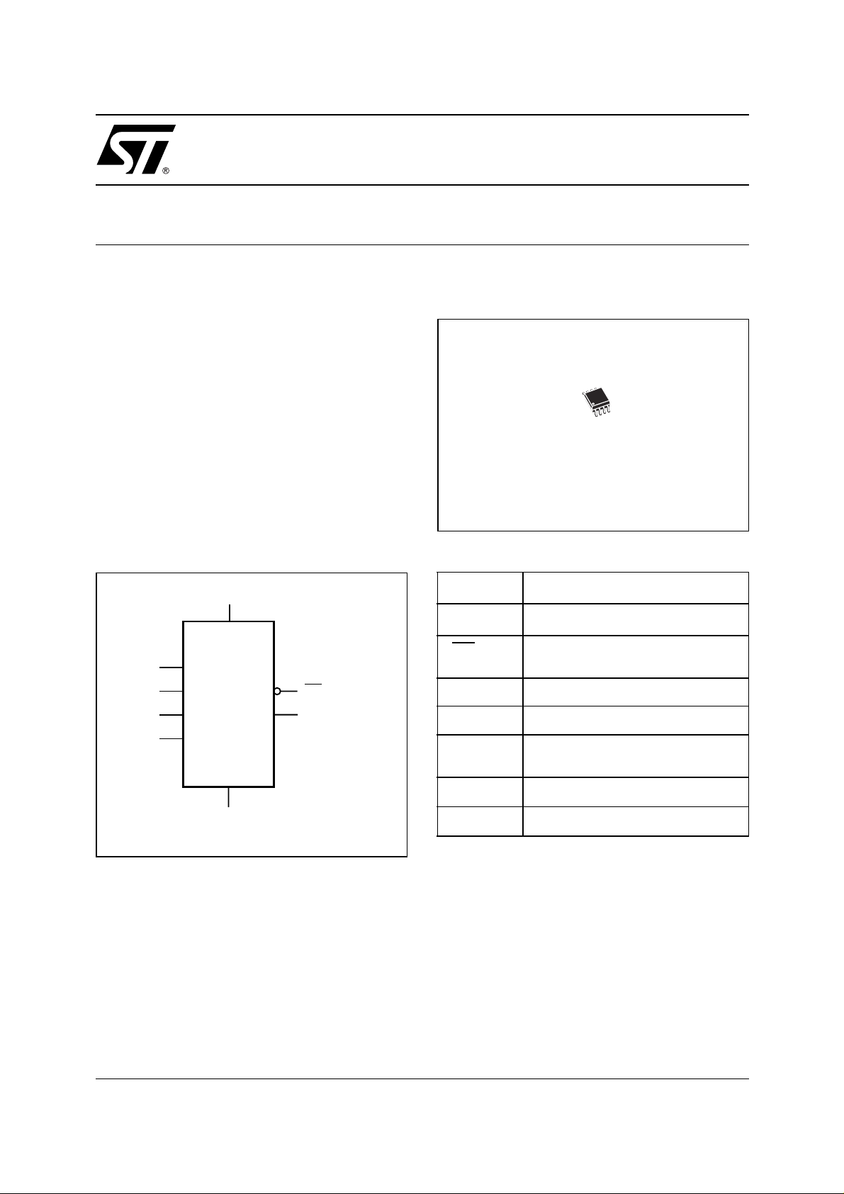
M41T80
Figure 2. 8-pi n S OI C Package
8
1
SO8 (M)
Figure 1. Logic Diagram
V
CC
XI
XO
SCL
SDA
M41T80
V
SS
IRQ/OUT/SQW
F
32k
AI07005
Table 1. Signal Names
XI
XO
IRQ
/OUT/
SQW
SDA Serial Data Input/Output
SCL Serial Clock Input
F
32k
V
CC
V
SS
Oscillator Input
Oscillator Output
Interrupt / Output Driver / Square
Wave (Open Drain)
32kHz Square Wave Output (Open
drain)
Supply Voltage
Ground
1/20October 2002

M41T80
TABLE OF CONTENTS
SUMMARY DESCRIPTION. . . . . . . . . . . . . . . . . . . . . . . . . . . . . . . . . . . . . . . . . . . . . . . . . . . . . . . . . . . 3
8-pin SOIC Connections (Figure 3.) . . . . . . . . . . . . . . . . . . . . . . . . . . . . . . . . . . . . . . . . . . . . . . . . . 3
Block Diagram (Fi g ure 4 .) . . . . . . . . . . . . . . . . . . . . . . . . . . . . . . . . . . . . . . . . . . . . . . . . . . . . . . . . . 3
MAXIMUM RATING. . . . . . . . . . . . . . . . . . . . . . . . . . . . . . . . . . . . . . . . . . . . . . . . . . . . . . . . . . . . . . . . . 4
Absolute Maximum Rati ng s (Table 2.) . . . . . . . . . . . . . . . . . . . . . . . . . . . . . . . . . . . . . . . . . . . . . . .4
DC AND AC PARAMETERS. . . . . . . . . . . . . . . . . . . . . . . . . . . . . . . . . . . . . . . . . . . . . . . . . . . . . . . . . . 5
Operating and AC Measurement Conditions (Table 3.) . . . . . . . . . . . . . . . . . . . . . . . . . . . . . . . . . . 5
AC Measurement I/O Waveform (Figure 5.) . . . . . . . . . . . . . . . . . . . . . . . . . . . . . . . . . . . . . . . . . . . 5
Capacitance (Table 4.) . . . . . . . . . . . . . . . . . . . . . . . . . . . . . . . . . . . . . . . . . . . . . . . . . . . . . . . . . . . 5
DC Characteristi cs (Table 5.) . . . . . . . . . . . . . . . . . . . . . . . . . . . . . . . . . . . . . . . . . . . . . . . . . . . . . . 6
Crystal Electrical Characteristics (Table 6.). . . . . . . . . . . . . . . . . . . . . . . . . . . . . . . . . . . . . . . . . . . . 6
OPERATION . . . . . . . . . . . . . . . . . . . . . . . . . . . . . . . . . . . . . . . . . . . . . . . . . . . . . . . . . . . . . . . . . . . . . . 7
2-Wire Bus Characteristics . . . . . . . . . . . . . . . . . . . . . . . . . . . . . . . . . . . . . . . . . . . . . . . . . . . . . . . . 7
Serial Bus Data Transfer Sequence (Figure 6.) . . . . . . . . . . . . . . . . . . . . . . . . . . . . . . . . . . . . . . . .8
Acknowledgement Sequ ence (Figure 7.) . . . . . . . . . . . . . . . . . . . . . . . . . . . . . . . . . . . . . . . . . . . . . 8
Bus Timing Requirements Sequence (Figure 8.) . . . . . . . . . . . . . . . . . . . . . . . . . . . . . . . . . . . . . . . 9
AC Characteristics (Table 7.) . . . . . . . . . . . . . . . . . . . . . . . . . . . . . . . . . . . . . . . . . . . . . . . . . . . . . . 9
READ Mode. . . . . . . . . . . . . . . . . . . . . . . . . . . . . . . . . . . . . . . . . . . . . . . . . . . . . . . . . . . . . . . . . . . 1 0
Slave Address Location (Figure 9.). . . . . . . . . . . . . . . . . . . . . . . . . . . . . . . . . . . . . . . . . . . . . . . . . 10
READ Mode Sequence (Figure 10.) . . . . . . . . . . . . . . . . . . . . . . . . . . . . . . . . . . . . . . . . . . . . . . . . 10
Alternative READ Mode Sequence (Figure 11.) . . . . . . . . . . . . . . . . . . . . . . . . . . . . . . . . . . . . . . .11
WRITE Mode. . . . . . . . . . . . . . . . . . . . . . . . . . . . . . . . . . . . . . . . . . . . . . . . . . . . . . . . . . . . . . . . . . 11
WRITE Mode Sequence (Figure 12.) . . . . . . . . . . . . . . . . . . . . . . . . . . . . . . . . . . . . . . . . . . . . . . . 11
CLOCK OPERATION . . . . . . . . . . . . . . . . . . . . . . . . . . . . . . . . . . . . . . . . . . . . . . . . . . . . . . . . . . . . . . 12
TIMEKEEPER® Registers. . . . . . . . . . . . . . . . . . . . . . . . . . . . . . . . . . . . . . . . . . . . . . . . . . . . . . . . 12
TIMEKEEPER® Register Map (Table 8.) . . . . . . . . . . . . . . . . . . . . . . . . . . . . . . . . . . . . . . . . . . . . 13
Full-time 32kHz Square Wave Output . . . . . . . . . . . . . . . . . . . . . . . . . . . . . . . . . . . . . . . . . . . . . . .15
Century Bit. . . . . . . . . . . . . . . . . . . . . . . . . . . . . . . . . . . . . . . . . . . . . . . . . . . . . . . . . . . . . . . . . . . . 16
Alarm Interrupt Reset Waveform (Figure 13.) . . . . . . . . . . . . . . . . . . . . . . . . . . . . . . . . . . . . . . . . . 14
Alarm Repeat Modes (Table 9.) . . . . . . . . . . . . . . . . . . . . . . . . . . . . . . . . . . . . . . . . . . . . . . . . . . . 14
Square Wave Output Frequency (Table 10.). . . . . . . . . . . . . . . . . . . . . . . . . . . . . . . . . . . . . . . . . . 15
Century Bit. . . . . . . . . . . . . . . . . . . . . . . . . . . . . . . . . . . . . . . . . . . . . . . . . . . . . . . . . . . . . . . . . . . . 16
Output Driver Pin. . . . . . . . . . . . . . . . . . . . . . . . . . . . . . . . . . . . . . . . . . . . . . . . . . . . . . . . . . . . . . . 16
Preferred Power-on Def a ult. . . . . . . . . . . . . . . . . . . . . . . . . . . . . . . . . . . . . . . . . . . . . . . . . . . . . . . 16
Preferred Power-on Def a ult Values (Table 11.) . . . . . . . . . . . . . . . . . . . . . . . . . . . . . . . . . . . . . . . 16
PART NUMBERING . . . . . . . . . . . . . . . . . . . . . . . . . . . . . . . . . . . . . . . . . . . . . . . . . . . . . . . . . . . . . . . 17
PACKAGE MECHANICAL INFORMATION . . . . . . . . . . . . . . . . . . . . . . . . . . . . . . . . . . . . . . . . . . . . . 18
REVISION HISTORY. . . . . . . . . . . . . . . . . . . . . . . . . . . . . . . . . . . . . . . . . . . . . . . . . . . . . . . . . . . . . . . 19
2/20
M41T80
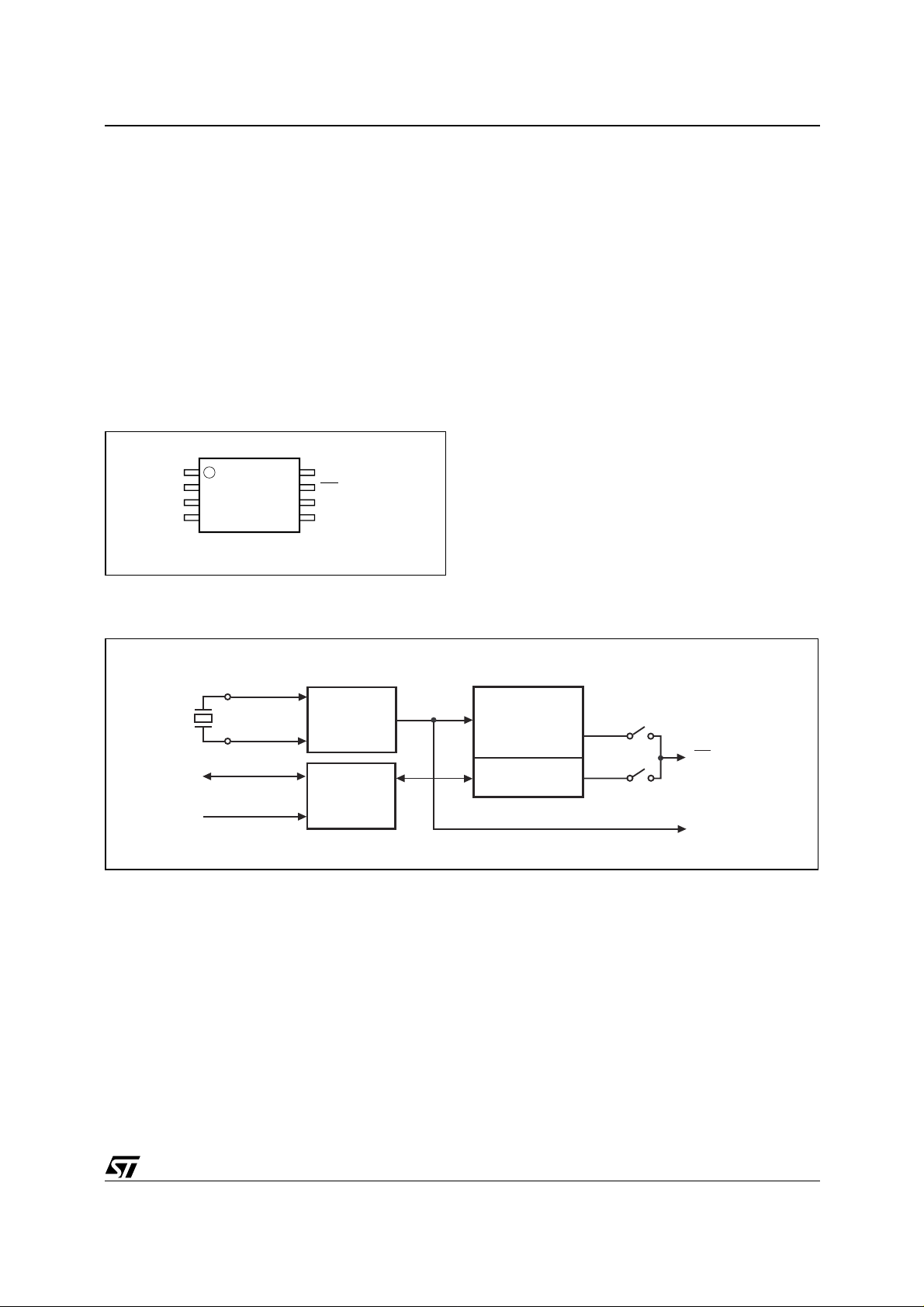
SUMMARY DESCRIPTION
The M41T80 Serial Access TIMEKEEPER
SRAM is a low power Serial RTC with a built-in
32.768 KHz oscillator (external crystal controlled).
Eight registers (see Table 8, page 13) are used for
the clock/calendar func tion and a re configured in
binary coded decimal (BCD) format. An additional
12 registers provide status/control of Alarm, 32kHz
output, and Square Wave functions. Addresses
and data are transferred se rially via a t wo li ne, bidirectional I
2
C interface. The built-in address register is incremented automatically after each
WRITE or READ data byte.
Figure 3. 8-pin SOIC Connections
V
1
XI
2
XO
(1)
F
32k
V
SS
Note: 1. Open drain output.
M41T80
3
45
8
CC
7
IRQ/OUT/SQW
6
SCL
SDA
(1)
AI07006
®
Functions available to the user include a time-ofday clock/calendar, Alarm interrup ts, 32kHz output, and programmable Square Wave output. The
eight clock address locations contain the cent ury,
year, month, date, day, hour, minute, second and
tenths/hundredths of a second in 24 hour BCD format. Corrections for 28, 29 (leap yea r - valid until
year 2100), 30 and 31 day months are made automatically.
The M41T80 is supplied in an 8-pin SOIC.
Figure 4. Block Diagram
CRYSTAL
SDA
SCL
Note: 1. Open Drain output
32KHz
OSCILLATOR
I2C
INTERFACE
REAL TIME CLOCK
CALENDAR
RTC W/ALARM
SQUARE WAVE
AF
IRQ/OUT/SQW
(1)
F
32k
AI07007
(1)
3/20
M41T80
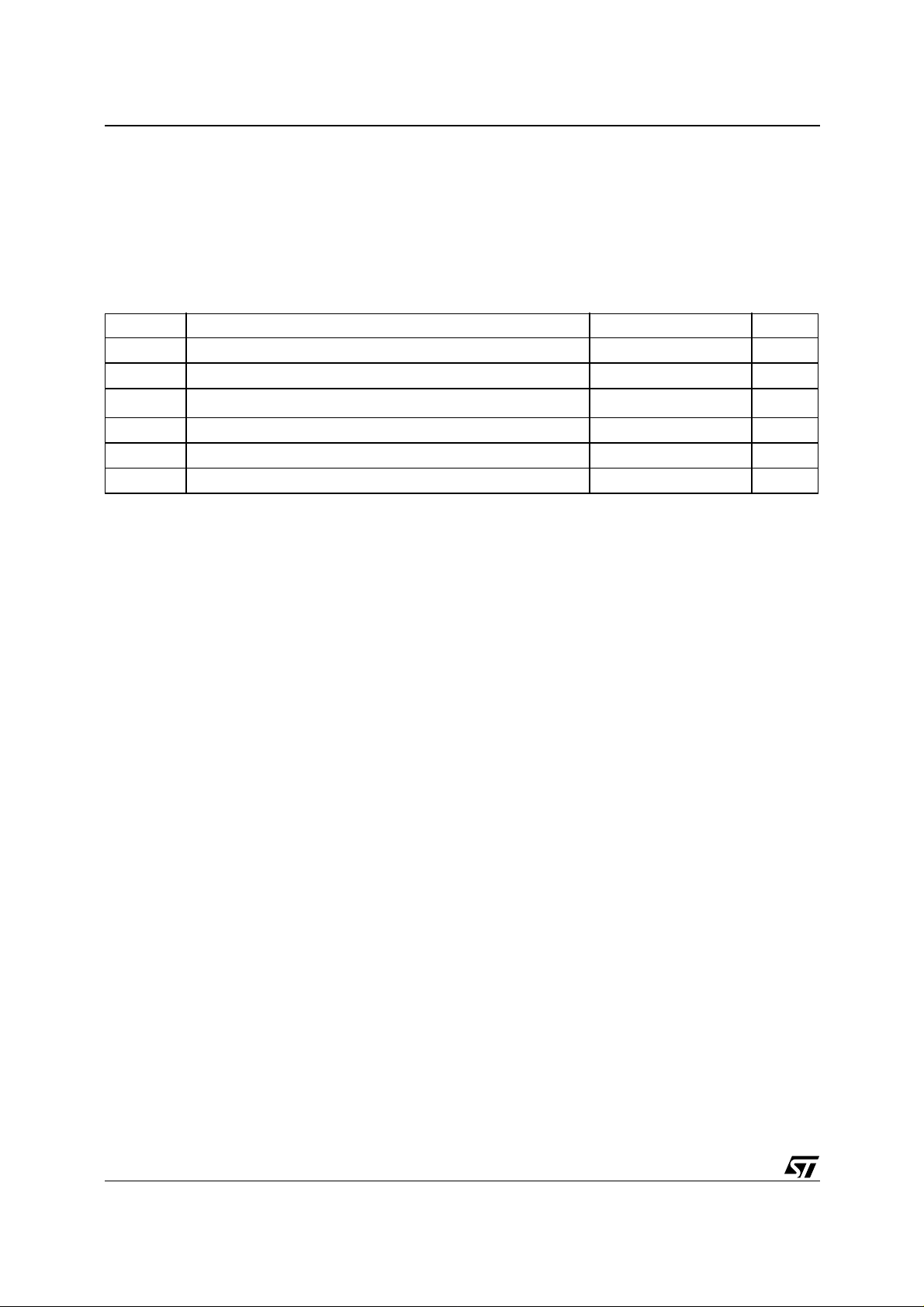
MAXIMUM RATIN G
Stressing the device above the rating l isted in the
“Absolute Maximum Ratings” table may cause
permanent damage to the device. These are
stress ratings only and operation of the dev ice at
these or any other conditions above those indicated in the Operating sections of this specification is
Table 2. Absolute Maximum Ratings
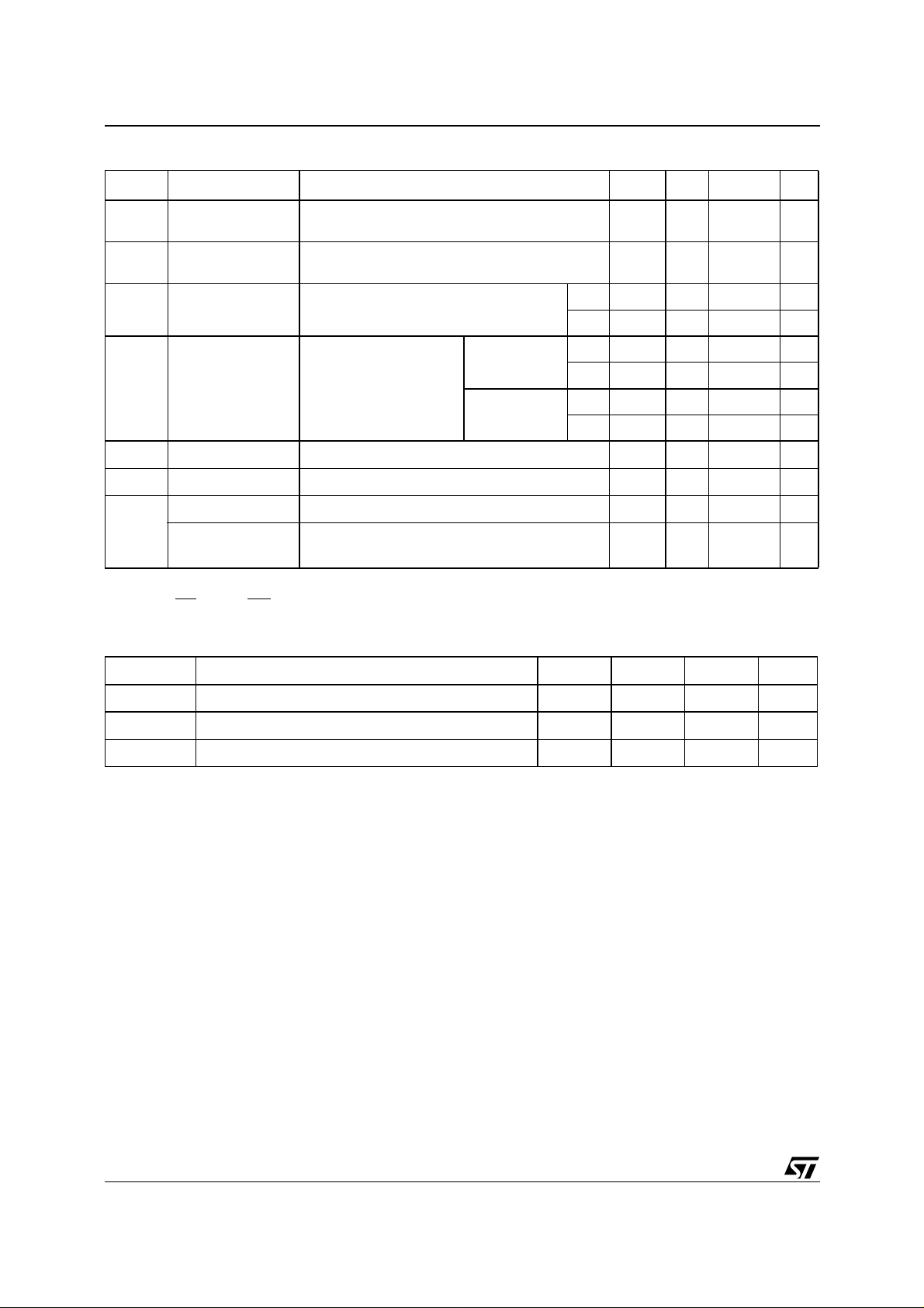
Sym Parameter Value Unit
T
STG
V
CC
T
SLD
V
IO
I
O
P
Note: 1. Reflow at peak temperature of 215°C to 225°C for < 60 sec onds (total thermal budg et not to exce ed 180°C for bet ween 90 to 12 0
Storage Temperature (VCC Off, Oscillator Off)
Supply Voltage –0.3 to 7 V
(1)
Lead Solder Temperature for 10 Seconds 260 °C
Input or Output Voltages –0.3 to Vcc+0.3 V
Output Current 20 mA
Power Dissipation 1 W
D
secon ds).
not implied. Exposure to Absol ute Maxim um Rating conditions for extended periods may affect device reliability. Refer also to the
STMicroelectronics SURE Program and oth er relevant quality documents.
–55 to 125
°C
4/20
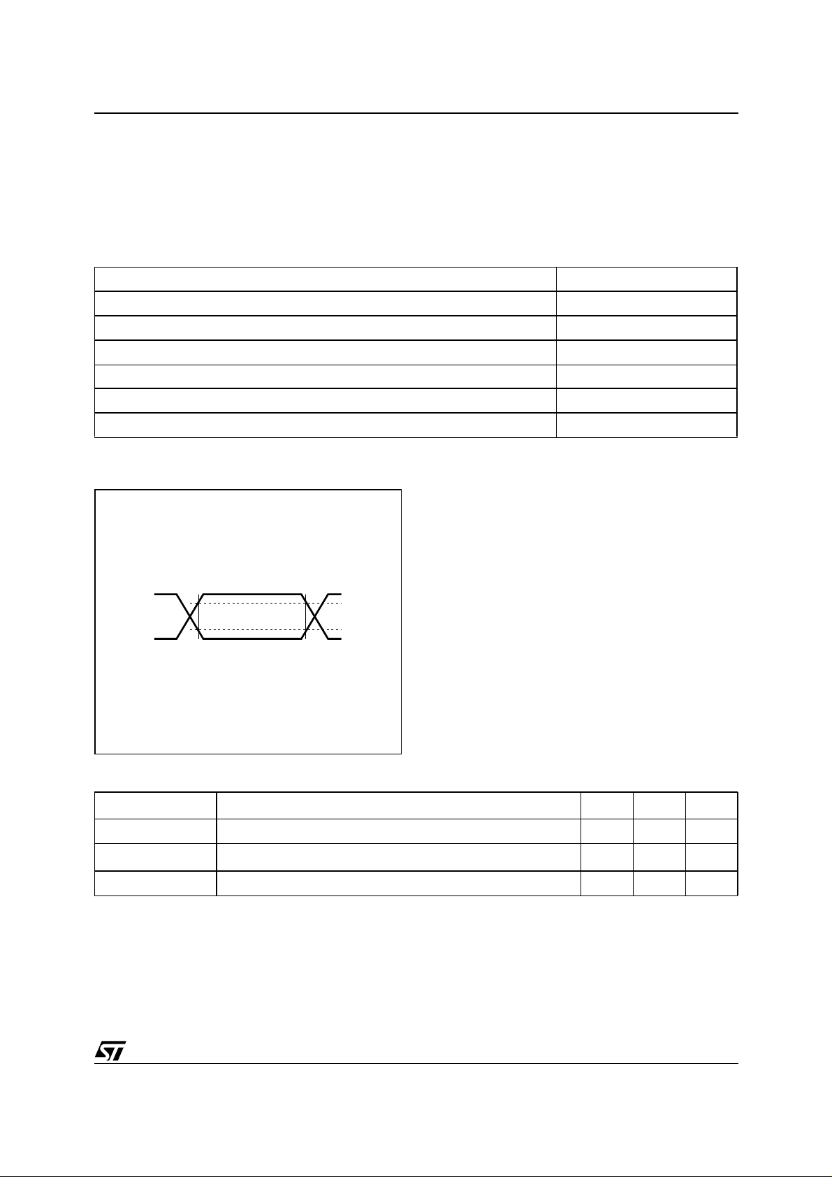
DC AND AC PARAMETERS
This section summarizes the operat ing and measurement conditions, as well as the DC and AC
characteristics of the device. The parameters in
the following DC and AC Characteristic tables are
derived from tests performed under the M easure-
Table 3. Operating and AC Measurement Conditions
Parameter M41T80
M41T80
ment Conditions listed i n the relevant tables. Designers should check that the operating conditions
in their projects match the measurement conditions when using the quoted parameters.
Supply Voltage (V
Ambient Operating Temperature (T
Load Capacitance (C
CC
)
)
A
)
L
2.0 to 5.5V
–40 to 85°C
100pF
Input Rise and Fall Times ≤ 50ns
0.2V
0.3V
to 0.8 V
CC
to 0.7 V
CC
Input Pulse Voltages
Input and Output Timing Ref. Voltages
Note: Output Hi -Z is define d as the point wh ere data is no longer driven.
Figure 5. AC Measurement I/O Waveform
0.8V
0.2V
CC
CC
0.7V
0.3V
AI02568
CC
CC
CC
CC
Table 4. Capacitance
Symbol
C
IN
(3)
C
OUT
t
LP
Note: 1. Effective capacitance measured with power suppl y at 5V; sampled only, not 100% tested.
2. At 25°C, f = 1MHz.
3. Outputs deselected .
Input Capacitance 7 pF
Output Capacitance 10 pF
Low-pass filter input time constant (SDA and SCL) 50 ns
Parameter
(1,2)
Min Max Unit
5/20
M41T80
Table 5. DC Characteristics
Symbol Parameter
Input Leakage
I
LI
Current
Output Leakage
I
LO
Current
I
CC2
I
Supply Current Switch Freq (SCL) = 400kHz
CC1
Supply Current
(2)
(standby)
V
Input Low Voltage –0.3
IL
V
Input High Voltage
IH
All Inputs = V
Switch Freq (SCL) = 0Hz
Output Low Voltage
V
OL
Output Low Voltage
(Open Drain)
Note: 1. Valid for Am bi ent Operat in g T em perature : TA = –40 to 85°C ; VCC = 2.0 to 5.5V (except where noted).
2. At 25°C.
3. For IRQ
/FT/OUT, RST, and 32kHz pins (Open Drain)
(3)
Test Condition
0V ≤ V
0V ≤ V
OUT
– 0.2V
CC
I
= 3.0mA 0.4
OL
IOL = 10mA
(1)
≤ V
IN
CC
≤ V
CC
32KE = 1
or SQWE = 1
32KE = 0
and SQWE = 0
Min Typ Max Unit
3.0V 30 µA
5.5V 200 µA
3.0V 1.8 3.0 µA
5.5V 35 µA
3.0V 1.5 2.4 µA
5.5V 31 µA
0.7V
CC
±1 µA
±1 µA
0.3V
CC
VCC + 0.3
0.4 V
V
V
V
Table 6. Crystal Electrical Characteristics
Sym
f
O
R
S
C
L
Note: 1. Externally s uppl ied i f us ing th e S O8 pa ckag e. STM icroe lec troni cs reco mm ends the K DS DT -38: 1TA/ 1TC 252E 127, Tun ing Fork
Type (thru-hole) or the DMX-26S: 1TJS125FH2A212, (SMD) quartz crystal for industrial temperature operations. KDS can be contacted at kouhou@kdsj .c o.jp or http ://www.kds j .c o.jp for further inform at i on on this crystal type.
2. Load capacitors are integrated within the M41T80. Circuit board layout considerations for the 32.768 kHz crystal of minimum trace
lengths an d i solation from RF generating signals should be taken into account.
Resonant Frequency 32.768 kHz
Series Resistance 60 kΩ
Load Capacitance 12.5 pF
Parameter
(1,2)
Min Typ Max Units
6/20
 Loading...