

SGS Thomson Microelectronics M41T56SH6TR, M41T56MH6TR, M41T56M6TR Datasheet
1/23November 2002
M41T56
512 bit (64 bit x 8) SERIAL ACCESS TIMEKEEPER® SRAM
FEATURES SUMMARY
■ 5V ±10% SUPPL Y VO L TAG E
■ COUNTERS FOR SECONDS, MINUTES,
HOURS, DAY, DATE, MONT H , YEAR S, and
CENTURY
■ YEAR 2000 COMPLIANT
■ SOFTWARE CLOCK CALIBRATION
■ AUTOMATIC POWER-FAIL DETECT and
SWITCH CIRCUITRY
■ I
2
C BUS C O MPATI BLE
■ 56 BYTES OF GENERAL PURPOSE RAM
■ ULTRA-LOW BATTER Y SUPPLY CURRENT
OF 450nA
■ LOW OPERATING CURRENT OF 300µA
■ OPERATING TEMPER ATURE OF –40 to 85°C
■ AUTOMATIC LEAP YEAR COMPENSATION
■ SPECIAL SOFT WARE PROGRAM MABLE
OUTPUT
■ PACKA GING OP TIONS IN CLUDE :
– 28-LEAD SOIC and SNAPHA T
®
TOP
(to be Ordered Separately)
–SO8
Figure 1. 8-pi n S OI C Package
Figure 2. 28-pi n S O I C Package
8
1
SO8 (M)
150mil Width
28
1
SOH28 (MH)
SNAPHAT (SH)
Battery & Crystal

M41T56
2/23
TABLE OF CONTENTS
SUMMARY DESCRIPTION. . . . . . . . . . . . . . . . . . . . . . . . . . . . . . . . . . . . . . . . . . . . . . . . . . . . . . . . . . . 3
Logic Diagram ( Fig u r e 3.) . . . . . . . . . . . . . . . . . . . . . . . . . . . . . . . . . . . . . . . . . . . . . . . . . . . . . . . . . 3
Signal Names (Table 1.) . . . . . . . . . . . . . . . . . . . . . . . . . . . . . . . . . . . . . . . . . . . . . . . . . . . . . . . . . . 3
8-pin SOIC Connections (Figure 4.) . . . . . . . . . . . . . . . . . . . . . . . . . . . . . . . . . . . . . . . . . . . . . . . . . 4
28-pin SOIC Connection s (Figure 5.) . . . . . . . . . . . . . . . . . . . . . . . . . . . . . . . . . . . . . . . . . . . . . . . . 4
Block Diagram (Fi g ure 6 .) . . . . . . . . . . . . . . . . . . . . . . . . . . . . . . . . . . . . . . . . . . . . . . . . . . . . . . . . . 4
MAXIMUM RATING. . . . . . . . . . . . . . . . . . . . . . . . . . . . . . . . . . . . . . . . . . . . . . . . . . . . . . . . . . . . . . . . . 5
Absolute Maximum Rati ng s (Table 2.) . . . . . . . . . . . . . . . . . . . . . . . . . . . . . . . . . . . . . . . . . . . . . . .5
DC AND AC PARAMETERS. . . . . . . . . . . . . . . . . . . . . . . . . . . . . . . . . . . . . . . . . . . . . . . . . . . . . . . . . . 6
Operating and AC Measurement Conditions (Table 3.) . . . . . . . . . . . . . . . . . . . . . . . . . . . . . . . . . .6
AC Measurement I/O Waveform (Figure 7.) . . . . . . . . . . . . . . . . . . . . . . . . . . . . . . . . . . . . . . . . . . . 6
Capacitance (Table 4.) . . . . . . . . . . . . . . . . . . . . . . . . . . . . . . . . . . . . . . . . . . . . . . . . . . . . . . . . . . . 6
DC Characteristi cs (Table 5.) . . . . . . . . . . . . . . . . . . . . . . . . . . . . . . . . . . . . . . . . . . . . . . . . . . . . . . 7
Crystal Electrical Characteristics (Table 6.). . . . . . . . . . . . . . . . . . . . . . . . . . . . . . . . . . . . . . . . . . . . 7
OPERATION . . . . . . . . . . . . . . . . . . . . . . . . . . . . . . . . . . . . . . . . . . . . . . . . . . . . . . . . . . . . . . . . . . . . . . 8
2-Wire Bus Characteristics . . . . . . . . . . . . . . . . . . . . . . . . . . . . . . . . . . . . . . . . . . . . . . . . . . . . . . . . 8
Serial Bus Data Transfer Sequence (Figure 8.) . . . . . . . . . . . . . . . . . . . . . . . . . . . . . . . . . . . . . . . .9
Acknowledge Sequence (Figure 9.) . . . . . . . . . . . . . . . . . . . . . . . . . . . . . . . . . . . . . . . . . . . . . . . . . 9
Bus Timing Requirements Sequence (Figure 10.) . . . . . . . . . . . . . . . . . . . . . . . . . . . . . . . . . . . . . . 9
AC Characteristics (Table 7.) . . . . . . . . . . . . . . . . . . . . . . . . . . . . . . . . . . . . . . . . . . . . . . . . . . . . . 10
READ Mode. . . . . . . . . . . . . . . . . . . . . . . . . . . . . . . . . . . . . . . . . . . . . . . . . . . . . . . . . . . . . . . . . . . 10
WRITE Mode. . . . . . . . . . . . . . . . . . . . . . . . . . . . . . . . . . . . . . . . . . . . . . . . . . . . . . . . . . . . . . . . . . 12
Slave Address Location (Figure 11.). . . . . . . . . . . . . . . . . . . . . . . . . . . . . . . . . . . . . . . . . . . . . . . . 1 0
READ Mode Sequence (Figure 12.) . . . . . . . . . . . . . . . . . . . . . . . . . . . . . . . . . . . . . . . . . . . . . . . . 11
Alternative READ Mode Sequence (Figure 13.) . . . . . . . . . . . . . . . . . . . . . . . . . . . . . . . . . . . . . . . 11
WRITE Mode Sequence (Figure 14.) . . . . . . . . . . . . . . . . . . . . . . . . . . . . . . . . . . . . . . . . . . . . . . . 12
Data Retention Mode. . . . . . . . . . . . . . . . . . . . . . . . . . . . . . . . . . . . . . . . . . . . . . . . . . . . . . . . . . . . 13
Power Down/Up Mode AC Waveforms (Figure 15.) . . . . . . . . . . . . . . . . . . . . . . . . . . . . . . . . . . . . 13
Power Down/Up Mode AC Characteristics (Table 8.) . . . . . . . . . . . . . . . . . . . . . . . . . . . . . . . . . . . 13
Power Down/Up Trip Points DC Char ac te r i stics (Table 9.). . . . . . . . . . . . . . . . . . . . . . . . . . . . . . . 13
CLOCK OPERATION . . . . . . . . . . . . . . . . . . . . . . . . . . . . . . . . . . . . . . . . . . . . . . . . . . . . . . . . . . . . . . 14
Register Map (Table 10.). . . . . . . . . . . . . . . . . . . . . . . . . . . . . . . . . . . . . . . . . . . . . . . . . . . . . . . . . 14
Clock Calibratio n. . . . . . . . . . . . . . . . . . . . . . . . . . . . . . . . . . . . . . . . . . . . . . . . . . . . . . . . . . . . . . . 1 5
Output Driver Pin. . . . . . . . . . . . . . . . . . . . . . . . . . . . . . . . . . . . . . . . . . . . . . . . . . . . . . . . . . . . . . . 1 5
Initial Power- o n Defaults . . . . . . . . . . . . . . . . . . . . . . . . . . . . . . . . . . . . . . . . . . . . . . . . . . . . . . . . . 15
Crystal Accuracy Across Temperature (Figure 16.) . . . . . . . . . . . . . . . . . . . . . . . . . . . . . . . . . . . . 16
Clock Calibratio n (Figure 17.) . . . . . . . . . . . . . . . . . . . . . . . . . . . . . . . . . . . . . . . . . . . . . . . . . . . . . 1 6
PART NUMBERING . . . . . . . . . . . . . . . . . . . . . . . . . . . . . . . . . . . . . . . . . . . . . . . . . . . . . . . . . . . . . . . 17
SNAPHAT Battery/Crystal Table (Table 12.). . . . . . . . . . . . . . . . . . . . . . . . . . . . . . . . . . . . . . . . . . 17
PACKAGE MECHANICAL INFORMATION . . . . . . . . . . . . . . . . . . . . . . . . . . . . . . . . . . . . . . . . . . . . . 18
REVISION HISTORY . . . . . . . . . . . . . . . . . . . . . . . . . . . . . . . . . . . . . . . . . . . . . . . . . . . . . . . . . . . . . . . 22
3/23
M41T56
SUMMARY DESCRIPTION
The M41T56 TIMEKEEPER
®
is a low power, 512bit static CMOS RAM organized as 64 words by 8
bits. A built-in 32,768 Hz oscillator (external crystal
controlled) and the first 8 bytes of the RAM are
used for the clock/calendar function and are configured in binary coded decimal (BCD) format. Addresses and data are transferred serially via a twoline, bi-directional bus. The built-in address register is incremented automatically after each WRITE
or READ data byte.
The M41T56 clock has a built-in power sense circuit which detects power failures and automatically switches to the battery supply during power
failures. The energy needed to sustain the RAM
and clock operations can be supplied from a small
lithium co in cel l.
Typical data retention time is in excess of 10 years
with a 50mAh, 3V lithium cell. The M41T56 is supplied in an 8-lead P lastic SOIC package or a 28lead SNAPHAT
®
package.
The 28-pin, 330mil SOIC provides sockets with
gold plated contacts at both ends for direct connection to a separate SNAPHAT housing cont aining the battery and crystal. The unique design
allows the SNAPHAT battery package to be
mounted on top of the SOIC package after the
completion of the surface mount process. Insertion of the SNAPHAT housing after reflow prevents potential battery and c rystal dam age d ue t o
the high temperatures required for device surfacemounting. The SNAPHAT housing is keyed to prevent reverse insertion. The SOIC and battery/crystal packages are shipped separately in plastic antistatic tubes or in Tape & Reel form.
For the 28-lead SOIC, the battery/crystal package
(e.g., SNAPHAT) part number is “M4TxxBR12SH” (see Table 12, page 17).
Caution: Do not place the SNAPHAT battery/crystal package “M4Txx-BR12SH” i n condu ctive foam
as this will drain the lithium button-cell battery.
Figure 3. Logic Diagram Table 1. Signal Names
AI02304B
OSCI
V
CC
M41T56
V
SS
SCL
OSCO
SDA
FT/OUT
V
BAT
OSCI Oscillator Input
OCSO Oscillator Output
FT/OUT
Frequency Test / Output Driver
(Open Drain)
SDA Serial Data Address Input / Output
SCL Serial Clock
V
BAT
Battery Supply Voltage
V
CC
Supply Voltage
V
SS
Ground
M41T56
4/23
Figure 4. 8-pi n S OI C Co nn e ct io ns Figure 5. 28-pi n S O I C C onnections
Figure 6. Block Diagram
1
SDAV
SS
SCL
FT/OUTOSCO
OSCI V
CC
V
BAT
AI02306B
M41T56
2
3
4
8
7
6
5
AI03607
8
2
3
4
5
6
7
9
10
11
12
13
14
22
21
20
19
18
17
16
15
28
27
26
25
24
23
1
NC
V
SS
NC
NC
NC V
CC
M41T56
NC
NC
NC
NC
NC
NC
NC
NC
NC
NC
NC
SDA
NC
SCL
NC
NC
NC
NC
NC
FT/OUT
NC
NC
AI02566
SECONDS
OSCILLATOR
32.768 kHz
VOLTAGE
SENSE
and
SWITCH
CIRCUITRY
SERIAL
BUS
INTERFACE
DIVIDER
CONTROL
LOGIC
ADDRESS
REGISTER
MINUTES
CENTURY/HOURS
DAY
DATE
MONTH
YEAR
CONTROL
RAM
(56 x 8)
OSCI
OSCO
FT/OUT
V
CC
V
SS
V
BAT
SCL
SDA
1 Hz
5/23
M41T56
MAXIMUM RATING
Stressing the device above the rating listed in t he
“Absolute Maximum Ratings” table may cause
permanent damage to the device. These are
stress ratings only and operation of the dev ice at
these or any other conditions above those indicated in the Operating sections of this specification is
not implied. Exposure to Absol ute Maxim um Rating conditions for extended periods may affect device reliability. Refer also to the
STMicroelectronics SURE Program and oth er relevant quality documents.
Table 2. Absolute Maximum Ratings
Note: 1. Reflow at peak temperature of 215°C to 225°C for < 60 seconds (total thermal budget not to exceed 180°C for between 90 and 120
seconds).
CAUTION: Nega tive undershoot s below –0.3V are not allowed on any pi n while in the Bat tery Back-up mode.
CAUTION: Do NOT wav e s older SOI C t o avoid da m ag i ng SNAP HAT so c kets.
Symbol Parameter Value Unit
T
A
Ambient Operating Temperature –40 to 85 °C
T
STG
Storage Temperature (VCC Off, Oscillator Off)
SNAPHAT –40 to 85
°C
SOIC –55 to 125
T
SLD
(1)
Lead Solder Temperature for 10 seconds 260 °C
V
IO
Input or Output Voltages –0.3 to 7 V
V
CC
Supply Voltage –0.3 to 7 V
I
O
Output Current 20 mA
P
D
Power Dissipation 0.25 W
M41T56
6/23
DC AND AC PARAMETERS
This section summarizes the operat ing and measurement conditions, as well as the DC and AC
characteristics of the device. The parameters in
the following DC and AC Characteristic tables are
derived from tests performed under the M easure-
ment Conditions listed i n the relevant tables. Designers should check that the operating conditions
in their projects match the measurement conditions when using the quoted parameters.
Table 3. Operating and AC Measurement Conditions
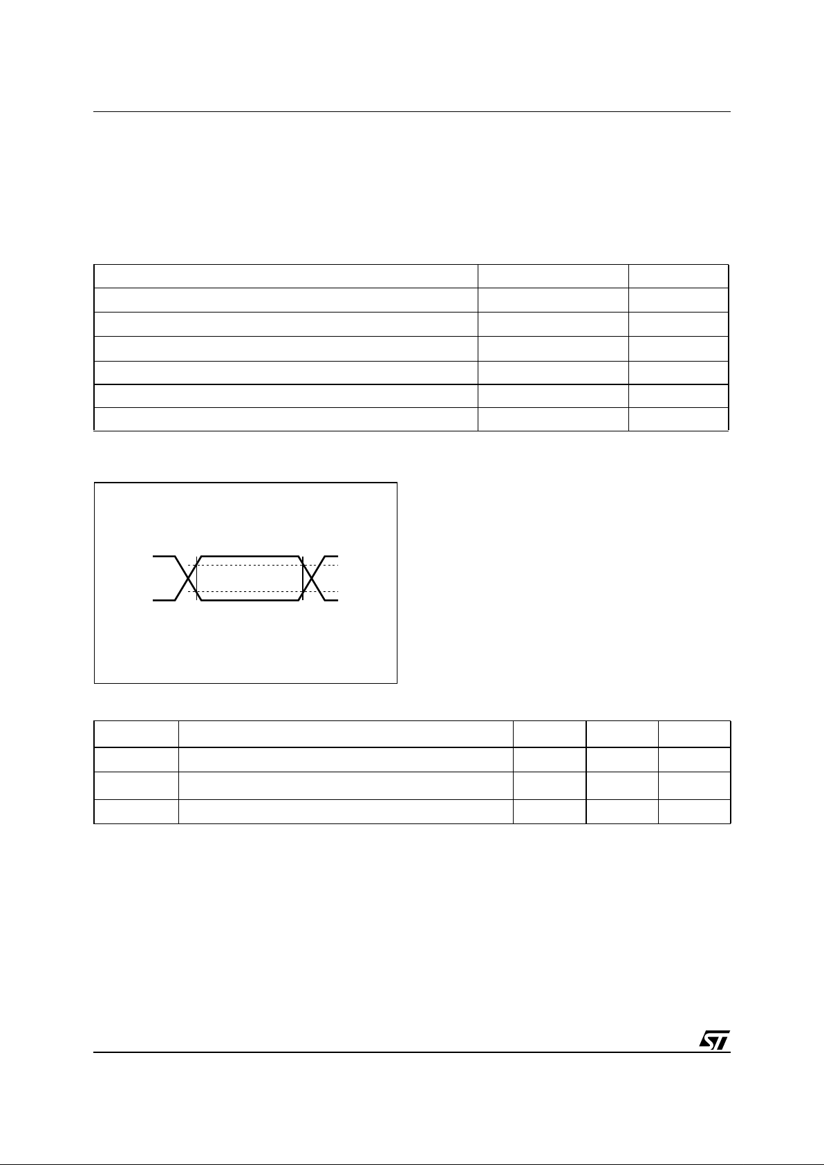
Note: Output Hi-Z is def i ned as the point where data is no longer driven.
Figure 7. AC Measurement I/O Waveform
Table 4. Capacitance
Note: 1. Eff ective capacitance measured with powe r supply at 5V; sam p l ed, not 100% tested.
2. At 25°C, f = 1M Hz.
3. Outputs desele ct ed.
Parameter Value Unit
Supply Voltage (V
CC
)
4.5 to 5.5 V
Ambient Operating Temperature (T
A
)
–40 to 85 °C
Load Capacitance (C
L
)
100 pF
Input Rise and Fall Times ≤ 5ns
Input Pulse Voltages 0 to 3 V
Input and Output Timing Ref. Voltages 1.5 V
AI02568
0.8V
CC
0.2V
CC
0.7V
CC
0.3V
CC
Symbol
Parameter
(1,2)
Min Max Unit
C
IN
Input Capacitance (SCL) 7 pF
C
OUT
(3)
Output Capacitance (SDA, FT/OUT) 10 pF
t
LP
Low-pass filter input time constant (SDA and SCL) 0.25 1 µs
7/23
M41T56
Table 5. DC Characteristics
Note: 1. Val i d for Ambient Operating Temperature: TA = –40 to 85°C ; VCC = 4.5 to 5.5V (except where noted).
2. STMicroelectronics rec ommends the R AYOVAC BR1225 or BR1632 (or eq ui valent) as the ba tt ery supply.
Table 6. Crystal Electrical Characteristics
Note: 1. These values are externally supplied if using the SO8 package. STMicroelectronics recommends the KDS DT-38: 1TA/
1TC252E1 27, Tunin g Fo rk T ype (thr u- hole ) or t he D MX- 26 S: 1T JS1 25FH2A 2 12, ( SMD) qu artz cry stal for i ndus tri al temper at ure
operation s. KDS can be contacted at kouhou@kdsj.co.jp or htt p://www.kdsj.co.jp for furt her informat i on on this crystal ty pe.
2. Load capacitors are integrated within the M41T56. Circuit board layout considerations for the 32.768 kHz crystal of minimum trace
lengths an d i solation from RF generating sig nal s should be taken into accoun t.
3. All SNAPHAT battery/cry stal tops meet these specifica tions.
Symbol Parameter
Test Condition
(1)
Min Typ Max Unit
I
LI
Input Leakage Current
0V ≤ V
IN
≤ V
CC
±1 µA
I
LO
Output Leakage Current
0V ≤ V
OUT
≤ V
CC
±1 µA
I
CC1
Supply Current Switch Frequency = 100kHz 300 µA
I
CC2
Supply Current (Standby)
SCL, SDA = V
CC
– 0.3V
100 µA
V
IL
Input Low Voltage –0.3 1.5 V
V
IH
Input High Voltage 3
V
CC
+ 0.8
V
V
OL
Output Low Voltage
I
OL
= 5mA, VCC = 4.5V
0.4 V
V
BAT
(2)
Battery Supply Voltage 2.5 3 3.5 V
I
BAT
Battery Supply Current
T
A
= 25°C, VCC = 0V,
Oscillator ON, V
BAT
= 3V
450 550 nA
Symbol
Parameter
(1,2,3)
Min Typ Max Unit
f
O
Resonant Frequency 32.768 kHz
R
S
Series Resistance 60 kΩ
C
L
Load Capacitance 12.5 pF
 Loading...