

512 bit (64b x8) Serial Access TIMEKEEPER® SRAM
■ 5V ±10% SUPPLY VOLTAG E
■ COUNTERS for SECONDS, MINUTES,
HOURS, DAY, DATE , MONTH, YEARS and
CENTURY
■ YEAR 2000 COMPLIANT
■ SOFTWARE CLOCK CALIBRATION
■ AUTOMATIC POWER-FAIL DETECT and
SWITCH CIRCUITRY
2
■ I
C BUS C O MPATI BLE
■ 56 BYTES of GENERAL PURPOSE RAM
■ ULTRA-LOW BATTER Y SU PPL Y CU RRE N T
of 500nA
■ LOW OPERATING CURRENT of 300µA
■ OPERATING TEMP ERATURE of –40 to 85°C
■ AUTOMATIC LEAP YEAR COMPENSATION
■ SPECIAL SOFTWARE PROGRAMMABLE
OUTPUT
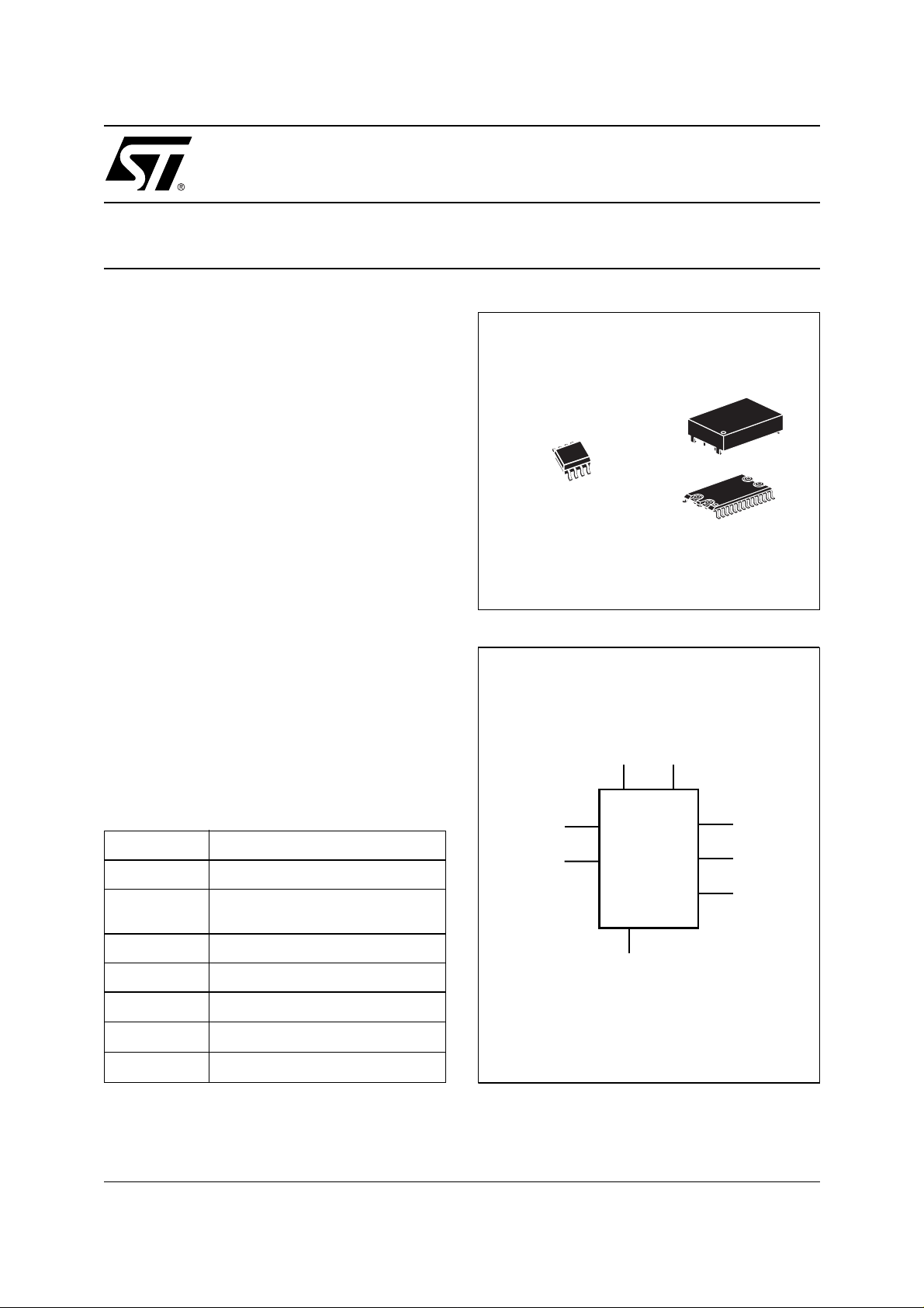
■ PACKAGING INCLUDES a 28-LEAD SOIC and
SNAPHAT
®
TOP (to be Ordered Separately)
8
1
SO8 (M)
150mil Width
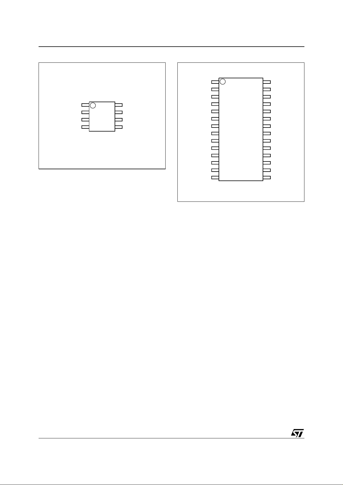
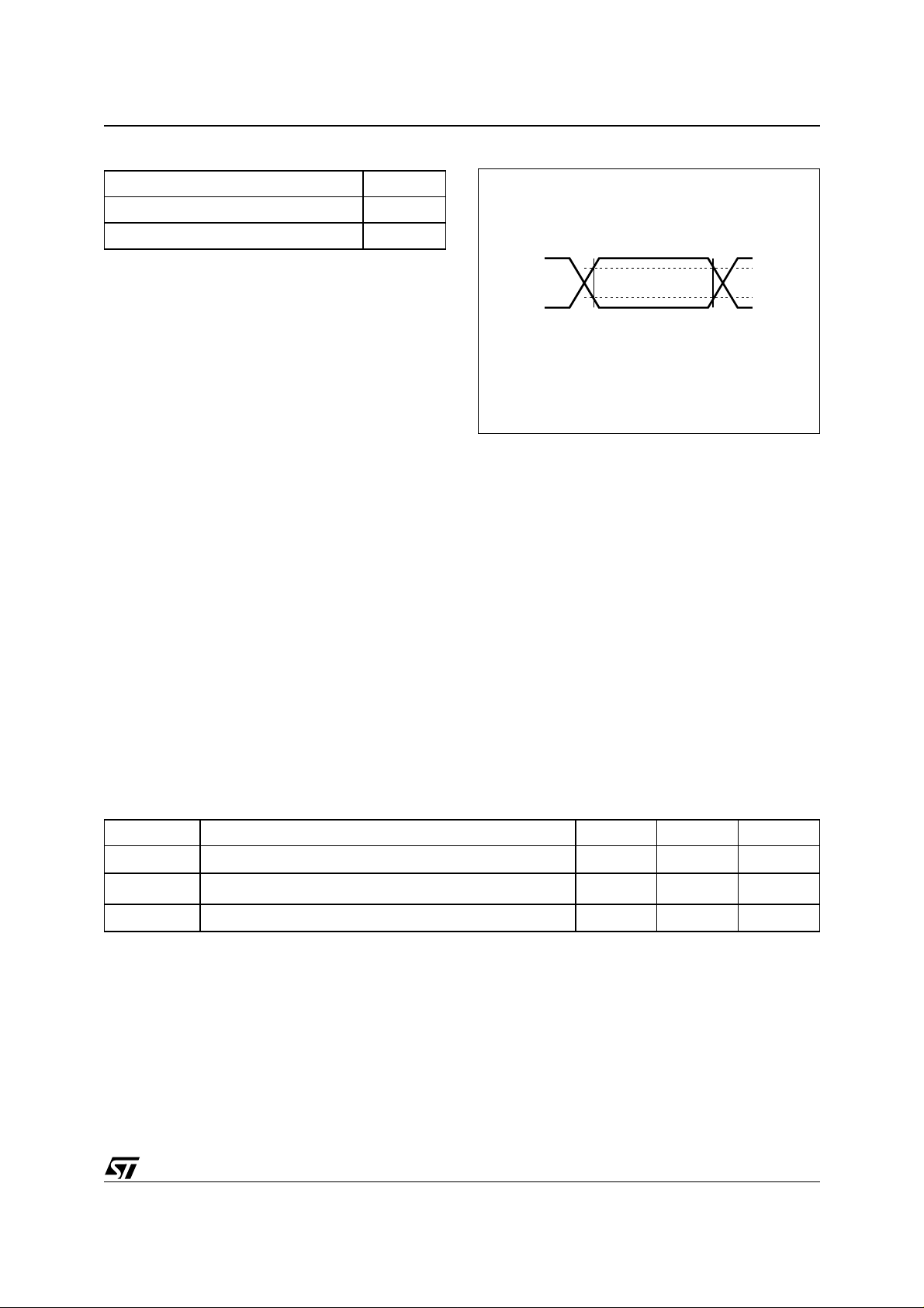
Figure 1. Logic Diagram
M41T56
SNAPHAT (SH)
Battery & Crystal
28
1
SOH28 (MH)
Table 1. Signal Names
OSCI Oscillator Input
OCSO Oscillator Output
FT/OUT
SDA Serial Data Address Input / Output
SCL Serial Clock
V
BAT
V
CC
V
SS
Frequency Test / Output Driver
(Open Drain)
Battery Supply Voltage
Supply Voltage
Ground
OSCI
SCL
V
CC
M41T56
V
SS
V
BAT
OSCO
SDA
FT/OUT
AI02304B
1/19March 2000
M41T56
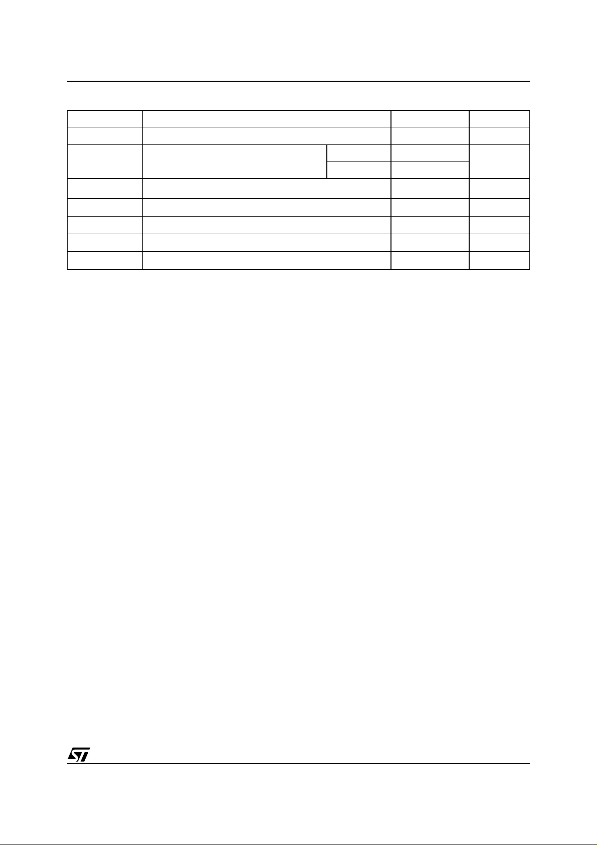
Figure 2A. SO8 Pin Connections
M41T56
OSCI V
V
BAT
SS
1
2
3
4
8
7
6
5
AI02306B
CC
FT/OUTOSCO
SCL
SDAV
DESCRIPTION
®
The M41T56 TIMEKEEPER
is a low power 512
bit static CMOS RAM organized as 64 words by 8
bits. A built-in 32.768 kHz oscillator (external cry stal controlled) and the first 8 bytes of the RAM are
used for the clock/calendar function and are configured in binary coded decimal (BCD) format. Addresses and data are transferred serially via a twoline bi-directional bus. The built-in address register
is incremented automatically after each write or
read data byte.
The M41T56 clock has a built-in power sense circuit which detects power failures and automatically switches to the battery supply during power
failures. The energy needed to sustain the RAM
and clock operations can be supplied from a small
lithium co in cell.
Typical data retention time is in excess of 10years
with a 50mAh 3V lithium cell. The M41T56 is supplied in 8 lead Plastic SOIC package or 2 8 lead
SNAPHAT package.
The 28 pin 330mil SOIC provides sockets with
gold plated contacts at both ends for direct con-
Figure 2B. SOH28 Connections
NC V
NC
NC
NC
NC
NC
NC
NC
NC
NC
NC
NC
NC
V
SS
1
2
3
4
5
6
7
8
9
10
11
12
13
14
M41T56
28
27
26
25
24
23
22
21
20
19
18
17
16
15
AI03607
CC
NC
FT/OUT
NC
NC
NC
NC
NC
SCL
NC
NC
NC
SDA
NC
nection to a separate SNAPHAT housing cont aining the battery and crystal. The unique design
allows the SNAPHAT battery package to be
mounted on top of the SOIC package after the
completion of the surface mount process. Insertion of the SNAPHAT housing after reflow prevents potential battery and c rystal dam age due to
the high temperatures required for device surfacemounting. The SNAPHAT housing is keyed to prevent reverse insertion. The SOIC and battery/crystal packages are shipped separately in plastic antistatic tubes or in Tape & Reel form.
For the 28 lead SOIC, the battery/crystal package
(i.e. SNAPHAT) part number is "M4TxxBR12SHx".
Caution: Do not place the SNAPHAT battery/crystal package "M4Txx-BR12SHx" in conductive
foam since this will drain the lithium button-cell
battery.
2/19
M41T56
Table 2. Absolute Maximum Ratings
Symbol Parameter Value Unit
T
A
T
STG
(2)
T
SLD
V
IO
V
CC
I
O
P
D
Note: 1. Stresses greater than those listed under "Absolute Maximum Ratings" may cause permanent damage to the device. This is a stress
rating only and function al operation of th e device at thes e or any other conditions above those indic at ed in the operational section
of this spec ification is not im plied. Exposure t o the abso lute max imum rat ing cond itions for extende d period s of tim e may affe ct
reliability.
2. Soldering temperature not to exceed 260°C for 10 seconds (total thermal budget not to exceed 150°C for longer than 30 seconds).
CAUTION: Negative undershoo ts bel ow –0.3V are not al l owed on any pin whil e i n the Battery Back-up mode.
CAUTION: Do NOT wave solder SOIC to avoid damaging SNAPHAT sockets.
Ambient Operating Temperature –40 to 85 °C
Storage Temperature (VCC Off, Oscillator Off)
Lead Solder Temperature for 10 seconds 260 °C
Input or Output Voltages –0.3 to 7 V
Supply Voltage –0.3 to 7 V
Output Current 20 mA
Power Dissipation 0.25 W
OPERATION
The M41T56 clock operates as a slave device on
the serial bus. Access is obtained by implementing
a start condition followed by the correct slave address (D0h). The 64 bytes contained in the device
can then be accessed sequentially in the following
order:
1. Seconds Register
2. Minutes Register
3. Century/Hours Register
4. Day Register
5. Date Register
(1)
SNAPHAT –40 to 85
SOIC –55 to 125
The clock continually monitors V
tolerance condition. Should V
CC
CC
fall below V
°C
for an out of
PFD
the device terminates a n access in progress and
resets the device address counte r. Inputs to the
device will not be recognized at this time to prevent erroneous data fr om being writt en to the device from an out of tolerance system. W hen V
falls below V
, the device automatically switch-
BAT
CC
es over to the battery and powers down into an ultra low current mode of operation to conserve
battery life. Upon power-up, the device switches
from battery to V
when V
goes above V
CC
CC
at V
and recognizes inputs
BAT
volts.
PFD
6. Month Register
7. Years Register
8. Control Register
9 to 64.RAM
,
3/19
M41T56
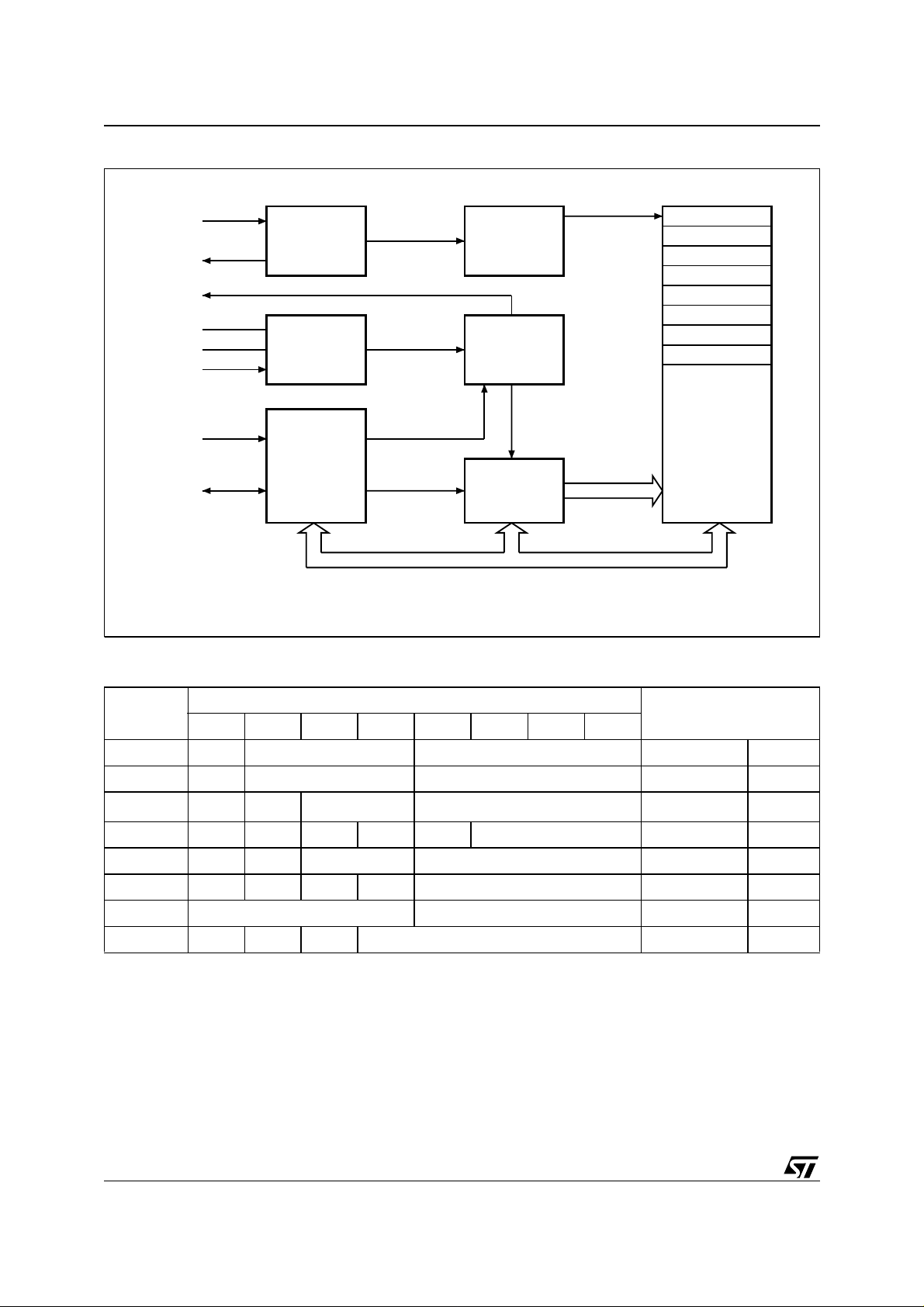
Figure 3. Block Diagram
OSCI
OSCO
FT/OUT
V
CC
V
SS
V
BAT
SCL
SDA
OSCILLATOR
32.768 kHz
VOLTAGE
SENSE
and
SWITCH
CIRCUITRY
SERIAL
BUS
INTERFACE
DIVIDER
CONTROL
LOGIC
ADDRESS
REGISTER
1 Hz
SECONDS
MINUTES
CENTURY/HOURS
DAY
DATE
MONTH
YEAR
CONTROL
RAM
(56 x 8)
AI02566
Table 3. Register Map
Address
Data
D7 D6 D5 D4 D3 D2 D1 D0
0 ST 10 Seconds Seconds Seconds 00-59
1 X 10 Minutes Minutes Minutes 00-59
(1)
2
CEB
CB 10 Hours Hours Century/Hour 0-1/00-23
3 XXXXX Day Day 01-07
4 X X 10 Date Date Date 01-31
5 X X X 10 M. Month Month 01-12
6 10 Years Years Year 00-99
7 OUT FT S Calibration Control
Note: 1. When CEB is set to ’1’, CB will toggle from ’0’ to ’1’ or from ’1’ to ’0’ every 100 years (dependent upon the initial value set).
Keys: S = SIGN Bit;
When CEB is set to ’0’, CB will not toggle.
FT = FREQUENCY TEST Bit;
ST = STOP Bit;
OUT = Output level;
X = Don’t care;
CEB = Century Enable Bit;
CB = Centur y B i t.
Function/Ran ge
BCD Format
4/19
M41T56
Table 4. AC Measurement Conditions
Input Rise and Fall Times ≤ 5ns
Input Pulse Voltages 0 to 3V
Input and Output Timing Ref. Voltages 1.5V
Note that Output Hi-Z is defined as the point where data is no longer
driven.
2-WIRE BUS CHARACTERISTICS
This bus is intended for communication between
different ICs. It consists of two lines: one bi-directional for data signals (SDA) and one for clock signals (SCL). Both the SDA and the SCL lines must
be connected to a positive supply voltage via a
pull-up resistor.
The following protocol has been defined:
– Data transfer may be initiated only when the bus
is not busy.
– During data trans fer, the dat a line mus t remain
stable whenever the clock line is High.
– Changes in the dat a line while the clock line is
High will be interpreted as control signals.
Accordingly, the following bus conditions have
been defined:
Bus not busy. Both data and clock lines remain
High.
Start data transfer. A change in the state of t he
data line, from High to Low, while the clock is High,
defines the START condition.
Stop data transfer. A change in the state of the
data line, from Low to High, while the clock is High,
defines the STOP condition.
Figure 4. AC Testing Load Circuit
0.8V
0.2V
CC
CC
0.7V
0.3V
AI02568
CC
CC
Data valid. The state of the data line represents
valid data when after a start condition, the data line
is stable for the duration of the High period of the
clock signal. The data on the line may be changed
during the Low period of the clock signal. There is
one clock pulse per bit of data.
Each data transfer is initiated with a start condition
and terminated with a stop condition. The number
of data bytes transferred between the start and
stop conditions is not limited. The information is
transmitted byte-wide and each receiver acknowledges with a ninth bit.
By definition, a device that gives out a message is
called "transmitter", the receiving de vice t hat g ets
the message is called "rece iver". The device that
controls the message is called "master". The devices that are controlled by the master are cal led
"sla ve s".
Table 5. Capacitance
(T
= 25 °C, f = MHz)
A
Symbol Parameter Min Ma x Unit
C
IN
C
OUT
t
LP
Note: 1. Effectiv e capacitan ce measured with power supply at 5V.
2. Sampled, not 100% tested.
3. Outputs deselect ed.
Input Capacitance (SCL) 7 pF
(3)
Output Capacitance (SDA, FT/OUT) 10 pF
Low-pass filter input time constant (SDA and SCL) 0.25 1 µs
(1, 2)
5/19
M41T56
Table 6. DC Characteristics
(T
= –40 to 85 °C; VCC = 4.5V to 5.5V)
A
Symbol Parameter Test Condition Min Typ Max Unit
I
I
I
CC1
I
CC2
V
V
V
V
BA T
I
BA T
Note: 1. STMicro el ectronics recommend s t he RAYOVAC BR 1225 or BR1632 (or equivalent) as the battery supply.
Input Leakage Current
LI
Output Leakage Current
LO
Supply Current Switch Frequency = 100kHz 300 µA
Supply Current (Standby)
Input Low Voltage –0.3
IL
Input High Voltage
IH
Output Low Voltage
OL
(1)
Battery Supply Voltage 2.5 3 3.5 V
Battery Supply Current
0V ≤ V
0V ≤ V
SCL, SDA = V
I
= 5mA, VCC = 4.5V
OL
T
= 25°C, VCC = 0V,
A
Oscillator ON, V
Table 7. Power Down/Up Trip Points DC Characteristics
IN
OUT
≤ V
≤ V
CC
CC
CC
– 0.3V
= 3V
BAT
±1 µA
±1 µA
100 µA
1.5
3V
CC
0.4 V
450 550 nA
(1)
+ 0.8
(TA = –40 to 85 °C)
Symbol Parameter Min Typ Max Unit
V
PFD
V
SO
Note: 1. All voltages referenced to VSS.
Power-fail Deselect Voltage
Battery Back-up Switchover Voltage
1.2 V
BA T
1.25 V
V
BAT
BA T
1.285 V
BA T
V
V
V
V
Table 8. Crystal Electrical Characteristics
(Externally Supplied if using the SO8 package)
Symbol Parameter Min Typ Max Unit
f
O
R
S
C
L
Note: L oad cap acitors are inte grated w ithin the M 41T56 . Circuit b oard lay out consi deration s for the 32.768 kH z crysta l of minimu m trace
lengths and isolation from RF generating signals should be taken into account .
STMicroelectron i cs recommends the KDS DT-38 Tuning Fork Type quartz crystal for industrial temperature op erat i ons.
KDS can b e contacted at 9 13-491-6825 or http://w ww.kd sj.co.jp for furt her information on this crystal type.
All SNAP HA T battery/cry st al tops meet thes e specifications.
Resonant Frequency 32.768 kHz
Series Resistance 35 kΩ
Load Capacitance 12.5 pF
6/19

Table 9. Power Down/Up AC Characteristics
(T
= –40 to 85 °C)
A
Symbol Parameter Min Max U nit
M41T56
t
PD
t
FB
t
RB
t
REC
SCL and SDA at VIH before Power Down
V
(min) to VSS VCC Fall Time
PFD
VSS to V
SCL and SDA at VIH after Power Up
(min) VCC Rise Time
PFD
Figure 5. Power Down/Up Mode AC Waveforms
V
CC
V
PFD
VSO
SDA
SCL
I
BAT
tPD
tFB
DATA RETENTION TIME
0ns
300 µs
100 µs
10 µs
tRB
tREC
AI00595
Acknowledge. Each byte of eight bits is followed
by one acknowledge bit. This acknowledge bit is a
low level put on the bus b y the receiver, whereas
the master generates an extra acknowledge related clock pulse.
A slave receiver which is addressed is obliged to
generate an acknowledge after the reception of
each byte. Also, a master receiver must generate
an acknowledge a fter the reception of e ach byte
that has been clocked out of the slave transmitter.
The device that acknowledges has to pull down
the SDA line during the acknowledge clock pulse
in such a way that the SDA line is a stable Low during the High period of the acknowledge related
clock pulse. Of course, setup and hold times must
be taken into account. A master receiver must signal an end-of-data to the slave transm itter by not
generating an acknowledge on t he last byte that
has been clocked out of the slave. In this case, the
transmitter must leave the data line High to enable
the master to generate the STOP condition.
7/19

M41T56
Table 10. AC Characteristics
(T
= –40 to 85 °C; VCC = 4.5V to 5.5V)
A
Symbol Parameter Min Max Unit
f
SCL
t
LOW
t
HIGH
t
R
t
t
HD:STA
t
SU:STA
t
SU:DA T
t
HD:DAT
t
SU:STO
t
BUF
Note: 1. Transmitter must internally provide a hold time to bridge the undefined region (300ns max.) of the falling edge of SCL.
WRITE MODE
In this mode the master transmitter transmits to
the M41T56 slave receiver. Bus protocol is shown
in Figure 10. Following the START condition and
slave address, a logic ’0’ (R/W
bus and indicates to the addressed device that
word address An will follow and is to be written to
the on-chip address p ointer. Th e data wo rd to be
written to the memory is strobed in next and the internal address pointer is incremented to the next
memory location within the RAM on the reception
of an acknowledge clock. The M 41T56 slave receiver will send an acknowledge clock to the master transmitter after it has received the slave
address and again after it has received the word
address and each data byte (see Figure 9).
READ MODE
In this mode, the master reads the M41T56 s lave
after setting the slave address (see Figure 11).
Following the write mode control bit (R/W
the acknowledge bit, the word address A
SCL Clock Frequency 0 100 kHz
Clock Low Period 4.7 µs
Clock High Period 4 µs
SDA and SCL Rise Time 1 µs
SDA and SCL Fall Time 300 ns
F
START Condition Hold Time
(after this period the first clock pulse is generated)
START Condition Setup Time
(only relevant for a repeated start condition)
Data Setup Time 250 ns
(1)
Data Hold Time 0 µs
STOP Condition Setup Time 4.7 µs
Time the bus must be free before a new transmission can start 4.7 µs
4µs
4.7 µs
ten to the on-chip address pointer. Next the
START condition and slave address are repeated,
followed by the READ mode control bit (R/W
At this point, the master transmitter becomes the
= 0) is placed on the
master receiver. The data byte which was addressed will be transmitted and the master receiver will send an acknowledge bit to the slave
transmitter. The address pointer is only incremented on reception of an acknowledge bit. The
M41T56 s lave tr ansmitt er will now place the data
byte at address A
+ 1 on the bus. The master re-
n
ceiver reads and acknowledges the n ew byte and
the address pointer is incremented to A
This cycle of reading con secutive addresses will
continue until the mast er receiver sends a STOP
condition to the slave transmitter.
An alternate READ mode may also be implemented, whereby the master reads the M41T56 slave
without first writing to the (volatile) a ddress pointer. The first address that is read is the last one
= 0) and
is writ-
n
stored in the pointer, see Figure 12.
n
= 1).
+ 2.
8/19

Figure 6. Serial Bus Data Transfer Sequence
DATA LINE
STABLE
DATA VALID
CLOCK
DATA
M41T56
START
CONDITION
Figure 7. Acknowledgment Sequen ce
START
SCLK FROM
MASTER
DATA OUTPUT
BY TRANSMITTER
DATA OUTPUT
BY RECEIVER
12 89
MSB LSB
CLOCK OPERATION
The eight byte clock register (see Table 3) is used
to both set the clock and to read the date and time
from the clock, in a binary coded decimal form at.
Seconds, Minutes, and Hours are contained within
the first three registers. Bits D6 and D7 of clock
register 2 (Hours Register) contain the CENTURY
ENABLE Bit (CEB) and the CENTURY Bit (CB).
Setting CEB to a ’1’ will cause CB to toggle, either
from ’0’ to ’1’ or from ’1’ to ’0’ at the turn of the century (depending upon its initial state). If CEB is set
to a ’0’, CB will not toggle. Bits D0 through D2 of
register 3 contain the Day (day of week). Registers
4, 5 and 6 contain the Date (day of month), Month
and Years. The final register is the Control Register (this is described in the Clock Calibration section). Bit D7 of register 0 contains the STOP Bit
(ST). Setting this bit to a ’1’ will cause the oscillator
CHANGE OF
DATA ALLOWED
STOP
CONDITION
AI00587
CLOCK PULSE FOR
ACKNOWLEDGEMENT
AI00601
to stop. If the device is expected to spend a significant amount of time on the shelf, the oscillator
may be stopped to reduce current drain. When reset to a ’0’ the oscillator restarts within one second.
The seven Clock Registers may be read one byte
at a time, or in a sequential block. The Control
Register (Address location 7) may be accessed independently. Provision has been made to assure
that a clock update does not occur while any of the
seven clock addresses are being read. If a clock
address is being read, an update of the clock registers will be delayed by 250ms to allow the read
to be completed before the update occurs. This
will prevent a tran s it ion of da t a d ur ing t he re ad .
Note: This 250ms delay affects only the clock register update and does not alter the actual clock
time.
9/19

M41T56
Figure 8. Bus Timing Requirements Sequence
SDA
tHD:STAtBUF
tR
SCL
SP
Note: P = STOP and S = START
tF
tHIGH
tLOW
Figure 9. Slave Address Location
R/W
START A
SLAVE ADDRESS
MSB
0100011
LSB
AI00602
CLOCK CALIBRATION
The M41T56 is driven by a quartz controlled oscillator with a nominal frequency of 32,768Hz. The
devices are tested not to exceed 35ppm (parts per
million) oscillator frequency error at 25°C , which
equates to about ±1.53 m inutes per month. With
the calibration bits properly set, the accuracy of
each M41T56 im proves to better than +1/–2 ppm
at 25°C.
The oscillation rate of any crystal changes with
temperature (see Figure 14). Most clock chips
compensate for crystal frequency and temperature shift error with cumbersome trim capacitors.
The M41T56 design, however, employs periodic
tHD:STA
tSU:DAT
tHD:DAT
SR
tSU:STOtSU:STA
P
AI00589
counter correction. The calibration c ircuit adds or
subtracts counts from the o scillator divider circuit
at the divide by 256 stage, as shown in Figure 13.
The number of times pulses are blanked (subtracted, negative calibration) or split (added, positive
calibration) depends upon the value loaded into
the five bit Calibration byte found in the Control
Register. Adding counts speeds the clock up, subtracting counts slows the clock down.
The Calibration byte occupies the five lower order
bits (D4-D0) in the Control register (Addr 7). This
byte can be set to represent any value between 0
and 31 in binary form. Bit D5 is a Sign bit; '1' indicates positive calibration, '0' indicates negative
calibration. Calibration occurs within a 64 m inute
cycle. The first 62 m inutes i n t he c ycle m ay , onc e
per minute, have one second either shortened by
128 or lengthened by 256 oscillator cycles. If a binary '1' is loaded into the register, only the first 2
minutes in the 64 minutes cycle will be modified; if
a binary 6 is loaded, t he first 12 will be affected,
and so on.
Therefore, each cal ibration step has the effect of
adding 512 or subtracting 256 oscillator cycles for
every 125,829,120 actual oscillator cycles, that is
+4.068 or –2.034 ppm of adjustment per calibration step in the cal ibration registe r. Ass um ing that
the oscillator is in fact running at exactly 32,768Hz,
each of the 31 in crements in the Calibration b yte
would represent +10.7 or –5.35 seconds per
month which corresponds to a total range of +5.5
or –2.75 minutes per month.
10/19

Figure 10. Wri t e Mode Sequence
M41T56
BUS ACTIVITY:
MASTER
BUS ACTIVITY:
START
S
SLAVE
ADDRESS
Figure 11. Read Mode Sequence
BUS ACTIVITY:
MASTER
SDA LINE
BUS ACTIVITY:
START
S
SLAVE
ADDRESS
R/W
WORD
ADDRESS (n)
ACK
R/W
WORD
ADDRESS (n)
ACK
DATA n DATA n+1 DATA n+X
ACK
START
S
ACK
SLAVE
ADDRESS
ACK
R/W
DATA n DATA n+1
ACK
ACK
ACK
STOP
PSDA LINE
ACK
AI00591
ACK
DATA n+X
Figure 12. Alternate Read Mode Sequence
BUS ACTIVITY:
MASTER
BUS ACTIVITY:
START
S
SLAVE
ADDRESS
R/W
DATA n DATA n+1 DATA n+X
ACK
STOP
P
NO ACK
ACK
ACK
AI00899
STOP
PSDA LINE
ACK
NO ACK
AI00895
11/19

M41T56
Figure 13. Cloc k C al ib rat i on
NORMAL
POSITIVE
CALIBRATION
NEGATIVE
CALIBRATION
AI00594B
Two methods are available for ascertaining how
much calibration a given M41T56 may require.
The first involves simply setting the clock, letting it
run for a month and comparing it to a known accurate reference (like WWV broadcasts). While that
may seem crude, it allows the designer to give the
end user the ability to calibrate his clock as his environment may require, even after the final product
is packaged in a non-user serviceable enclosure.
All the designer has to do is provide a simple utility
that accessed the Calibration byte.
The second approach is better suit ed to a manufacturing environment, and involves the use of
some test equipment. When the F requency Test
(FT) bit, the seventh-most significant bit in the
Control Register, is set to a '1', and the oscillator is
running at 32,768Hz, the FT/OUT pin of the device
will toggle at 512Hz. Any deviation from 512Hz indicates t he degre e and direc tion of o scillator frequency shift at the test temperature.
For example, a reading of 512.01024Hz woul d indicate a +20ppm oscillator frequency error, requir-
ing a –10(XX001010) to be loaded into the
Calibration Byte for correction. Note that setting or
changing the Calibration Byte does n ot affect the
Frequency test output frequency.
OUTPUT DRIVER PIN
When the FT bit is not set, the FT/OUT pin becomes an output driver that reflects the contents of
D7 of the control register. In other words, when D6
of location 7 is a zero and D7 of location 7 i s a zero
and then the FT/OUT pin will be driven low.
Note: The FT/OUT pin is open drain which requires an external pull-up resistor.
POWER-ON DEFAULTS
Upon initial application of power to the device, the
FT bit will be set to a '0' and the OUT bit will be set
to a '1'. All other Register bits will initially power-on
in a random state.
12/19

Figure 14. Crystal Accuracy Across Temp eratur e
Frequency (ppm)
20
0
–20
–40
–60
–80
∆F
–100
–120
–140
–160
0 10203040506070
Temperature °C
= -0.038 (T - T
F
ppm
C
T0 = 25 °C
M41T56
)2 ± 10%
0
2
80–10–20–30–40
AI00999
13/19

M41T56
Table 11. Ordering Information Scheme
Example: M41T56 M 6 TR
Device Type
M41T
Package
M = SO8 150mils width
MH = SOH28
Temperature Range
6 = –40 to 85 °C
Shipping Method for SO
blank = Tubes
TR = Tape & Reel
Note: T he SOIC package (SOH28) requires the batt ery package (S NAPHAT) whi ch is ordered separately un der the part number
"M4Txx-BR12SHx " in pl astic tube or "M 4T xx-BR12SHxTR" in Tape & Reel form.
Cautio n: Do not place the SNAPHAT battery package "M4Txx-BR12SHx" in conductive foam since thi s will drain the lit hium butt on-cell battery.
For a list of available options or for further inform ation on any aspect of this device, please contact the
STMicroelectronics Sales Office near e st to you.
Table 12. Revision History
Date Revision Details
March 1999 F irst Issue
12/23/99 SOH28 package added
03/21/00 Series Resistance Max Value Changed (Table 8)
14/19

M41T56
Table 13. SO8 - 8 pin Plastic Small Outline, 150 mils body width, Packag e Mechani cal Data
Symb
Typ Min Max Typ Min Max
A 1.35 1.75 0.053 0.069
A1 0.10 0.25 0.004 0.010
B 0.33 0.51 0.013 0.020
C 0.19 0.25 0.007 0.010
D 4.80 5.00 0.189 0.197
E 3.80 4.00 0.150 0.157
e 1.27 – – 0.050 – –
H 5.80 6.20 0.228 0.244
h 0.25 0.50 0.010 0.020
L 0.40 0.90 0.016 0.035
α 0° 8° 0° 8°
N8 8
CP 0.10 0.004
mm inches
Figure 15. SO8 - 8 pin Plastic Small Outline, 150 mils body width, Package Outline
h x 45˚
A
C
B
e
CP
D
N
E
H
1
LA1 α
SO-a
Drawing is not to scale.
15/19

M41T56
Table 14. SOH28 - 28 lead Plastic Small Outline, 4-socket battery SNAPHAT,
Package Mechanical Data
Symb
Typ Min Max Typ Min Max
A 3.05 0.120
A1 0.05 0.36 0.002 0.014
A2 2.34 2.69 0.092 0.106
B 0.36 0.51 0.014 0.020
C 0.15 0.32 0.006 0.012
D 17.71 18.49 0.697 0.728
E 8.23 8.89 0.324 0.350
e 1.27 – – 0.050 – –
eB 3.20 3.61 0.126 0.142
H 11.51 12.70 0.453 0.500
L 0.41 1.27 0.016 0.050
α 0° 8° 0° 8°
N 28 28
CP 0.10 0.004
mm inches
Figure 16. SOH28 - 28 lead Plastic Small Outline, 4-socket battery SNAPHAT, Package Outline
A2
A
C
Be
eB
CP
D
N
E
H
LA1 α
1
SOH-A
Drawing is not to scale.
16/19

M41T56
Table 15. SH - 4-pin SNAPHAT Housing for 48 mAh Battery & Crystal, Package Mechanical Data
Symb
Typ Min Max Typ Min Max
A 9.78 0.385
A1 6.73 7.24 0.265 0.285
A2 6.48 6.99 0.255 0.275
A3 0.38 0.015
B 0.46 0.56 0.018 0.022
D 21.21 21.84 0.835 0.860
E 14.22 14.99 0.560 0.590
eB 3.20 3.61 0.126 0.142
L 2.03 2.29 0.080 0.090
mm inches
Figure 17. SH - 4-pin SNAPHAT Housing for 48 mAh Battery & Crystal, Package Outline
A1
eA
D
A
B
eB
A3
L
E
SHTK-A
Drawing is not to scale.
A2
17/19

M41T56
Table 16. SH - 4-pin SNAPHAT Housing for 120 mAh Battery & Crystal, Package Mechanical Data
Symb
Typ Min Max Typ Min Max
A 10.54 0.415
A1 8.00 8.51 0.315 0.335
A2 7.24 8.00 0.285 0.315
A3 0.38 0.015
B 0.46 0.56 0.018 0.022
D 21.21 21.84 0.835 0.860
E 17.27 18.03 0.680 0.710
eB 3.20 3.61 0.126 0.142
L 2.03 2.29 0.080 0.090
mm inches
Figure 18. SH - 4-pin SNAPHAT Housing for 120 mAh Battery & Crystal, Package Outline
A1
eA
D
A
B
eB
A3
L
E
SHTK-B
Drawing is not to scale.
A2
18/19

M41T56
Information furnishe d is bel i eved to be accurate and reliable. However, STMicroelectroni cs assumes no responsibility for t he consequences
of use of such information nor for any infringement of patents or other rights of third parties which may result from its use. No license is granted
by implic ation or oth erwise unde r any patent or patent rights of STMi croelectronics. Speci fications me ntioned in th i s publication are subject
to change without notice. This publication supersedes and replaces all information previously supplied. STMicroelectronics products are not
authorized for use as crit i cal component s i n l i f e support devices or systems wi thout expre ss written appr oval of STMicroelectronics.
The ST log o i s registered trademark of STM i croelectronics
2000 STMicroel e ctronics - All Ri ghts Reserved
All other names are the property of their respectiv e owners.
Australi a - Brazil - China - Finland - France - Germany - Hong Kong - India - Italy - Japan - Malaysia - Malta - Moroc co -
Singapor e - Spain - Sweden - Switzerla nd - United Kingdom - U.S.A.
STMicroelect ro n ics GRO UP OF COMPANI ES
http://www.st.com
19/19
 Loading...