

512 bit (64b x8) Serial Access TIMEKEEPER® SRAM
■ 2.0V to 5.5V SUPPLY VOLTAGE
■ COUNTERS for SECONDS, MINUTES,
HOURS, DAY, DATE , MONTH, YEARS and
CENTURY
■ YEAR 2000 COMPLIANT
■ SOFTWARE CLOCK CALIBRATION
■ AUTOMATIC SWITCH-OVER and DESELECT
CIRCUITRY
2
■ I
C BUS C O MPATI BLE
■ 56 BYTES of GENERAL PURPOSE RAM
■ ULTRA-LOW BATTER Y SU PPL Y CU RRE N T
of 1µA
■ LOW OPERATING CURRENT of 300µA
■ OPERATING TEMP ERATURE of –40 to 85°C
■ AUTOMATIC LEAP YEAR COMPENSATION
■ SPECIAL SOFTWARE PROGRAMMABLE
OUTPUT
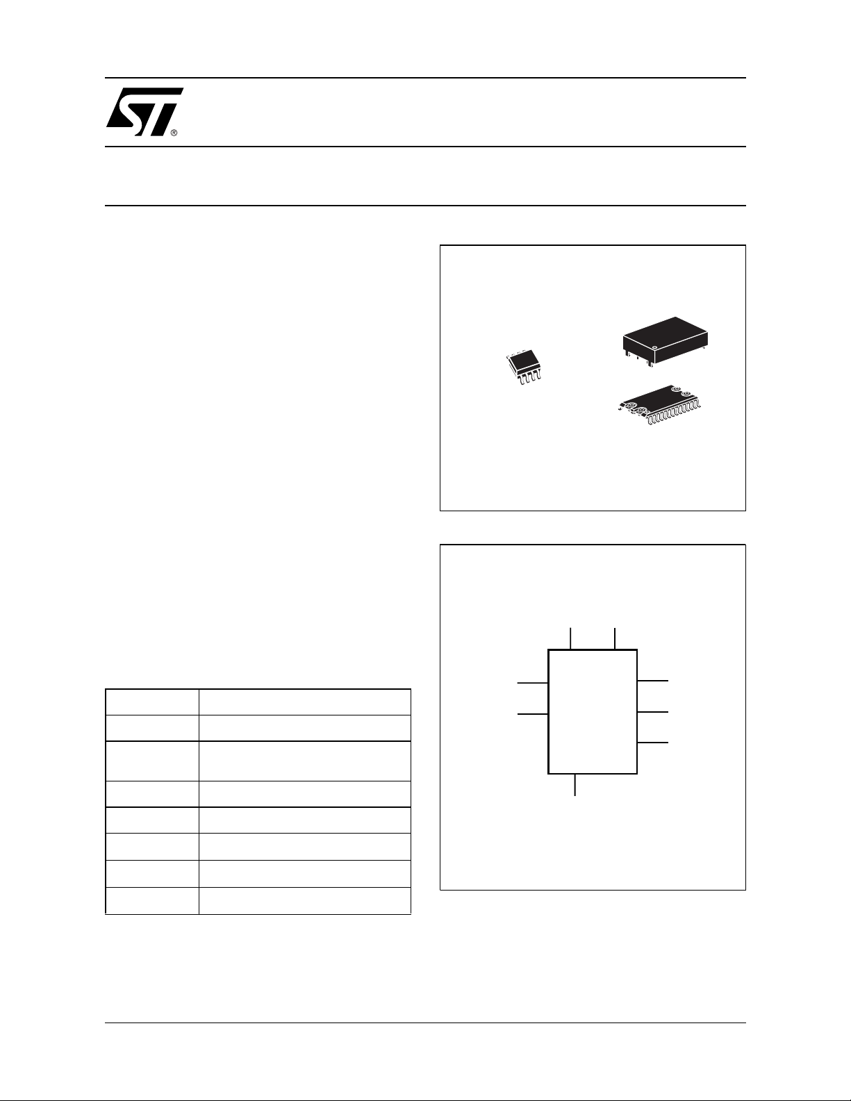
■ PACKAGING INCLUDES a 28-LEAD SOIC and
SNAPHAT
®
TOP (to be Ordered Separately)
8
1
SO8 (M)
150mil Width
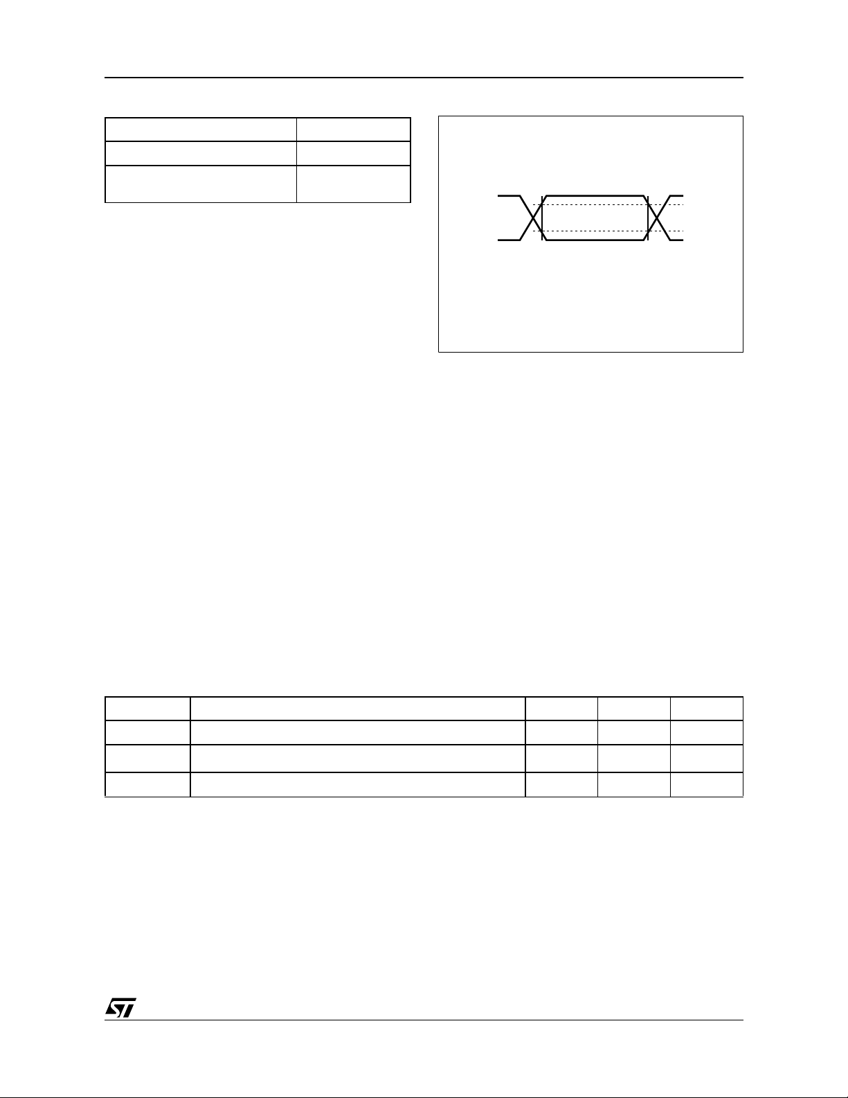
Figure 1. Logic Diagram
V
CC
M41T11
SNAPHAT (SH)
Battery & Crystal
28
1
SOH28 (MH)
V
BAT
Table 1. Signal Names
OSCI Oscillator Input
OCSO Oscillator Output
FT/OUT
SDA Serial Data Address Input / Output
SCL Serial Clock
V
BAT
V
CC
V
SS
Frequency Test / Output Driver
(Open drain)
Battery Supply Voltage
Supply Voltage
Ground
OSCI
SCL
M41T11
V
SS
OSCO
SDA
FT/OUT
AI01000
1/19May 2000
M41T11
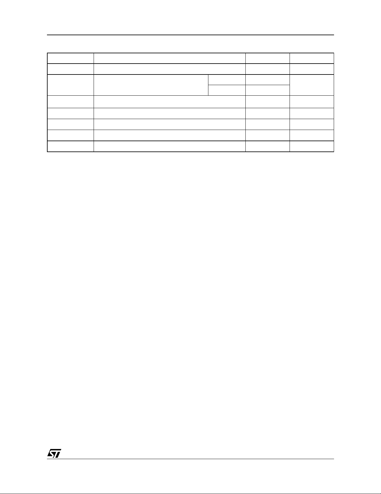
Figure 2A. SO8 Connections
M41T11
OSCI V
V
BAT
SS
1
2
3
4
8
7
6
5
AI01001
CC
FT/OUTOSCO
SCL
SDAV
DESCRIPTION
®
The M41 T1 1 TIMEKEEPER
RAM is a low power
512 bit static CMOS RAM organized as 64 words
by 8 bits. A built-in 32. 768 k Hz osc illat or (e xte rna l
crystal controlled) and the first 8 bytes of the RAM
are used for the c lock/calendar function and are
configured in binary coded decimal (BCD) form at.
Addresses and data are transferred serially via a
two-line bi-directional bus. The built-in address
register is incremented automatically after each
write or read data byte.
The M41T11 clock has a built-in power sense circuit which detects power failures and automatically switches to the battery supply during power
failures. The energy needed to sustain the RAM
and clock operations can be supplied from a small
lithium co in cell.
Typical data retention time is i n ex ces s of 5 years
with a 50mA/h 3V lithium cell. The M41T11 is supplied in 8 lead Plastic Small Outline package or 28
lead SNAPHAT package.
The 28 pin 330mil SOIC provides sockets with
gold plated contacts at both ends for direct connection to a separate SNAPHAT housing cont ain-
Figure 2B. SOH28 Connections
NC V
NC
NC
NC
NC
NC
NC
NC
NC
NC
NC
NC
NC
V
SS
1
2
3
4
5
6
7
8
9
10
11
12
13
14
M41T11
28
27
26
25
24
23
22
21
20
19
18
17
16
15
AI03606
CC
NC
FT/OUT
NC
NC
NC
NC
NC
SCL
NC
NC
NC
SDA
NC
ing the battery and crystal. The unique design
allows the SNAPHAT battery package to be
mounted on top of the SOIC package after the
completion of the surface mount process. Insertion of the SNAPHAT housing after reflow prevents potential battery and c rystal dam age due to
the high temperatures required for device surfacemounting. The SNAPHAT housing is keyed to prevent reverse insertion. The SOIC and battery/crystal packages are shipped separately in plastic antistatic tubes or in Tape & Reel form.
For the 28 lead SOIC, the battery/crystal package
(i.e. SNAPHAT) part number is "M4TxxBR12SHx".
Caution: Do not place the SNAPHAT battery/crystal package "M4Txx-BR12SHx" in conductive
foam since this will drain the lithium button-cell
battery.
2/19
M41T11
Table 2. Absolute Maximum Ratings
Symbol Parameter Value Unit
T
A
T
STG
(2)
T
SLD
V
IO
V
CC
I
O
P
D
Note: 1. Stresses greater than those listed under "Absolute Maximum Ratings" may cause permanent damage to the device. This is a stress
rating only and function al operation of th e device at thes e or any other conditions above those indic at ed in the operational section
of this spec ification is not im plied. Exposure t o the abso lute max imum rat ing cond itions for extende d period s of tim e may affe ct
reliability.
2. Soldering temperature not to exceed 260°C for 10 seconds (total thermal budget not to exceed 150°C for longer than 30 seconds).
CAUTION: Negative undershoo ts bel ow –0.3V are not al l owed on any pin whil e i n the Battery Back-up mode.
CAUTION: Do NOT wave solder SOIC to avoid damaging SNAPHAT sockets.
Ambient Operating Temperature –40 to 85 °C
Storage Temperature (VCC Off, Oscillator Off)
Lead Solder Temperature for 10 seconds 260 °C
Input or Output Voltages –0.3 to 7 V
Supply Voltage –0.3 to 7 V
Output Current 20 mA
Power Dissipation 0.25 W
OPERATION
The M41T11 clock operates as a slave device on
the serial bus. Access is obtained by implementing
a start condition followed by the correct slave address (D0h). The 64 bytes contained in the device
can then be accessed sequentially in the following
order:
1. Seconds Register
2. Minutes Register
3. Century/Hours Register
4. Day Register
(1)
SNAPHAT –40 to 85
SOIC –55 to 125
The M41T11 clock continually monitors V
out of tolerance condition. Shoul d V
V
, the device terminates an ac ces s in progress
SO
°C
CC
fall belo w
CC
for an
and resets the device ad dress counter. Inputs to
the device will not be recognized at this time to
prevent erroneous data from being written to the
device from an out of tolerance system. When V
CC
falls below VSO, the device automatically switches
over to the battery and powers down into an ult ra
low current mode of operation to conserve battery
life. Upon power-up, the device switches from battery to V
at VSO and recognizes inputs.
CC
5. Date Register
6. Month Register
7. Years Register
8. Control Register
9 to 64.RAM
3/19
M41T11
Figure 3. Block Diagram
OSCI
OSCO
FT/OUT
V
CC
V
SS
V
BAT
SCL
SDA
OSCILLATOR
32.768 kHz
VOLTAGE
SENSE
and
SWITCH
CIRCUITRY
SERIAL
BUS
INTERFACE
DIVIDER
CONTROL
LOGIC
ADDRESS
REGISTER
1 Hz
SECONDS
MINUTES
CENTURY/HOURS
DAY
DATE
MONTH
YEAR
CONTROL
RAM
(56 x 8)
AI02566
Table 3. Register Map
Address
Data
D7 D6 D5 D4 D3 D2 D1 D0
0 ST 10 Seconds Seconds Seconds 00-59
1 X 10 Minutes Minutes Minutes 00-59
(1)
2
CEB
CB 10 Hours Hours Century/Hour 0-1/00-23
3 XXXXX Day Day 01-07
4 X X 10 Date Date Date 01-31
5 X X X 10 M. Month Month 01-12
6 10 Years Years Year 00-99
7 OUT FT S Calibration Control
Note: 1. When CEB is set to ’1’, CB will toggle from ’0’ to ’1’ or from ’1’ to ’0’ every 100 years (dependent upon the initial value set).
Keys: S = SIGN Bit;
When CEB is set to ’0’, CB will not toggle.
FT = FREQUENCY TEST Bit;
ST = STOP Bit;
OUT = Output level;
X = Don’t care;
CEB = Century Enable Bit;
CB = Centur y B i t.
Function/Ran ge
BCD Format
4/19
M41T11
Table 4. AC Measurement Conditions
Input Rise and Fall Times
Input Pulse Voltages
Input and Output Timing Ref.
Voltages
Note that Output Hi-Z is defined as the point where data is no longer
driven.
5ns
≤
0.2V
0.3V
to 0.8V
CC
to 0.7V
CC
CC
CC
2-WIRE BUS CHARACTERISTICS
This bus is intended for communication between
different ICs. It consists of two lines: one bi-directional for data signals (SDA) and one for clock signals (SCL). Both the SDA and the SCL lines must
be connected to a positive supply voltage via a
pull-up resistor.
The following protocol has been defined:
– Data transfer may be initiated only when the bus
is not busy.
– During data trans fer, the dat a line mus t remain
stable whenever the clock line is High.
– Changes in the dat a line while the clock line is
High will be interpreted as control signals.
Accordingly, the following bus conditions have
been defined:
Bus not busy. Both data and clock lines remain
High.
Start data transfer. A change in the state of t he
data line, from High to Low, while the clock is High,
defines the START condition.
Stop data transfer. A change in the state of the
data line, from Low to High, while the clock is High,
defines the STOP condition.
Figure 4. AC Testing Load Circuit
0.8V
0.2V
CC
CC
0.7V
0.3V
AI02568
CC
CC
Data valid. The state of the data line represents
valid data when after a start condition, the data line
is stable for the duration of the High period of the
clock signal. The data on the line may be changed
during the Low period of the clock signal. There is
one clock pulse per bit of data.
Each data transfer is initiated with a start condition
and terminated with a stop condition. The number
of data bytes transferred between the start and
stop conditions is not limited. The information is
transmitted byte-wide and each receiver acknowledges with a ninth bit.
By definition, a device that gives out a message is
called "transmitter", the receiving de vice t hat g ets
the message is called "rece iver". The device that
controls the message is called "master". The devices that are controlled by the master are cal led
"sla ve s".
Table 5. Capacitance
(T
= 25 °C, f = MHz)
A
Symbol Parameter Min Max Unit
C
IN
C
OUT
t
LP
Note: 1. Effectiv e capacitan ce measured with power supply at 5V.
2. Sampled, not 100% tested.
3. Outputs deselect ed.
Input Capacitance (SCL) 7 pF
(3)
Output Capacitance (SDA, FT/OUT) 10 pF
Low-pass filter input time constant (SDA and SCL) 250 1000 ns
(1, 2)
5/19
M41T11
Table 6. DC Characteristics
(T
= –40 to 85 °C; VCC = 2.0V to 5.5V)
A
Symbol Parameter Test Condition Min Typ Max Unit
I
I
I
CC1
I
CC2
V
V
V
V
BA T
I
BA T
Note: 1. STMicro el ectronics recommend s t he RAYOVAC BR 1225 or BR1632 (or equivalent) as the battery supply.
Input Leakage Current
LI
Output Leakage Current
LO
Supply Current Switch Frequency = 100kHz 300 µA
Supply Current (Standby)
Input Low Voltage –0.3
IL
Input High Voltage
IH
Output Low Voltage
OL
(1)
Battery Supply Voltage 2 3 3.5 V
Battery Supply Current
0V ≤ V
0V ≤ V
SCL, SDA = V
T
= 25°C, VCC = 0V,
A
Oscillator ON, V
Table 7. Power Down/Up Trip Points DC Characteristics
I
OL
≤ V
IN
≤ V
OUT
CC
= 3mA
CC
CC
– 0.3V
= 3V
BAT
(1)
0.7V
CC
±1 µA
±1 µA
70 µA
0.3V
CC
VCC + 0.8
0.4 V
0.8 1 µA
(TA = –40 to 85 °C)
Symbol Parameter Min Typ Max Unit
(2)
V
SO
Note: 1. All voltages referenced to VSS.
2. Switch-over and deselect point.
Battery Back-up Switchover Voltage
V
–0.70 V
BA T
–0.50 V
BA T
BA T
–0.30
V
V
V
Table 8. Crystal Electrical Characteristics
(Externally Supplied if using the SO8 package)
Symbol Parameter Min Typ Max Unit
f
O
R
S
C
L
Note: L oad cap acitors are inte grated w ithin the M 41T11 . Circuit b oard lay out consi deration s for the 32.768 kH z crysta l of minimu m trace
lengths and isolation from RF generating signals should be taken into account .
STMicroelectron i cs recommends the KDS DT-38 Tuning Fork Type quartz c rystal for industrial temperature op erat i ons.
KDS can b e contacted at 9 13-491-6825 or http://w ww.kd sj.co.jp for furt her information on this crystal type.
All SNAP HA T battery/cry st al tops meet thes e specifications.
Resonant Frequency 32.768 kHz
Series Resistance 35 k
Ω
Load Capacitance 12.5 pF
6/19
 Loading...