

5.0 OR 3.0V, 512 bit (6 4 x 8) SERIAL
FEATURES SUMMARY
■ 5.0 OR 3.0V OPERATING VO LTA G E
■ SERIAL INTERFACE SU PPO R TS I
(400 KHz)
■ NVRAM SUPERVISOR FOR EXTERNAL
LPSRAM
■ OPTIMIZED FOR MINIMAL INTERCONNECT
TO MCU
■ 2.5 TO 5.5V OSCILLATOR OPERATING
VOLTAGE
■ AUTOMATIC SWITCH-OVER and DESELECT
CIRCUITRY
■ CHOICE OF POWER-FAIL DESELECT
VOLTAGES
– M41ST85Y : V
4.20V ≤ V
– M41ST85W: V
2.55V ≤ V
■ 1.25V REFERENCE (for PFI/PFO)
■ COUNTERS FOR TENTHS/HUNDREDTHS
PFD
PFD
= 4.5 to 5.5V;
CC
≤ 4.50V
= 2.7 to 3.6V;
CC
≤ 2.70V
OF SECONDS, SECONDS, MINUTES,
HOURS, DAY, DATE , MONTH, YEAR, and
CENTURY
■ 44 BYTES OF GENERAL PURPOSE RAM
■ PROGRAMMABLE ALARM and INTE RRUPT
FUNCTION (VALID EVEN DURING BATTERY
BACK-UP MODE)
■ WATCHDOG T IME R
■ MICROPROCESSOR POWER-ON RESET
■ BATTERY LOW FLAG
■ POWER-DOWN TIMESTAMP (HT BIT)
■ ULTRA-LOW BATT ERY SU PPL Y C URRE N T
OF 500nA (MAX)
2
C BUS
M41ST85Y
M41ST85W
RTC and NVRAM SUPERVISOR
■ PACKAGING INCLUD ES A 28-LEAD SOIC and
SNAPHAT
■ SOIC SNAPHAT PACKAGE PROVIDES
DIRECT CONNECTION FOR A SNAPHAT
TOP WHICH CONTAINS THE BATTERY and
CRYSTAL
■ SOIC EMBEDDED CR YSTAL P ACKAG E (M X)
OPTION
Figure 1. 28-pi n S O I C Package
Figure 2. 28-pin (300mil) SOIC Package
®
TOP (to be Ordered Separately)
SNAPHAT (SH)
Battery & Crystal
28
1
SOH28 (MH)
EMBEDDED Cryst al
SOX28 (MX)
Rev. 4.0
1/33May 2003

M41ST85Y, M41ST85W
TABLE OF CONTENTS
SUMMARY DESCRIPTION. . . . . . . . . . . . . . . . . . . . . . . . . . . . . . . . . . . . . . . . . . . . . . . . . . . . . . . . . . . 4
Figure 3. Logic Diagram . . . . . . . . . . . . . . . . . . . . . . . . . . . . . . . . . . . . . . . . . . . . . . . . . . . . . . . . . . 5
Table 1. Signal Names . . . . . . . . . . . . . . . . . . . . . . . . . . . . . . . . . . . . . . . . . . . . . . . . . . . . . . . . . . . 5
Figure 4. 28-pin SOIC Connections. . . . . . . . . . . . . . . . . . . . . . . . . . . . . . . . . . . . . . . . . . . . . . . . . . 5
Figure 6. Block Diagram . . . . . . . . . . . . . . . . . . . . . . . . . . . . . . . . . . . . . . . . . . . . . . . . . . . . . . . . . . 6
Figure 7. Hardware Hookup . . . . . . . . . . . . . . . . . . . . . . . . . . . . . . . . . . . . . . . . . . . . . . . . . . . . . . . 7
MAXIMUM RATING. . . . . . . . . . . . . . . . . . . . . . . . . . . . . . . . . . . . . . . . . . . . . . . . . . . . . . . . . . . . . . . . . 7
Table 2. Absolute Maximum Ratings. . . . . . . . . . . . . . . . . . . . . . . . . . . . . . . . . . . . . . . . . . . . . . . . . 7
DC and AC PARAMETERS . . . . . . . . . . . . . . . . . . . . . . . . . . . . . . . . . . . . . . . . . . . . . . . . . . . . . . . . . . 8
Table 3. DC and AC Measurement Conditions . . . . . . . . . . . . . . . . . . . . . . . . . . . . . . . . . . . . . . . . . 8
Figure 8. AC Testing Input/Output Waveforms . . . . . . . . . . . . . . . . . . . . . . . . . . . . . . . . . . . . . . . . . 8
Table 4. Capacitance. . . . . . . . . . . . . . . . . . . . . . . . . . . . . . . . . . . . . . . . . . . . . . . . . . . . . . . . . . . . . 8
Table 5. DC Characteristics. . . . . . . . . . . . . . . . . . . . . . . . . . . . . . . . . . . . . . . . . . . . . . . . . . . . . . . . 9
OPERATING MODES . . . . . . . . . . . . . . . . . . . . . . . . . . . . . . . . . . . . . . . . . . . . . . . . . . . . . . . . . . . . . . 10
2-Wire Bus Characteristics . . . . . . . . . . . . . . . . . . . . . . . . . . . . . . . . . . . . . . . . . . . . . . . . . . . . . . 10
Figure 9. Serial Bus Data Transfer Sequence. . . . . . . . . . . . . . . . . . . . . . . . . . . . . . . . . . . . . . . . .11
Figure 11. WRITE Cycle Timing: RTC & External SRAM Control Signals . . . . . . . . . . . . . . . . . . . 12
Figure 12. Bus Timing Requirements Sequence. . . . . . . . . . . . . . . . . . . . . . . . . . . . . . . . . . . . . . . 12
Table 6. AC Characteristics. . . . . . . . . . . . . . . . . . . . . . . . . . . . . . . . . . . . . . . . . . . . . . . . . . . . . . . 12
READ Mode . . . . . . . . . . . . . . . . . . . . . . . . . . . . . . . . . . . . . . . . . . . . . . . . . . . . . . . . . . . . . . . . . . 13
Figure 13. Slave Address Location . . . . . . . . . . . . . . . . . . . . . . . . . . . . . . . . . . . . . . . . . . . . . . . . . 13
Figure 14. READ Mode Sequence . . . . . . . . . . . . . . . . . . . . . . . . . . . . . . . . . . . . . . . . . . . . . . . . . 13
Figure 15. Alternate READ Mode Sequence. . . . . . . . . . . . . . . . . . . . . . . . . . . . . . . . . . . . . . . . . . 14
WRITE Mode. . . . . . . . . . . . . . . . . . . . . . . . . . . . . . . . . . . . . . . . . . . . . . . . . . . . . . . . . . . . . . . . . . 14
Figure 16. WRITE Mode Sequence . . . . . . . . . . . . . . . . . . . . . . . . . . . . . . . . . . . . . . . . . . . . . . . . . 14
Data Retention Mode. . . . . . . . . . . . . . . . . . . . . . . . . . . . . . . . . . . . . . . . . . . . . . . . . . . . . . . . . . . 15
Figure 17. Power Down/Up Mode AC Waveforms . . . . . . . . . . . . . . . . . . . . . . . . . . . . . . . . . . . . . 16
Table 7. Power Down/Up AC Characteristics . . . . . . . . . . . . . . . . . . . . . . . . . . . . . . . . . . . . . . . . . 16
CLOCK OPERATION . . . . . . . . . . . . . . . . . . . . . . . . . . . . . . . . . . . . . . . . . . . . . . . . . . . . . . . . . . . . . . 17
TIMEKEEPER® Registers. . . . . . . . . . . . . . . . . . . . . . . . . . . . . . . . . . . . . . . . . . . . . . . . . . . . . . . 17
Table 8. TIMEKEEPER® Register Map . . . . . . . . . . . . . . . . . . . . . . . . . . . . . . . . . . . . . . . . . . . . . 18
Calibrating the Clock. . . . . . . . . . . . . . . . . . . . . . . . . . . . . . . . . . . . . . . . . . . . . . . . . . . . . . . . . . . 1 9
Setting Alarm Clock Registers. . . . . . . . . . . . . . . . . . . . . . . . . . . . . . . . . . . . . . . . . . . . . . . . . . . 19
Figure 18. Alarm Interrupt Reset Waveform . . . . . . . . . . . . . . . . . . . . . . . . . . . . . . . . . . . . . . . . . . 20
Table 9. Alarm Repeat Modes. . . . . . . . . . . . . . . . . . . . . . . . . . . . . . . . . . . . . . . . . . . . . . . . . . . . . 20
Figure 19. Back-Up Mode Alarm Waveform . . . . . . . . . . . . . . . . . . . . . . . . . . . . . . . . . . . . . . . . . . 21
2/33

M41ST85Y, M41ST85W
Watchdog Timer . . . . . . . . . . . . . . . . . . . . . . . . . . . . . . . . . . . . . . . . . . . . . . . . . . . . . . . . . . . . . . 21
Square Wave Outp ut . . . . . . . . . . . . . . . . . . . . . . . . . . . . . . . . . . . . . . . . . . . . . . . . . . . . . . . . . . . 22
Table 10. Square Wave Output Frequency . . . . . . . . . . . . . . . . . . . . . . . . . . . . . . . . . . . . . . . . . . . 22
Power-on Reset . . . . . . . . . . . . . . . . . . . . . . . . . . . . . . . . . . . . . . . . . . . . . . . . . . . . . . . . . . . . . . . 23
Reset Inputs (RSTIN1 & RSTIN2) . . . . . . . . . . . . . . . . . . . . . . . . . . . . . . . . . . . . . . . . . . . . . . . . . 23
Figure 20. RSTIN1 & RSTIN2 Timing Waveforms . . . . . . . . . . . . . . . . . . . . . . . . . . . . . . . . . . . . . 23
Table 11. Reset AC Characteristics . . . . . . . . . . . . . . . . . . . . . . . . . . . . . . . . . . . . . . . . . . . . . . . . 2 3
Power-fail INPUT/OUTPUT . . . . . . . . . . . . . . . . . . . . . . . . . . . . . . . . . . . . . . . . . . . . . . . . . . . . . . 24
Century Bit. . . . . . . . . . . . . . . . . . . . . . . . . . . . . . . . . . . . . . . . . . . . . . . . . . . . . . . . . . . . . . . . . . . 24
Output Driver Pin. . . . . . . . . . . . . . . . . . . . . . . . . . . . . . . . . . . . . . . . . . . . . . . . . . . . . . . . . . . . . . 24
Battery Low Warning. . . . . . . . . . . . . . . . . . . . . . . . . . . . . . . . . . . . . . . . . . . . . . . . . . . . . . . . . . . 24
t
Bit . . . . . . . . . . . . . . . . . . . . . . . . . . . . . . . . . . . . . . . . . . . . . . . . . . . . . . . . . . . . . . . . . . . . . . 24
REC
Initial Power-on Defaults. . . . . . . . . . . . . . . . . . . . . . . . . . . . . . . . . . . . . . . . . . . . . . . . . . . . . . . . 24
Table 12. t
Table 13. Default Values. . . . . . . . . . . . . . . . . . . . . . . . . . . . . . . . . . . . . . . . . . . . . . . . . . . . . . . . . 25
Figure 21. Crystal Accuracy Across Temperature. . . . . . . . . . . . . . . . . . . . . . . . . . . . . . . . . . . . . . 26
Figure 22. Calibration Waveform. . . . . . . . . . . . . . . . . . . . . . . . . . . . . . . . . . . . . . . . . . . . . . . . . . . 26
Definitions . . . . . . . . . . . . . . . . . . . . . . . . . . . . . . . . . . . . . . . . . . . . . . . . . . . . . . . . 25
REC
PART NUMBERING . . . . . . . . . . . . . . . . . . . . . . . . . . . . . . . . . . . . . . . . . . . . . . . . . . . . . . . . . . . . . . . 27
Table 15. SNAPHAT Battery Table . . . . . . . . . . . . . . . . . . . . . . . . . . . . . . . . . . . . . . . . . . . . . . . . .27
PACKAGE MECHANICAL INFORMATION . . . . . . . . . . . . . . . . . . . . . . . . . . . . . . . . . . . . . . . . . . . . . 28
REVISION HISTORY . . . . . . . . . . . . . . . . . . . . . . . . . . . . . . . . . . . . . . . . . . . . . . . . . . . . . . . . . . . . . . . 32
3/33

M41ST85Y, M41ST85W
SUMMARY DESCRIPTION
®
The M41ST85Y/W Serial TIMEKEEPER
/Controller SRAM is a low power 512-bit, static CMOS
SRAM organized as 64 words by 8 bi ts. A built-in
32.768 kHz oscilla tor (external crystal controlled)
and 8 bytes of the SRAM (see Table 8, page 18)
are used for the c lock/calendar function and are
configured in binary coded decimal (BCD) format.
An additional 12 bytes of RAM provide status/control of Alarm, Watchdog and Sq uare Wave functions. Addresses and data are transferred serially
via a two line, bi-directional I
2
C interface. The
built-in address register is incremented automatically after each WRITE or READ data byte . The
M41ST85Y/W has a built-in power sense circuit
which detects power failures and automatically
switches to the battery supply when a power f ailure occurs. The energy needed to sustain the
SRAM and clock operations can be supplied by a
small lithium button-cell supply when a power failure occurs.
Functions available to the user inc lude a non-volatile, time-of-day clock/calendar, Alarm interrupts,
Watchdog Timer and programmable Square
Wave output. Other features include a Power-On
Reset as well as two addi tional debounced inputs
(RSTIN1
output Reset (RST
and RSTIN2) which can also generate an
). The eight clock address locations contain the century, year, month, date, day,
hour, minute, second and tenths/hundredt hs of a
second in 24 hour BCD format. Corrections for 28,
29 (leap year - valid until year 2100), 30 and 31
day months are made automatically.
The M41ST85Y/W is supplied in a 28-lead SOIC
SNAPHAT
®
package (which integrates b oth crystal and battery in a single SNAP HA T top) or a 28pin, 300mil SOIC package (MX) which includes an
embedded 32kHz crystal.
The 28-pin, 330mil SOIC provides sockets with
gold plated contacts at both ends for direct connection to a separate SNAPHAT housing cont aining the battery and crystal. The unique design
allows the SNAPHAT battery/crystal package to
be mounted on top of the S OIC pack age after t he
completion of the surface mount process.
Insertion of the SNAPHAT housing after reflow
prevents potential battery and crystal damage due
to the high temperatures required for device surface-mounting. The SNAPHAT housing is also
keyed to prevent reverse insertion.
The SOIC and battery/crystal packages are
shipped separately in plastic anti-static tubes or in
Tape & Reel form. For the 2 8-lead SOIC, t he ba ttery/crystal package (e.g., SNAPHAT) part number is “M4TXX-BR12SH” (see Table 15, page 27).
Caution: Do not place the SNAPHAT battery/crystal top in conductive foam, as this will drain the lithium button-cell battery.
The 300mil, embedded crystal SOIC requires only
a user-supplied battery to provide non-volatile operation.
4/33
M41ST85Y, M41ST85W
Figure 3. Logic Diagram
(1)
V
V
CC
SCL
SDA
EX
M41ST85Y
RSTIN1
M41ST85W
RSTIN2
WDI
PFI
V
Note: 1. For 28-pin , 300mil emb edded crystal SOIC only.
SS
BAT
E
CON
RST
IRQ/FT/OUT
SQW
PFO
V
OUT
AI03658
Table 1. Signal Names
E
CON
EX External Chip Enable
/FT/OUT
IRQ
PFI Power Fail Input
PFO
RST
RSTIN1
RSTIN2
SCL Serial Clock Input
SDA Serial Data Input/Output
SQW Square Wave Output
WDI Watchdog Input
V
CC
V
OUT
V
SS
(1)
V
BAT
Note: 1. For 28-pin , 300mil emb edded crystal SOIC only.
Conditioned Chip Enable Output
Interrupt/Frequency T est/Out Output
(Open Drain)
Power Fail Output
Reset Output (Open Drain)
Reset 1 Input
Reset 2 Input
Supply Voltage
Voltage Output
Ground
Battery Supply Voltage
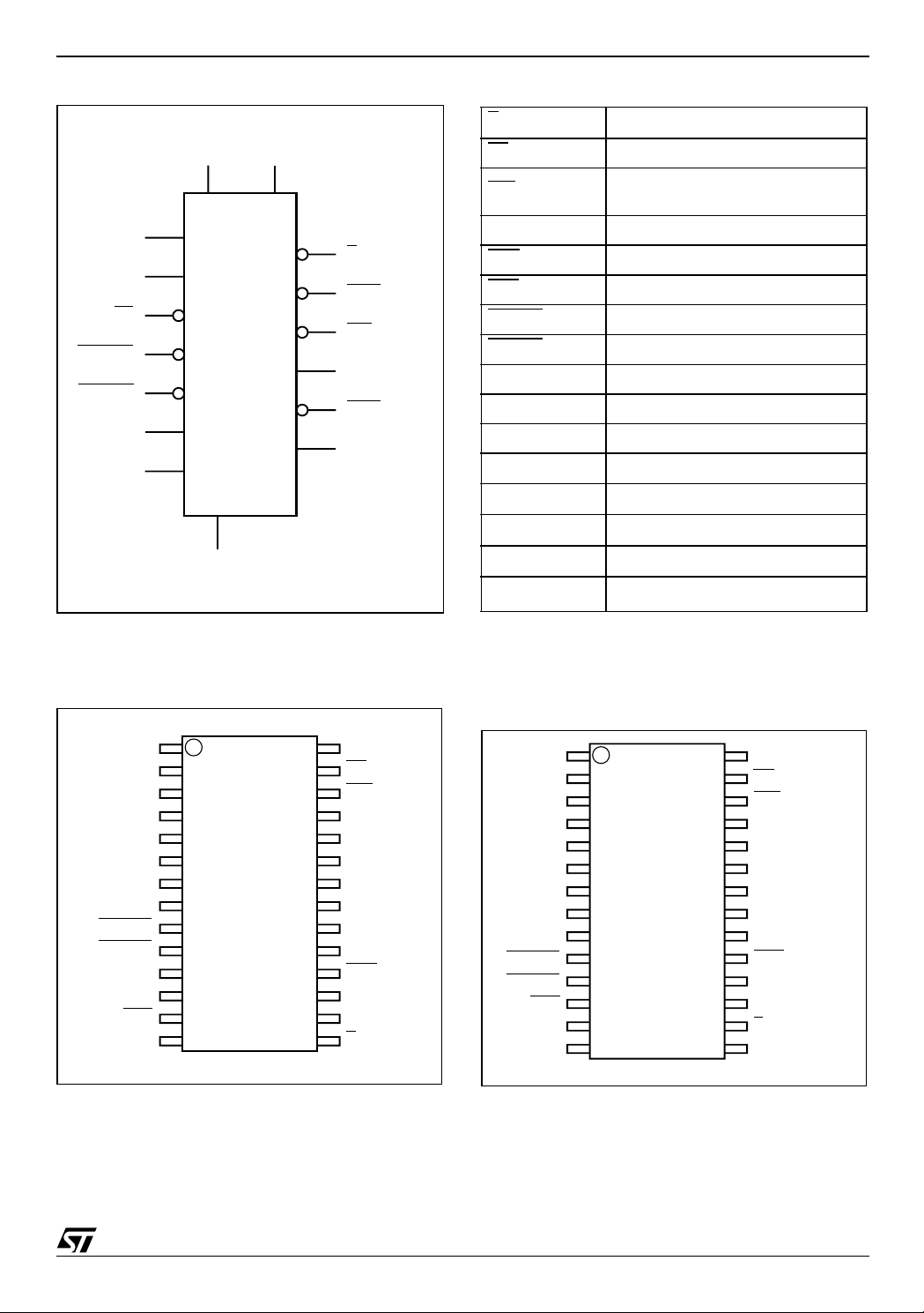
Figure 4. 28-pin SOIC Connections Figure 5. 28-pin, 300mil SOIC (MX)
Connections
SQW V
NC
NC
NC
NC
NC
NC
WDI
RSTIN1
RSTIN2
NC
1
2
3
4
5
6
7
M41ST85Y
M41ST85W
8
9
10
11
12
PFO
V
SS
13
14
28
27
26
25
24
23
22
21
20
19
18
17
16
15
AI03659
CC
EX
IRQ/FT/OUT
V
OUT
NC
NC
PFI
NC
SCL
NC
RST
NCNC
SDA
E
CON
NC V
NC
NC
NC
NC
NC
NC
SQW
WDI
RSTIN1
RSTIN2
PFO
NC
V
SS
1
2
3
4
5
6
7
M41ST85Y
M41ST85W
8
9
10
11
12
13
14
28
27
26
25
24
23
22
21
20
19
18
17
16
15
EX
IRQ/FT/OUT
V
V
PFI
SCL
NC
NC
RST
NC
SDA
E
V
CC
OUT
SS
CON
BAT
AI06370c
5/33
M41ST85Y, M41ST85W
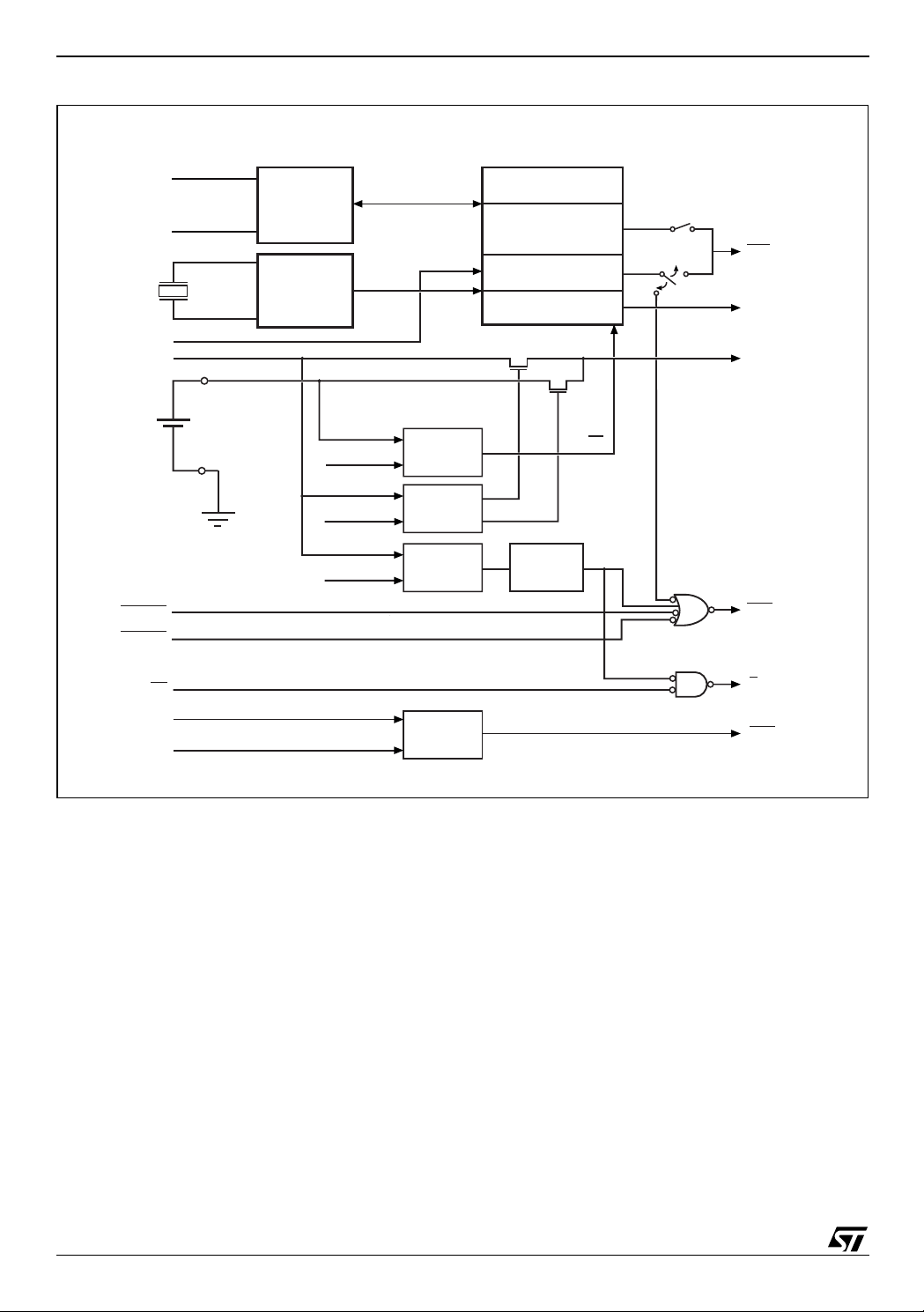
Figure 6. Block Diagram
SDA
SCL
(2)
Crystal
I2C
INTERFACE
32KHz
OSCILLA T OR
REAL TIME CLOCK
CALENDAR
44 BYTES
USER RAM
RTC w/ALARM
& CALIBRATION
WATCHDOG
SQUARE W AVE
AFE
WDS
IRQ/FT/OUT
SQW
(1)
WDI
V
CC
V
BA T
VBL= 2.5V
V
SO
V
PFD
RSTIN1
RSTIN2
EX
PFI
1.25V
(Internal)
Note: 1. Open drain output
2. Integra ted into SOIC package for MX package opt ion.
= 2.5V
= 4.4V
(2.65V for ST85W)
COMPARE
COMPARE
COMPARE
COMP ARE
POR
BL
V
OUT
RST
E
CON
PFO
(1)
AI03932
6/33
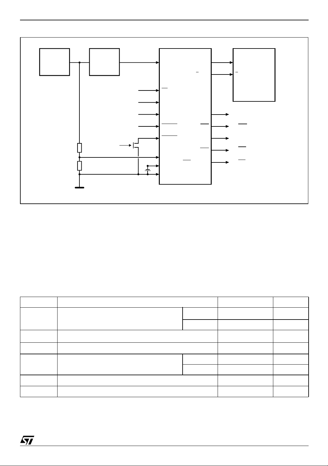
Figure 7. Hardware Hookup
M41ST85Y, M41ST85W
Unregulated
Voltage
R1
R2
Note: 1. Required for embedded crystal (MX) package only.
Regulator
V
V
IN
Pushbutton
Reset
CC
From MCU
MAXIMUM RATIN G
Stressing the device ab ove the rating listed in the
“Absolute Maximum Ratings” table may cause
permanent damage to the device. These are
stress ratings only and operation of the dev ice at
these or any other conditions above those indicated in the Operating sections of this specification is
M41ST85Y/W
V
CC
EX
SCL
WDI
RSTIN1
RSTIN2
PFI
V
BAT
V
SS
(1)
IRQ/FT/OUT
V
E
CON
SQW
OUT
SDA
RST
PFO
V
CC
E
M68Z128Y/W
or
M68Z512Y/W
To RST
To LED Display
To NMI
To INT
AI03660
not implied. Exposure to Absol ute Maxim um Ra ting conditions for extended periods may affect device reliability. Refer also to the
STMicroelectronics SURE Program and other relevant quality documents.
Table 2. Absolute Maximum Ratings
Symbol Parameter Value Unit
®
T
STG
Storage Temperature (VCC Off, Oscillator Off)
SNAPHAT
SOIC –55 to 125 °C
(1)
T
SLD
V
IO
V
CC
I
O
P
D
Note: 1. Reflow at peak temperature of 215°C to 225° C for < 60 sec onds (total thermal budg et not to exce ed 180°C for between 90 to 120
secon ds).
CAUTION: Negative und ershoots below –0.3V are not allowed on any pin while in the Bat tery Back-u p mode.
CAUTION: Do NOT wave solder SOIC to av oi d damaging SNAPHAT sockets.
Lead Solder Temperature for 10 seconds 260 °C
Input or Output Voltage
M41ST85Y –0.3 to 7 V
Supply Voltage
M41ST85W –0.3 to 4.6 V
Output Current 20 mA
Power Dissipation 1 W
–40 to 85 °C
–0.3 to V
CC
+0.3
V
7/33
M41ST85Y, M41ST85W
DC AND AC PARAMETERS
This section summarizes the operat ing and measurement conditions, as well as the DC and AC
characteristics of the device. The parameters in
the following DC and AC Characteristic tables are
derived from tests performed under the M easure-
Table 3. DC and AC Measurement Conditions
Parameter M41ST8 5Y M41ST85W
V
Supply Voltage
CC
Ambient Operating Temperature –40 to 85°C –40 to 85°C
Load Capacitance (C
)
L
Input Rise and Fall Times ≤ 50ns ≤ 50ns
Input Pulse Voltages
Input and Output Timing Ref. Voltages
Note: Output Hi gh Z is define d as the point where data is no l onger driven.
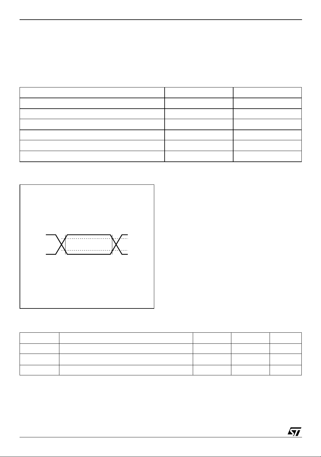
Figure 8. AC Testing Input/Output Waveforms
ment Conditions listed in the rel evant tables. Designers should check that the operating conditions
in their projects match the measurement conditions when using the quoted parameters.
4.5 to 5.5V 2.7 to 3.6V
100pF 50pF
0.2 to 0.8V
0.3 to 0.7V
CC
CC
0.2 to 0.8V
0.3 to 0.7V
CC
CC
0.8V
CC
0.2V
CC
Note: 50pF for M41ST85W.
0.7V
0.3V
AI02568
CC
CC
Table 4. Capacitance
Symbol
C
IN
(3)
C
OUT
t
LP
Note: 1. Effective capacitan ce measured wi th power supply at 5V. Sampled onl y, not 100% test ed.
2. At 25°C, f = 1MHz.
3. Outputs are deselect ed.
Input Capacitance 7 pF
Output Capacitance 10 pF
Low-pass filter input time constant (SDA and SCL) 50 ns
Parameter
(1,2)
Min Max Unit
8/33
Table 5. DC Characteristics
Sym Parameter
Battery Current OSC
ON
(2)
I
BAT
I
I
I
Battery Current OSC
OFF
Supply Current f = 400kHz 1.4 0.75 mA
CC1
Supply Current
CC2
(Standby)
Input Leakage Current
(3)
LI
Input Leakage Current
(PFI)
Test
Condition
= 25°C,
T
A
V
= 0V,
CC
= 3V
V
BAT
SCL, SDA =
– 0.3V
V
CC
0V ≤ V
≤
IN
V
CC
M41ST85Y, M41ST85W
M41ST85Y M41ST85W
(1)
Min Typ Max Min Typ Max
400 500 400 500 nA
50 50 nA
1 0.50 mA
±1 ±1 µA
–25 2 25 –25 2 25 nA
Unit
I
LO
I
OUT1
I
OUT2
V
V
V
OHB
V
V
V
VCC – 0.3V
V
(6)
IOH = –1.0mA
I
IOL = 10mA
V
VCC = 3V(V)
0V ≤ V
BAT
OL
CC
Output Leakage
(4)
Current
(5)
V
Current (Active)
OUT
V
Current (Battery
OUT
Back-up)
V
Input High Voltage
IH
V
Input Low Voltage –0.3
IL
Battery Voltage 2.5 3.0
BAT
OH
Output High Voltage
(7)
VOH (Battery Back-up)
Output Low Voltage
OL
Output Low Voltage
(Open Drain)
Power Fail Deselect 4.20 4.40 4.50 2.55 2.60 2.70 V
PFD
(8)
PFI Input Threshold
PFI
IN
V
CC
V
OUT1
V
OUT2
– 0.3V
=
I
OUT2
–1.0µA
= 3.0mA
= 5V(Y)
>
>
≤
±1 ±1 µA
175 100 mA
100 100 µA
0.7V
CC
VCC + 0.3 0.7V
0.3V
3.5
CC
(9)
–0.3
2.5 3.0
CC
2.4 2.4 V
2.5 2.9 3.5 2.5 2.9 3.5 V
0.4 0.4 V
0.4 0.4 V
1.225 1.250 1.275 1.225 1.250 1.275 V
VCC + 0.3
0.3V
3.5
PFI Hysteresis PFI Rising 20 70 20 70 mV
V
Note: 1. Valid for A m bi ent Operat in g T em perature: TA = –40 to 85°C ; VCC = 4.5 to 5.5V or 2. 7 to 3.6V (exce pt where noted) .
Battery Back-up
SO
Switchover
2. Measured with V
3. RSTIN1
4. Outputs Dese l ected .
5. External SRAM must match RTC SUPERVISOR chip V
6. For PFO
7. Conditi oned outp ut (E
8. For IRQ
9. For rech argeable back-up, V
and RSTI N2 internally pulled-up t o VCC through 100KΩ resistor. WDI internally pulled-down to VSS through 100KΩ resistor.
and SQW pins (CMOS) .
duce batter y li fe.
/FT/OUT, RST pins (Ope n Drai n): i f pu ll ed- up to supp ly oth e r tha n VCC, this su ppl y mu st be equ al to, or l es s t han 3. 0V when
V
= 0V (durin g battery back -up mode).
CC
OUT
and E
CON
open.
CON
) can only sust ain CMOS le akage curren t in the ba tter y ba ck-u p mode . Highe r leak ag e curre nts w ill re -
(max) may be considered VCC.
BAT
specification.
CC
2.5 2.5 V
(9)
CC
V
V
V
9/33

M41ST85Y, M41ST85W
OPERATING MODES
The M41ST85Y/W clock operates as a slave device on the serial bus. Access is obtained by implementing a start condition followed by the
correct slave address (D0h). The 64 bytes contained in the device can then be accessed sequentially in the following order:
1. Tenths/Hundredths of a Second Register
2. Seconds Register
3. Minutes Register
4. Century/Hours Register
5. Day Register
6. Date Register
7. Month Register
8. Year Register
9. Control Register
10. Watchdog Register
11 - 16. Alarm Registers
17 - 19. Reserved
20. Square Wave Register
21 - 64. User RAM
The M41ST85Y/W clock continually monitors V
for an out-of-tolerance condition. Should VCC fall
below V
, the device terminates an access in
PFD
progress and resets t he device address counter.
Inputs to the device will not be recognized at this
time to prevent erroneous dat a f rom bei ng wri tten
to the device from a an out-of-tolerance system.
When V
falls below VSO, the device a utomati-
CC
cally switches over to the battery and powers
down into an ultra low current mode of operation to
CC
conserve bat tery life. As system p ower returns an d
rises above VSO, the battery is disconnected,
V
CC
and the power supply is switched to external V
Write protection continues until V
V
(min) plus t
PFD
REC
(min).
CC
CC
reaches
For more information on Battery Storage Life refer
to Application Note AN1012.
2-Wire Bus Characteristics
The bus is intended for communication between
different ICs. It consists of two lines: a bi-directional data signal (SDA) and a clock signal (SCL).
Both the SDA and SCL lines must be connected to
a positive supply voltage via a pull-up resistor.
The following protocol has been defined:
– Data transfer may be initiated only when the bus
is not busy.
– During data transfer, the data line must remain
stable whenever the clock line is High.
– Changes in the data line, while the clock line is
High, will be interpreted as control signals.
Accordingly, the following bus conditions have
been defined:
Bus not busy. Both data and clock lines remain
High.
Start data transfer. A c hange in the st ate of the
data line, from High to Low, while the clock is High,
defines the START condition.
Stop data transfer. A change in the state of the
data line, from Low to High, while the clock is High,
defines the STOP condition.
.
10/33
 Loading...