

SGS Thomson Microelectronics M41ST84Y, M41ST84W Datasheet
5.0 or 3.0V, 512 bit (64 x 8) SERIAL RTC
with SUPERVISORY FUNCTIONS
FEATURES SUMMARY
■ 5.0 OR 3.0V OPERATING VO LTA G E
■ SERIAL INTERFACE SU PPO R TS I
(400 KHz)
■ OPTIMIZED FOR MINIMAL INTERCONNECT
TO MCU
■ 2.5 TO 5.5V OSCILLATOR OPERATING
VOLTAGE
■ AUTOMATIC SWITCH-OVER and DESELECT
CIRCUITRY
■ CHOICE OF POWER-FAIL DESELECT
VOLTAGES:
– M41ST84Y : V
4.20V ≤ V
– M41ST84W: V
2.55V ≤ V
■ 1.25V REFERENCE (for PFI/PFO)
■ COUNTERS FOR TENTHS/HUNDREDTHS
PFD
PFD
= 4.5 to 5.5V;
CC
≤ 4.50V
= 2.7 to 3.6V;
CC
≤ 2.70V
OF SECONDS, SECONDS, MINUTES,
HOURS, DAY, DATE , MONTH, YEAR, and
CENTURY
■ 44 BYTES OF GENERAL PURPOSE RAM
■ PROGRAMMABLE ALARM and INTE RRUPT
FUNCTION (VALID EVEN DURING BATTERY
BACK-UP MODE)
■ WATCHDOG T IME R
■ MICROPROCESSOR POWER-ON RESET
■ BATTERY LOW FLAG
■ ULTRA-LOW BATT ERY SU PPL Y C URRE N T
OF 500 nA (m ax)
■ OPTIONAL PACKAGING INCLUDES A 28-
LEAD SOIC and SNAPHAT
®
ordered separately)
■ SNAPHAT PACKAGE PROVIDES DIRECT
CONNECTION FOR A SNAPHAT TOP,
WHICH CONTAINS THE BATTERY and
CRYSTAL
2
C BUS
TOP (to be
M41ST84Y
M41ST84W
Figure 1. 16-pi n S O I C Package
16
1
SO16 (MQ)
Figure 2. 28-pi n S O I C Package*
SNAPHAT (SH)
Battery & Crystal
28
1
SOH28 (MH)
* Contact Local Sales Office
Rev. 4.0
1/31June 2003

M41ST84Y, M41ST84W
TABLE OF CONTENTS
SUMMARY DESCRIPTION. . . . . . . . . . . . . . . . . . . . . . . . . . . . . . . . . . . . . . . . . . . . . . . . . . . . . . . . . . . 4
Figure 3. Logic Diagram . . . . . . . . . . . . . . . . . . . . . . . . . . . . . . . . . . . . . . . . . . . . . . . . . . . . . . . . . . 4
Table 1. Signal Names . . . . . . . . . . . . . . . . . . . . . . . . . . . . . . . . . . . . . . . . . . . . . . . . . . . . . . . . . . . 4
Figure 4. 16-pin SOIC Connections. . . . . . . . . . . . . . . . . . . . . . . . . . . . . . . . . . . . . . . . . . . . . . . . . . 5
Figure 5. 28-pin SOIC Connections. . . . . . . . . . . . . . . . . . . . . . . . . . . . . . . . . . . . . . . . . . . . . . . . . . 5
Figure 6. Block Diagram . . . . . . . . . . . . . . . . . . . . . . . . . . . . . . . . . . . . . . . . . . . . . . . . . . . . . . . . . . 5
Figure 7. Hardware Hookup . . . . . . . . . . . . . . . . . . . . . . . . . . . . . . . . . . . . . . . . . . . . . . . . . . . . . . . 6
MAXIMUM RATING. . . . . . . . . . . . . . . . . . . . . . . . . . . . . . . . . . . . . . . . . . . . . . . . . . . . . . . . . . . . . . . . . 6
Table 2. Absolute Maximum Ratings. . . . . . . . . . . . . . . . . . . . . . . . . . . . . . . . . . . . . . . . . . . . . . . . . 6
DC AND AC PARAMETERS. . . . . . . . . . . . . . . . . . . . . . . . . . . . . . . . . . . . . . . . . . . . . . . . . . . . . . . . . . 7
Table 3. DC and AC Measurement Conditions . . . . . . . . . . . . . . . . . . . . . . . . . . . . . . . . . . . . . . . . . 7
Figure 8. AC Testing Input/Output Waveforms . . . . . . . . . . . . . . . . . . . . . . . . . . . . . . . . . . . . . . . . . 7
Table 4. Capacitance. . . . . . . . . . . . . . . . . . . . . . . . . . . . . . . . . . . . . . . . . . . . . . . . . . . . . . . . . . . . . 7
Table 5. DC Characteristics. . . . . . . . . . . . . . . . . . . . . . . . . . . . . . . . . . . . . . . . . . . . . . . . . . . . . . . . 8
Table 6. Crystal Electrical Characteristics (Externally Supplied) . . . . . . . . . . . . . . . . . . . . . . . . . . . .8
OPERATING MODES . . . . . . . . . . . . . . . . . . . . . . . . . . . . . . . . . . . . . . . . . . . . . . . . . . . . . . . . . . . . . . . 9
2-Wire Bus Characteristics. . . . . . . . . . . . . . . . . . . . . . . . . . . . . . . . . . . . . . . . . . . . . . . . . . . . . . . 9
Figure 9. Serial Bus Data Transfer Sequence. . . . . . . . . . . . . . . . . . . . . . . . . . . . . . . . . . . . . . . . . 10
Figure 10. Acknowledgement Sequence. . . . . . . . . . . . . . . . . . . . . . . . . . . . . . . . . . . . . . . . . . . . . 10
Figure 11. Bus Timing Requirements Sequence. . . . . . . . . . . . . . . . . . . . . . . . . . . . . . . . . . . . . . . 10
Table 7. AC Characteristics. . . . . . . . . . . . . . . . . . . . . . . . . . . . . . . . . . . . . . . . . . . . . . . . . . . . . . . 11
READ Mode . . . . . . . . . . . . . . . . . . . . . . . . . . . . . . . . . . . . . . . . . . . . . . . . . . . . . . . . . . . . . . . . . . 12
Figure 12. Slave Address Location . . . . . . . . . . . . . . . . . . . . . . . . . . . . . . . . . . . . . . . . . . . . . . . . . 1 2
Figure 13. READ Mode Sequence . . . . . . . . . . . . . . . . . . . . . . . . . . . . . . . . . . . . . . . . . . . . . . . . . 12
Figure 14. Alternate READ Mode Sequence. . . . . . . . . . . . . . . . . . . . . . . . . . . . . . . . . . . . . . . . . . 13
WRITE Mode. . . . . . . . . . . . . . . . . . . . . . . . . . . . . . . . . . . . . . . . . . . . . . . . . . . . . . . . . . . . . . . . . . 13
Figure 15. WRITE Mode Sequence . . . . . . . . . . . . . . . . . . . . . . . . . . . . . . . . . . . . . . . . . . . . . . . . . 13
Data Retention Mode. . . . . . . . . . . . . . . . . . . . . . . . . . . . . . . . . . . . . . . . . . . . . . . . . . . . . . . . . . . 14
Figure 16. Power Down/Up Mode AC Waveforms . . . . . . . . . . . . . . . . . . . . . . . . . . . . . . . . . . . . . 14
Table 8. Power Down/Up AC Characteristics . . . . . . . . . . . . . . . . . . . . . . . . . . . . . . . . . . . . . . . . . 14
CLOCK OPERATION . . . . . . . . . . . . . . . . . . . . . . . . . . . . . . . . . . . . . . . . . . . . . . . . . . . . . . . . . . . . . . 15
TIMEKEEPER® Registers. . . . . . . . . . . . . . . . . . . . . . . . . . . . . . . . . . . . . . . . . . . . . . . . . . . . . . . 15
Table 9. TIMEKEEPER® Register Map . . . . . . . . . . . . . . . . . . . . . . . . . . . . . . . . . . . . . . . . . . . . . 16
Calibrating the Clock. . . . . . . . . . . . . . . . . . . . . . . . . . . . . . . . . . . . . . . . . . . . . . . . . . . . . . . . . . . 1 7
2/31

M41ST84Y, M41ST84W
Setting Alarm Clock Registers. . . . . . . . . . . . . . . . . . . . . . . . . . . . . . . . . . . . . . . . . . . . . . . . . . . 18
Figure 17. Alarm Interrupt Reset Waveform . . . . . . . . . . . . . . . . . . . . . . . . . . . . . . . . . . . . . . . . . .18
Table 10. Alarm Repeat Modes. . . . . . . . . . . . . . . . . . . . . . . . . . . . . . . . . . . . . . . . . . . . . . . . . . . . 18
Figure 18. Back-Up Mode Alarm Waveform . . . . . . . . . . . . . . . . . . . . . . . . . . . . . . . . . . . . . . . . . . 19
Watchdog Timer . . . . . . . . . . . . . . . . . . . . . . . . . . . . . . . . . . . . . . . . . . . . . . . . . . . . . . . . . . . . . . 19
Square Wave Outp ut . . . . . . . . . . . . . . . . . . . . . . . . . . . . . . . . . . . . . . . . . . . . . . . . . . . . . . . . . . . 20
Table 11. Square Wave Output Frequency . . . . . . . . . . . . . . . . . . . . . . . . . . . . . . . . . . . . . . . . . . .20
Power-on Reset . . . . . . . . . . . . . . . . . . . . . . . . . . . . . . . . . . . . . . . . . . . . . . . . . . . . . . . . . . . . . . . 21
Reset Input (RSTIN). . . . . . . . . . . . . . . . . . . . . . . . . . . . . . . . . . . . . . . . . . . . . . . . . . . . . . . . . . . . 21
Figure 19. RSTIN Timing Waveform. . . . . . . . . . . . . . . . . . . . . . . . . . . . . . . . . . . . . . . . . . . . . . . . 21
Reset AC Characteristics . . . . . . . . . . . . . . . . . . . . . . . . . . . . . . . . . . . . . . . . . . . . . . . . . . . . . . . 2 1
Power-fail INPUT/OUTPUT . . . . . . . . . . . . . . . . . . . . . . . . . . . . . . . . . . . . . . . . . . . . . . . . . . . . . . 22
Century Bit. . . . . . . . . . . . . . . . . . . . . . . . . . . . . . . . . . . . . . . . . . . . . . . . . . . . . . . . . . . . . . . . . . . 22
Output Driver Pin. . . . . . . . . . . . . . . . . . . . . . . . . . . . . . . . . . . . . . . . . . . . . . . . . . . . . . . . . . . . . .22
Battery Low Warning. . . . . . . . . . . . . . . . . . . . . . . . . . . . . . . . . . . . . . . . . . . . . . . . . . . . . . . . . . . 2 2
t
Bit . . . . . . . . . . . . . . . . . . . . . . . . . . . . . . . . . . . . . . . . . . . . . . . . . . . . . . . . . . . . . . . . . . . . . . 22
REC
Initial Power-on Defaults. . . . . . . . . . . . . . . . . . . . . . . . . . . . . . . . . . . . . . . . . . . . . . . . . . . . . . . . 2 2
Table 13. t
Definitions . . . . . . . . . . . . . . . . . . . . . . . . . . . . . . . . . . . . . . . . . . . . . . . . . . . . . . . . 23
REC
Table 14. Default Values. . . . . . . . . . . . . . . . . . . . . . . . . . . . . . . . . . . . . . . . . . . . . . . . . . . . . . . . . 23
Figure 20. Crystal Accuracy Across Temperature. . . . . . . . . . . . . . . . . . . . . . . . . . . . . . . . . . . . . . 24
Figure 21. Clock Calibration . . . . . . . . . . . . . . . . . . . . . . . . . . . . . . . . . . . . . . . . . . . . . . . . . . . . . . 24
PACKAGE MECHANICAL INFORMATION . . . . . . . . . . . . . . . . . . . . . . . . . . . . . . . . . . . . . . . . . . . . . 25
PART NUMBERING . . . . . . . . . . . . . . . . . . . . . . . . . . . . . . . . . . . . . . . . . . . . . . . . . . . . . . . . . . . . . . . 29
Table 20. SNAPHAT Battery Table . . . . . . . . . . . . . . . . . . . . . . . . . . . . . . . . . . . . . . . . . . . . . . . . .29
REVISION HISTORY . . . . . . . . . . . . . . . . . . . . . . . . . . . . . . . . . . . . . . . . . . . . . . . . . . . . . . . . . . . . . . . 30
3/31
M41ST84Y, M41ST84W
SUMMARY DESCRIPTION
The M4 1S T84 Y/W Seria l supervi s o r y TIMEKEE P-
®
SRAM is a low power 512-bit static CMOS
ER
SRAM organized as 64 words by 8 bi ts. A built-in
32.768 kHz oscilla tor (external crystal controlled)
and 8 bytes of the SRAM (see Table 9, page 16)
are used for the c lock/calendar function and are
configured in binary coded decimal (BCD) format.
An additional 12 bytes of RAM provide status/control of Alarm, Watchdog and Sq uare Wave functions. Addresses and data are transferred serially
via a two line, bi-directional I2C interface. The
built-in address register is incremented automatically after each WRITE or READ data byte.
The M41ST84Y/W has a built-in power sense circuit which detects power failures and automatically switches to the battery supply when a power
failure occurs. The energy needed to s ustain the
SRAM and clock operations can be supplied by a
small lithium button-cell supply when a power failure occurs. Functions available to the user include
a non-volatile, time-of-day clock/calendar, Alarm
interrupts, Watchdog Timer and programmable
Square Wave output. Other features include a
Power-On Reset as well as an additional input
(RSTIN
(RST
the century, year, month, dat e, day , hour, minute,
second and tenths/hun dredths of a second in 24
) which can also generate an output Reset
). The eight clock address locations contain
hour BCD format. Corrections for 28, 29 (leap year
- valid until year 2100), 30 and 31 day months are
made aut omatically.
The M41ST84Y/W is supplied in a 28-lead SOIC
SNAPHAT
®
package (which integrates b oth crystal and battery in a single SNAP HA T top) or a 16pin SOIC. The 28-pin, 330mil SOIC provides sockets with gold plated contacts at both ends for direct
connection to a separate SNAPHAT housing containing the battery and crystal. The unique design
allows the SNAPHAT battery/crystal package to
be mounted on top of the S OIC pack age after t he
completion of the surface mount process.
Insertion of the SNAPHAT housing after reflow
prevents potential battery and crystal damage due
to the high temperatures required for device surface-mounting. The SNAPHAT housing is also
keyed to prevent reverse insertion.
The 28-pin SOIC and battery/crystal packages are
shipped separately in plastic anti-static tubes or in
Tape & Reel form. For the 2 8-lead SOIC, t he ba ttery/crystal package (e.g., SNAPHAT) part number is “M4TXX-BR12SH” (see Table 20, page 29).
Caution: Do not place the SNAPHAT battery/crystal top in conductive foam, as this will drain the lithium button-cell battery.
Figure 3. Logic Diagram
V
V
CC
(1)
XI
(1)
XO
SCL
SDA
RSTIN
WDI
PFI
Note: 1. For SO16 package only.
M41ST84Y
M41ST84W
V
SS
BAT
(1)
RST
IRQ/FT/OUT
SQW
PFO
AI03677
Table 1. Signal Names
(1)
XI
(1)
XO
IRQ
/FT/OUT
PFI Power Fail Input
PFO
RST
RSTIN
SCL Serial Clock Input
SDA Serial Data Input/Output
SQW Square Wave Output
WDI Watchdog Input
V
CC
(1)
V
BAT
V
SS
Note: 1. For SO16 package only.
Oscillator Input
Oscillator Output
Interrupt/Frequency Test/Out
Output (Open Drain)
Power Fail Output
Reset Output (Open Drain)
Reset Input
Supply Voltage
Battery Supply Voltage
Ground
4/31
M41ST84Y, M41ST84W
Figure 4. 16-pi n S O I C Co nnections Figure 5. 28-pi n S O I C C onnections
1
XI V
XO
RST
WDI
RSTIN
PFO
V
BAT
V
SS
2
3
4
M41ST84Y
M41ST84W
5
6
7
8
Figure 6. Block Diagram
SDA
SCL
Crystal
16
15
14
13
12
11
10
9
AI03678
I2C
INTERFACE
32KHz
OSCILLA T OR
CC
NC
IRQ/FT/OUT
NC
PFI
SQW
SCL
SDA
SQW V
NC
NC
NC
NC
NC
NC
WDI
RSTIN
NC
NC
1
2
3
4
5
6
7
M41ST84Y
M41ST84W
8
9
10
11
12
PFO
V
SS
REAL TIME CLOCK
CALENDAR
44 BYTES
USER RAM
RTC w/ALARM
& CALIBRATION
WATCHDOG
SQUARE W AVE
13
14
AF
WDF
28
27
26
25
24
23
22
21
20
19
18
17
16
15
AI03679
CC
NC
IRQ/FT/OUT
NC
NC
NC
PFI
NC
SCL
NC
RST
NCNC
SDA
NC
IRQ/FT/OUT
SQW
(1)
WDI
V
CC
V
BA T
RSTIN
PFI
1.25V
(Internal)
Note: 1. Open dra i n out put
VBL= 2.5V
V
SO
V
PFD
COMPARE
= 2.5V
= 4.4V
COMPARE
COMPARE
(2.65V for ST84W)
COMP ARE
POR
BL
POWER
(1)
RST
PFO
AI03931
5/31
M41ST84Y, M41ST84W
Figure 7. Hardware Hookup
Unregulated
Voltage
R1
R2
Regulator
V
IN
V
CC
From MCU
MAXIMUM RATIN G
Stressing the device ab ove the rating listed in the
“Absolute Maximum Ratings” table may cause
permanent damage to the device. These are
stress ratings only and operation of the dev ice at
these or any other conditions above those indicated in the Operating sections of this specification is
M41ST84Y/W
V
SCL
WDI
RSTIN
PFI
V
CC
SS
IRQ/FT/OUT
SDA
RST
SQW
PFO
To INT
To RST
To LED Display
To NMI
AI03680
not implied. Exposure to Absol ute Maxim um Ra ting conditions for extended periods may affect device reliability. Refer also to the
STMicroelectronics SURE Program and other relevant quality documents.
Table 2. Absolute Maximum Ratings
Symbol Parameter Value Unit
®
T
STG
Storage Temperature (VCC Off, Oscillator Off)
SNAPHAT
SOIC –55 to 125 °C
(1)
T
SLD
V
IO
Lead Solder Temperature for 10 seconds 260 °C
Input or Output Voltages
M41ST84Y –0.3 to 7.0 V
V
CC
I
O
P
D
Note: 1. Reflow at peak temperature of 215°C to 225° C f or < 60 seconds (total thermal budg et not to exce ed 180°C for between 90 to 120
CAUTION: Negative undershoots below –0.3V are not allowed on any pin while in the Battery Back-up mode.
CAUTION: Do NOT wave sol der SOIC to av oi d damaging S NAPHAT sockets.
Supply Voltage
M41ST84W –0.3 to 4.6 V
Output Current 20 mA
Power Dissipation 1 W
secon ds).
6/31
–40 to 85 °C
–0.3 to V
CC
+ 0.3
V
M41ST84Y, M41ST84W
DC AND AC PARAMETERS
This section summarizes the operat ing and measurement conditions, as well as the DC and AC
characteristics of the device. The parameters in
the following DC and AC Characteristic tables are
derived from tests performed under the M easure-
Table 3. DC and AC Measurement Conditions
Parameter M41ST84Y M41ST84W
V
Supply Voltage
CC
Ambient Operating Temperature –40 to 85°C –40 to 85°C
Load Capacitance (C
)
L
Input Rise and Fall Times ≤ 50ns ≤ 50ns
Input Pulse Voltages
Input and Output Timing Ref. Voltages
Note: Output Hi-Z is defi ned as the point where data i s no longer dri ven.
Figure 8. AC Testing Input/Output Waveforms
ment Conditions listed in the rel evant tables. Designers should check that the operating conditions
in their projects match the measurement conditions when using the quoted parameters.
4.5 to 5.5V 2.7 to 3.6V
100pF 50pF
0.2 to 0.8V
0.3 to 0.7V
CC
CC
0.2 to 0.8V
0.3 to 0.7V
CC
CC
0.8V
CC
0.2V
CC
Note: 50pF f or M41ST84 W.
0.7V
0.3V
AI02568
CC
CC
Table 4. Capacitance
Symbol
C
IN
C
IO
t
LP
Note: 1. Effectiv e capacitan ce measured wi th power su pply at 5V. Sampled only, not 100% tested.
2. At 25°C, f = 1MHz.
3. Outputs deselected .
Input Capacitance 7 pF
(3)
Input / Output Capacitance 10 pF
Low-pass filter input time constant (SDA and SCL) 50 ns
Parameter
(1,2)
Min Max Unit
7/31
M41ST84Y, M41ST84W
Table 5. DC Characteristics
Sym Parameter
Battery Current OSC
ON
I
BAT
Battery Current OSC
OFF
I
Supply Current f = 400kHz 1.4 0.75 mA
CC1
Supply Current
I
CC2
(Standby)
Input Leakage Current
(2)
I
LI
Input Leakage Current
Test
Condition
= 25°C,
T
A
VCC = 0V,
V
= 3V
BAT
SCL, SDA =
– 0.3V
V
CC
0V ≤ V
IN
≤ V
(1)
CC
(PFI)
Output Leakage
(3)
I
LO
Current
V
Input High Voltage
IH
V
Input Low Voltage –0.3
IL
V
Battery Voltage 2.5 3.0
BAT
V
OH
Output High Voltage
Output Low Voltage
V
OL
Output Low Voltage
(Open Drain)
V
Power Fail Deselect 4 .20 4.40 4.50 2 .55 2.60 2.70 V
PFD
PFI Input Threshold
V
PFI
(5)
(4)
0V ≤ V
IOH = –1.0mA
I
IOL = 10mA
V
VCC = 3V(V)
OUT
= 3.0mA
OL
= 5V(Y)
CC
≤ V
CC
0.7V
PFI Hysteresis PFI Rising 20 70 20 70 mV
Battery Back-up
V
SO
Switchover
Note: 1. Valid for Ambient Operating Temperature : TA = –40 to 85°C ; VCC = 2.7 to 3.6V or 4. 5 to 5.5V (except where noted).
2. RSTI N
3. Outputs deselected .
4. For PFO
5. For IRQ
6. For rechargeable back-up, V
internally pulled-up to VCC through 100KΩ resist or. WDI internally pulled- down to VSS through 100K Ω resistor.
and SQW pins (CMOS) .
/FT/OUT, RST pins (Ope n Drai n): i f pu ll ed- up to supp ly oth e r tha n VCC, this su ppl y mu st be equ al to, or l es s t han 3. 0V when
V
= 0V (durin g battery back-up mode).
CC
(max) may be considered VCC.
BAT
M41ST84Y M41ST84W
Min Typ Max Min Typ Max
400 500 400 500 nA
50 50 nA
1 0.50 mA
±1 ±1 µA
–25 2 25 –25 2 25 nA
±1 ±1 µA
CC
VCC + 0.3 0.7V
0.3V
3.5
(6)
CC
–0.3
2.5 3.0
CC
VCC + 0.3
0.3V
3.5
2.4 2.4 V
0.4 0.4 V
0.4 0.4 V
1.225 1.250 1.275 1.225 1.250 1.275 V
2.5 2.5 V
(6)
CC
Unit
V
V
V
Table 6. Crystal Electrical Characteristics (Externally Supplied)
Symbol
f
0
R
S
C
L
Note: 1. Load capacitors are integrated within the M41ST84Y/W. Circuit board layout considerations for the 32.768 kHz crystal of minimum
trace lengths and isolat i on from RF generating signals should be ta ken into account.
2. STMicroelectronics recommends the KDS DT-38: 1TA/1TC252E127, Tuning Fork Type (thru-hole) or the DMX-26S:
1TJS125 F H2A212, (SMD) quartz cry st al for indust ri al temperatur e operations. KDS can be contacted at k ouhou@kdsj .co.jp or http://www.kdsj.co.jp for further information on this crystal type.
Resonant Frequency 32.768 kHz
Series Resistance 50 kΩ
Load Capacitance 12.5 pF
Parameter
(1,2)
8/31
Typ Min Max Unit

OPERATING MODES
The M41ST84Y/W clock operates as a slave device on the serial bus. Access is obtained by implementing a start condition followed by the
correct slave address (D0h). The 64 bytes contained in the device can then be accessed sequentially in the following order:
1. Tenths/Hundredths of a Second Register
2. Seconds Register
3. Minutes Register
4. Century/Hours Register
5. Day Register
6. Date Register
7. Month Register
8. Year Register
9. Control Register
10. Watchdog Register
11 - 16. Alarm Registers
17 - 19. Reserved
20. Square Wav e Regi ster
21 - 64. User RAM
The M41ST84Y/W clock continually monitors V
CC
for an out-of tolerance condition. Should VCC fall
below V
, the device terminates an access in
PFD
progress and resets t he device address counter.
Inputs to the device will not be recognized at this
time to prevent erroneous dat a f rom bei ng wri tten
to the device from a an out-of-tolerance system.
When V
falls below VSO, the device a utomati-
CC
cally switches over to the battery and powers
down into an ultra low current mode of operation to
conserve bat tery life. As system p ower returns an d
V
rises above VSO, the battery is disconnected,
CC
and the power supply is switched to external V
Write protection continues until V
V
PFD
(min) plus t
REC
(min).
CC
CC
reaches
For more information on Battery Storage Life refer
to Application Note AN1012.
2-Wire Bus Characteristics
The bus is intended for communication between
different ICs. It consists of two lines: a bi-directional data signal (SDA) and a clock signal (SCL).
Both the SDA and SCL lines must be connected to
a positive supply voltage via a pull-up resistor.
The following protocol has been defined:
– Data transfer may be initiated only when the bus
is not busy.
– During data trans fer, the dat a line mus t remain
stable whenever the clock line is High.
M41ST84Y, M41ST84W
– Changes in the data line, while the clock line is
High, will be interpreted as control signals.
Accordingly, the following bus conditions have
been defined:
Bus not busy. Both data and clock lines remain
High.
Start data transfer. A c hange in the st ate of the
data line, from High to Low, while the clock is High,
defines the START condition.
Stop data transfer. A change in the state of the
data line, from Low to High, while the clock is High,
defines the STOP condition.
Data Valid. The state of the data line represents
valid data when after a start condition, the data line
is stable for the duration of the high period of the
clock signal. The data on the line may be changed
during the Low period of the clock signal. There is
one clock pulse per bit of data.
Each data transfer is initiated with a start condition
and terminated with a stop condition. The number
of data bytes transferred between the start and
stop conditions is not limited. The information is
transmitted byte-wide and each receiver acknowledges with a ninth bit.
By definition a device that gives out a message is
called “transmitter”, the receiving device that gets
the message is called “receiver”. The device that
controls the message is called “master”. The devices that are controlled by the master are cal led
“slaves”.
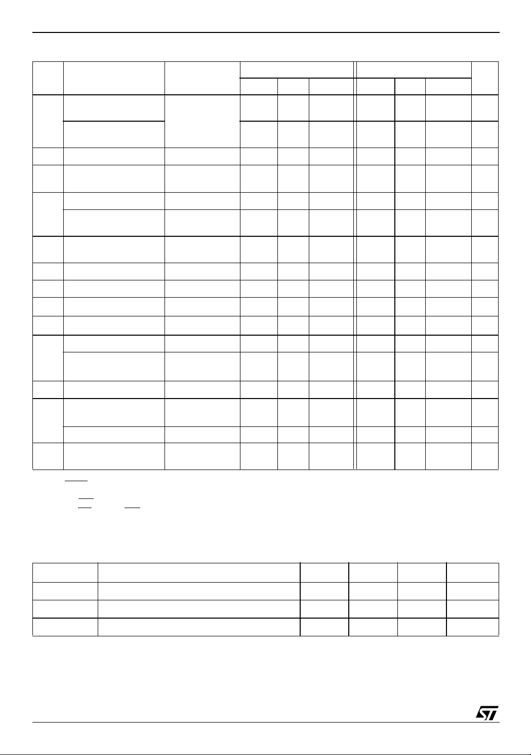
Acknowledge. Each byte of eight bits is followed
by one Acknowledge Bit. This Acknowledge Bit is
a low level put on the bus by the receiver whereas
the master generates an extra acknowledge relat-
.
ed clock pulse. A slave receiver which is addressed is obliged to generate an acknowledge
after the reception of each byte that has been
clocked out of the slave transmitter.
The device that acknowledges has to pull down
the SDA line during the acknowledge clock pulse
in such a way that the SDA line is a stable Low during the High period of the acknowledge related
clock pulse. Of course, setup and hold times must
be taken into account. A master receiver must signal an end of data to the slave transm itter by not
generating an acknowledge on t he last byte that
has been clocked out of the slave. In this case the
transmitter must leave the data line High to enable
the master to generate the STOP condition.
9/31
M41ST84Y, M41ST84W
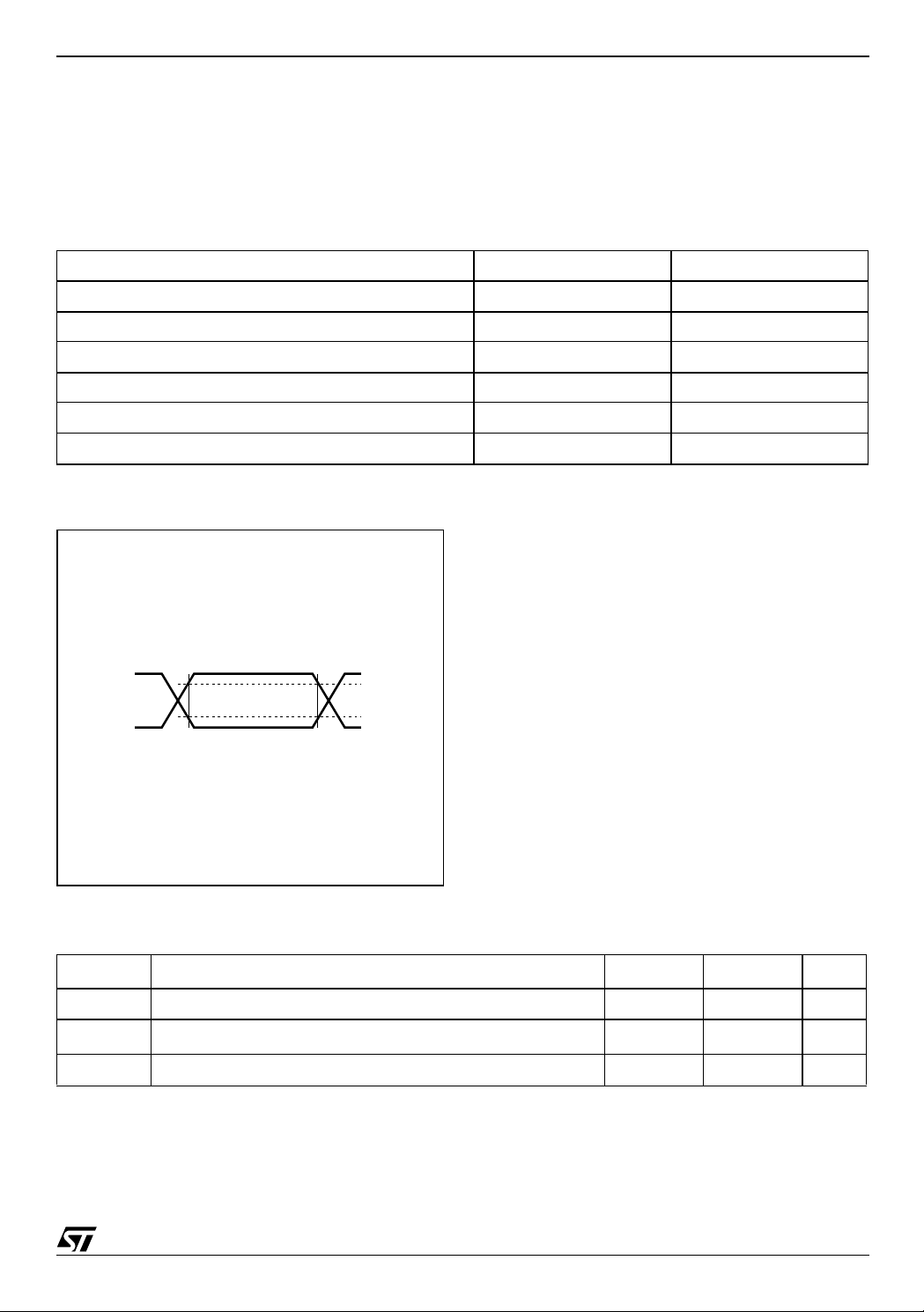
Figure 9. Serial Bus Data Transfer Sequence
DATA LINE
STABLE
DATA VALID
CLOCK
DATA
START
CONDITION
DATA ALLOWED
Figure 10. Acknowledgement Sequence
START
SCLK FROM
MASTER
DATA OUTPUT
BY TRANSMITTER
12 89
MSB LSB
DATA OUTPUT
BY RECEIVER
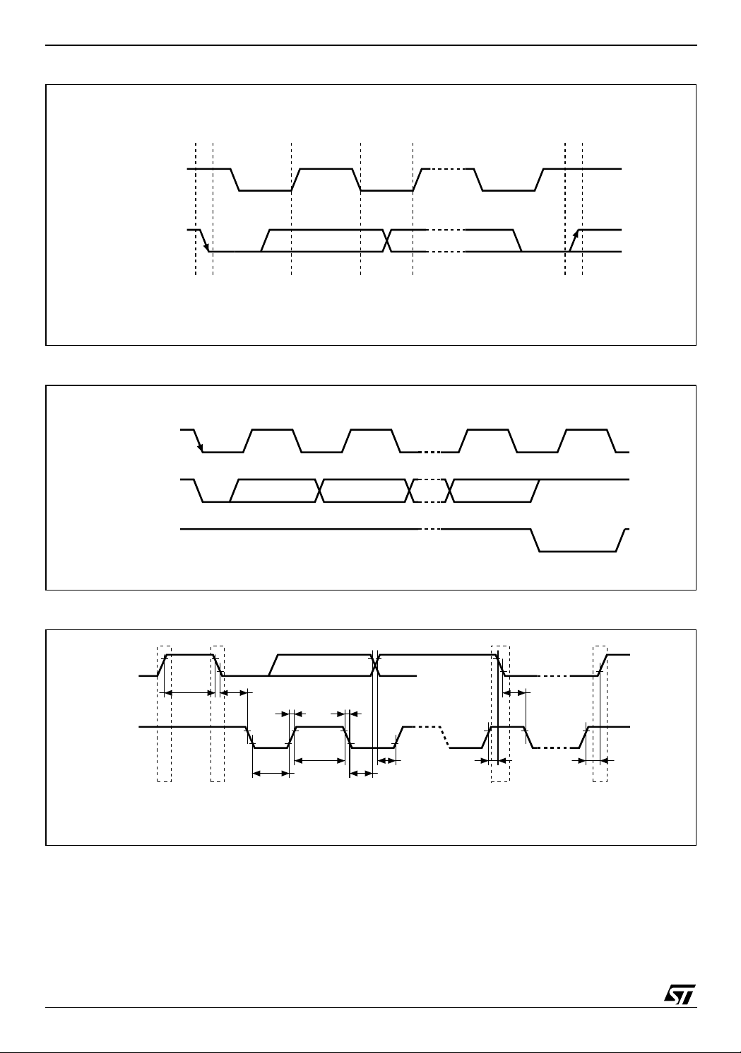
Figure 11. Bus Timing Requirements Sequence
SDA
tHD:STAtBUF
tR
SCL
SP
tF
tHIGH
tLOW
CHANGE OF
tSU:DAT
tHD:DAT
STOP
CONDITION
CLOCK PULSE FOR
ACKNOWLEDGEMENT
tHD:STA
SR
AI00587
AI00601
tSU:STOtSU:STA
P
10/31
AI00589
 Loading...