


32 Mbit (2Mb x16, Dual Bank, Page) Flash Memory
and 4 Mbit (256Kb x16) SRAM, Multiple Memory Product
FEATURES SUMMARY
■ Multiple Memory Product
– 1 bank of 32 Mbit (2Mb x16) Flash Memory
– 1 bank of 4 Mbit (256Kb x16) SRAM
■ SUPPLY VOLTAGE
–V
–V
■ ACCESS TIMES: 85ns, 100ns, 120ns
■ LOW POWER CONSUMPTION
■ ELECTRONIC SIGNATURE
= V
DDF
= 12V for Fast Program (optional)
PPF
– Manufacturer Code: 0020h
– Top Device Code, M36DR432AD: 00A0h
– Bottom Device Code, M36DR432BD: 00A1h
=1.65V to 2.2V
DDS
M36DR432AD
M36DR432BD
Figure 1. Package
FBGA
Stacked LFBGA66 (ZA)
12 x8mm
FLASH MEMORY
■ MEMORY BLOCKS
– Dual Bank Memory Array: 4 Mbit, 28 Mbit
– Parameter Blocks (Top or Bott o m location)
■ PROGRAMMING TIME
– 10µs by Word typical
– Double Word Program Option
■ ASYNCHRONOUS PAGE MODE READ
– Page Width: 4 Words
– Page Access: 35ns
– Random Access: 85ns, 100ns, 120ns
■ DUAL BANK OPERATIONS
– Read within one Bank while Program or
Erase within the other
– No delay between Read and Write operations
■ BLOCK LOCKING
– All blocks locked at Power up
– Any combination of blocks can be locked
–WPF
■ COMMON FLASH INTERFACE (CFI)
for Block Lock-Down
– 64 bit Unique Device Identifier
– 64 bit User Programmable OTP Cells
■ ERASE SUSPEND and RESUME MODES
■ 100,000 PROGRAM/ER ASE CYCL ES per
BLOCK
■ 20 YEARS DATA RETENTI ON
– Defectivity below 1ppm/year
SRAM
■ 4 Mbit (256Kb x16)
■ LOW V
■ POWER DOWN FEATURES USING TWO
DATA RETENTION: 1.0V
DDS
CHIP ENABLE INPUTS
1/52February 2003

M36DR432AD, M36DR432B D
TABLE OF CONTENTS
SUMMARY DESCRIPTION. . . . . . . . . . . . . . . . . . . . . . . . . . . . . . . . . . . . . . . . . . . . . . . . . . . . . . . . . . . 6
Figure 2. Logic Diagram . . . . . . . . . . . . . . . . . . . . . . . . . . . . . . . . . . . . . . . . . . . . . . . . . . . . . . . . . . 6
Table 1. Signal Names . . . . . . . . . . . . . . . . . . . . . . . . . . . . . . . . . . . . . . . . . . . . . . . . . . . . . . . . . . . 6
Figure 3. TFBGA Connections (Top view through package). . . . . . . . . . . . . . . . . . . . . . . . . . . . . . . 7
SIGNAL DESCRIPTIONS . . . . . . . . . . . . . . . . . . . . . . . . . . . . . . . . . . . . . . . . . . . . . . . . . . . . . . . . . . . . 8
Address Inputs (A0-A17). . . . . . . . . . . . . . . . . . . . . . . . . . . . . . . . . . . . . . . . . . . . . . . . . . . . . . . . . . 8
Address Inputs (A18-A20). . . . . . . . . . . . . . . . . . . . . . . . . . . . . . . . . . . . . . . . . . . . . . . . . . . . . . . . . 8
Data Input/Output (DQ0-DQ15). . . . . . . . . . . . . . . . . . . . . . . . . . . . . . . . . . . . . . . . . . . . . . . . . . . . . 8
Flash Chip Enable (EF). . . . . . . . . . . . . . . . . . . . . . . . . . . . . . . . . . . . . . . . . . . . . . . . . . . . . . . . . . . 8
Flash Output Enable (GF). . . . . . . . . . . . . . . . . . . . . . . . . . . . . . . . . . . . . . . . . . . . . . . . . . . . . . . . . 8
Flash Write Enable (WF). . . . . . . . . . . . . . . . . . . . . . . . . . . . . . . . . . . . . . . . . . . . . . . . . . . . . . . . . . 8
Flash Write Protect (WPF). . . . . . . . . . . . . . . . . . . . . . . . . . . . . . . . . . . . . . . . . . . . . . . . . . . . . . . . . 8
Flash Write Protect (WPF). . . . . . . . . . . . . . . . . . . . . . . . . . . . . . . . . . . . . . . . . . . . . . . . . . . . . . . . . 8
Flash Reset/Power-Down (RPF). . . . . . . . . . . . . . . . . . . . . . . . . . . . . . . . . . . . . . . . . . . . . . . . . . . . 8
VDDF Supply Voltage (1.65V to 2.2V) . . . . . . . . . . . . . . . . . . . . . . . . . . . . . . . . . . . . . . . . . . . . . . .8
V
Programming Voltage (11.4V to 12.6V). . . . . . . . . . . . . . . . . . . . . . . . . . . . . . . . . . . . . . . . . . . 8
PPF
V
Ground.. . . . . . . . . . . . . . . . . . . . . . . . . . . . . . . . . . . . . . . . . . . . . . . . . . . . . . . . . . . . . . . . . . . 8
SSF
SRAM Chip Enable (ES). . . . . . . . . . . . . . . . . . . . . . . . . . . . . . . . . . . . . . . . . . . . . . . . . . . . . . . . . . 8
SRAM Write Enable (WS). . . . . . . . . . . . . . . . . . . . . . . . . . . . . . . . . . . . . . . . . . . . . . . . . . . . . . . . . 9
SRAM Output Enable (GS).. . . . . . . . . . . . . . . . . . . . . . . . . . . . . . . . . . . . . . . . . . . . . . . . . . . . . . . . 9
SRAM Upper Byte Enable (UBS). . . . . . . . . . . . . . . . . . . . . . . . . . . . . . . . . . . . . . . . . . . . . . . . . . . . 9
SRAM Lower Byte Enable (LBS). . . . . . . . . . . . . . . . . . . . . . . . . . . . . . . . . . . . . . . . . . . . . . . . . . . . 9
VDDS Supply Voltage (1.65V to 2.2V) . . . . . . . . . . . . . . . . . . . . . . . . . . . . . . . . . . . . . . . . . . . . . . .9
FUNCTIONAL DESCRIPTION . . . . . . . . . . . . . . . . . . . . . . . . . . . . . . . . . . . . . . . . . . . . . . . . . . . . . . . 10
Figure 4. Functional Block Diagram . . . . . . . . . . . . . . . . . . . . . . . . . . . . . . . . . . . . . . . . . . . . . . . . 10
Table 2. Main Operation Modes . . . . . . . . . . . . . . . . . . . . . . . . . . . . . . . . . . . . . . . . . . . . . . . . . . . 11
FLASH MEMORY COMPONENT . . . . . . . . . . . . . . . . . . . . . . . . . . . . . . . . . . . . . . . . . . . . . . . . . . . . . 12
Table 3. Flash Bank Architecture . . . . . . . . . . . . . . . . . . . . . . . . . . . . . . . . . . . . . . . . . . . . . . . . . . 12
Figu r e 5 . Flash Secur i ty Block and Protection Reg i s te r Memo ry Map . . . . . . . . . . . . . . . . . . . . . . 13
Flash Bus Operations . . . . . . . . . . . . . . . . . . . . . . . . . . . . . . . . . . . . . . . . . . . . . . . . . . . . . . . . . . 13
Flash Read. . . . . . . . . . . . . . . . . . . . . . . . . . . . . . . . . . . . . . . . . . . . . . . . . . . . . . . . . . . . . . . . . . . . 13
Flash Write. . . . . . . . . . . . . . . . . . . . . . . . . . . . . . . . . . . . . . . . . . . . . . . . . . . . . . . . . . . . . . . . . . . . 13
Flash Output Disable. . . . . . . . . . . . . . . . . . . . . . . . . . . . . . . . . . . . . . . . . . . . . . . . . . . . . . . . . . . . 13
Flash Standby.. . . . . . . . . . . . . . . . . . . . . . . . . . . . . . . . . . . . . . . . . . . . . . . . . . . . . . . . . . . . . . . . . 1 3
Automatic Flash Standby. . . . . . . . . . . . . . . . . . . . . . . . . . . . . . . . . . . . . . . . . . . . . . . . . . . . . . . . . 1 3
Flash Power-Down.. . . . . . . . . . . . . . . . . . . . . . . . . . . . . . . . . . . . . . . . . . . . . . . . . . . . . . . . . . . . . 13
Dual Bank Operations. . . . . . . . . . . . . . . . . . . . . . . . . . . . . . . . . . . . . . . . . . . . . . . . . . . . . . . . . . . 13
Flash Command Interface. . . . . . . . . . . . . . . . . . . . . . . . . . . . . . . . . . . . . . . . . . . . . . . . . . . . . . . 13
Flash Read/Reset Command. . . . . . . . . . . . . . . . . . . . . . . . . . . . . . . . . . . . . . . . . . . . . . . . . . . . . . 14
Flash Read CFI Query Command. . . . . . . . . . . . . . . . . . . . . . . . . . . . . . . . . . . . . . . . . . . . . . . . . . 14
2/52

M36DR432AD, M36DR432BD
Auto Select Command. . . . . . . . . . . . . . . . . . . . . . . . . . . . . . . . . . . . . . . . . . . . . . . . . . . . . . . . . . . 14
Set Configuration Register Command. . . . . . . . . . . . . . . . . . . . . . . . . . . . . . . . . . . . . . . . . . . . . . .14
Program Command. . . . . . . . . . . . . . . . . . . . . . . . . . . . . . . . . . . . . . . . . . . . . . . . . . . . . . . . . . . . . 14
Double Word Program Command. . . . . . . . . . . . . . . . . . . . . . . . . . . . . . . . . . . . . . . . . . . . . . . . . . 14
Quadruple Word Program Command.. . . . . . . . . . . . . . . . . . . . . . . . . . . . . . . . . . . . . . . . . . . . . . . 14
Enter Bypass Mode Command.. . . . . . . . . . . . . . . . . . . . . . . . . . . . . . . . . . . . . . . . . . . . . . . . . . . .15
Exit Bypass Mode Command. . . . . . . . . . . . . . . . . . . . . . . . . . . . . . . . . . . . . . . . . . . . . . . . . . . . . . 15
Program in Bypass Mode Command. . . . . . . . . . . . . . . . . . . . . . . . . . . . . . . . . . . . . . . . . . . . . . . . 15
Double Word Program in Bypass Mode Command. . . . . . . . . . . . . . . . . . . . . . . . . . . . . . . . . . . . . 15
Quadruple Word Program in Bypass Mode Comman d. . . . . . . . . . . . . . . . . . . . . . . . . . . . . . . . . . 15
Block Lock Command . . . . . . . . . . . . . . . . . . . . . . . . . . . . . . . . . . . . . . . . . . . . . . . . . . . . . . . . . . . 15
Block Unlock Command . . . . . . . . . . . . . . . . . . . . . . . . . . . . . . . . . . . . . . . . . . . . . . . . . . . . . . . . . 1 5
Block Lock-Down Command. . . . . . . . . . . . . . . . . . . . . . . . . . . . . . . . . . . . . . . . . . . . . . . . . . . . . . 1 5
Block Erase Command.. . . . . . . . . . . . . . . . . . . . . . . . . . . . . . . . . . . . . . . . . . . . . . . . . . . . . . . . . . 15
Bank Erase Command. . . . . . . . . . . . . . . . . . . . . . . . . . . . . . . . . . . . . . . . . . . . . . . . . . . . . . . . . . . 16
Erase Suspend Comma nd. . . . . . . . . . . . . . . . . . . . . . . . . . . . . . . . . . . . . . . . . . . . . . . . . . . . . . . . 16
Erase Resume Command. . . . . . . . . . . . . . . . . . . . . . . . . . . . . . . . . . . . . . . . . . . . . . . . . . . . . . . . 1 6
Protection Register Program Command . . . . . . . . . . . . . . . . . . . . . . . . . . . . . . . . . . . . . . . . . . . . . 16
Table 4. Flash Commands . . . . . . . . . . . . . . . . . . . . . . . . . . . . . . . . . . . . . . . . . . . . . . . . . . . . . . . 17
Table 5. Read Electronic Signature. . . . . . . . . . . . . . . . . . . . . . . . . . . . . . . . . . . . . . . . . . . . . . . . . 18
Table 6. Flash Read Block Protection . . . . . . . . . . . . . . . . . . . . . . . . . . . . . . . . . . . . . . . . . . . . . . .18
Table 7. Configuration Register. . . . . . . . . . . . . . . . . . . . . . . . . . . . . . . . . . . . . . . . . . . . . . . . . . . . 18
Table 8. Read Protection Register . . . . . . . . . . . . . . . . . . . . . . . . . . . . . . . . . . . . . . . . . . . . . . . . . 1 9
Table 9. Program, Erase Times and Program, Erase Endurance Cycles . . . . . . . . . . . . . . . . . . . . 19
Flash Block Locking . . . . . . . . . . . . . . . . . . . . . . . . . . . . . . . . . . . . . . . . . . . . . . . . . . . . . . . . . . . 19
Reading a Block’s Lock Status . . . . . . . . . . . . . . . . . . . . . . . . . . . . . . . . . . . . . . . . . . . . . . . . . . . . 19
Locked State . . . . . . . . . . . . . . . . . . . . . . . . . . . . . . . . . . . . . . . . . . . . . . . . . . . . . . . . . . . . . . . . . . 20
Unlocked State . . . . . . . . . . . . . . . . . . . . . . . . . . . . . . . . . . . . . . . . . . . . . . . . . . . . . . . . . . . . . . . . 20
Lock-Down State. . . . . . . . . . . . . . . . . . . . . . . . . . . . . . . . . . . . . . . . . . . . . . . . . . . . . . . . . . . . . . . 20
Locking Operations During Erase Suspend . . . . . . . . . . . . . . . . . . . . . . . . . . . . . . . . . . . . . . . . . . 20
Table 10. Flash Lock Status . . . . . . . . . . . . . . . . . . . . . . . . . . . . . . . . . . . . . . . . . . . . . . . . . . . . . . 21
Flash Status Register . . . . . . . . . . . . . . . . . . . . . . . . . . . . . . . . . . . . . . . . . . . . . . . . . . . . . . . . . . 21
Data Polling Bit (DQ7). . . . . . . . . . . . . . . . . . . . . . . . . . . . . . . . . . . . . . . . . . . . . . . . . . . . . . . . . . . 21
Toggle Bit (DQ6).. . . . . . . . . . . . . . . . . . . . . . . . . . . . . . . . . . . . . . . . . . . . . . . . . . . . . . . . . . . . . . . 21
Toggle Bit (DQ2).. . . . . . . . . . . . . . . . . . . . . . . . . . . . . . . . . . . . . . . . . . . . . . . . . . . . . . . . . . . . . . . 21
Error Bit (DQ5). . . . . . . . . . . . . . . . . . . . . . . . . . . . . . . . . . . . . . . . . . . . . . . . . . . . . . . . . . . . . . . . . 22
Erase Timer Bit (DQ3). . . . . . . . . . . . . . . . . . . . . . . . . . . . . . . . . . . . . . . . . . . . . . . . . . . . . . . . . . . 22
Polling and Toggle Bits . . . . . . . . . . . . . . . . . . . . . . . . . . . . . . . . . . . . . . . . . . . . . . . . . . . . . . . . . . 22
Table 11. Polling and Toggle Bits . . . . . . . . . . . . . . . . . . . . . . . . . . . . . . . . . . . . . . . . . . . . . . . . . . 22
Table 12. Status Register Bits. . . . . . . . . . . . . . . . . . . . . . . . . . . . . . . . . . . . . . . . . . . . . . . . . . . . . 23
SRAM COMPONENT . . . . . . . . . . . . . . . . . . . . . . . . . . . . . . . . . . . . . . . . . . . . . . . . . . . . . . . . . . . . . . 2 4
SRAM Operations . . . . . . . . . . . . . . . . . . . . . . . . . . . . . . . . . . . . . . . . . . . . . . . . . . . . . . . . . . . . . 24
Read . . . . . . . . . . . . . . . . . . . . . . . . . . . . . . . . . . . . . . . . . . . . . . . . . . . . . . . . . . . . . . . . . . . . . . . . 24
Write . . . . . . . . . . . . . . . . . . . . . . . . . . . . . . . . . . . . . . . . . . . . . . . . . . . . . . . . . . . . . . . . . . . . . . . . 24
3/52

M36DR432AD, M36DR432B D
Standby/Power-Down . . . . . . . . . . . . . . . . . . . . . . . . . . . . . . . . . . . . . . . . . . . . . . . . . . . . . . . . . . . 24
Data Retention. . . . . . . . . . . . . . . . . . . . . . . . . . . . . . . . . . . . . . . . . . . . . . . . . . . . . . . . . . . . . . . . . 2 4
Output Disable. . . . . . . . . . . . . . . . . . . . . . . . . . . . . . . . . . . . . . . . . . . . . . . . . . . . . . . . . . . . . . . . . 24
MAXIMUM RATING. . . . . . . . . . . . . . . . . . . . . . . . . . . . . . . . . . . . . . . . . . . . . . . . . . . . . . . . . . . . . . . . 25
Table 13. Absolute Maximum Ratings(1) . . . . . . . . . . . . . . . . . . . . . . . . . . . . . . . . . . . . . . . . . . . . 25
DC AND AC PARAMETERS. . . . . . . . . . . . . . . . . . . . . . . . . . . . . . . . . . . . . . . . . . . . . . . . . . . . . . . . . 26
Table 14. Operating and AC Measurement Conditions. . . . . . . . . . . . . . . . . . . . . . . . . . . . . . . . . . 26
Figure 6. AC Measurement I/O Waveform . . . . . . . . . . . . . . . . . . . . . . . . . . . . . . . . . . . . . . . . . . . 26
Figure 7. AC Measurement Load Circuit . . . . . . . . . . . . . . . . . . . . . . . . . . . . . . . . . . . . . . . . . . . . . 26
Table 15. Device Capacitance . . . . . . . . . . . . . . . . . . . . . . . . . . . . . . . . . . . . . . . . . . . . . . . . . . . . . 2 6
Table 16. Flash DC Characteristics. . . . . . . . . . . . . . . . . . . . . . . . . . . . . . . . . . . . . . . . . . . . . . . . . 27
Table 17. SRAM DC Characteristics (T
Figure 8. Flash Random Read AC Waveforms . . . . . . . . . . . . . . . . . . . . . . . . . . . . . . . . . . . . . . . . 29
Figure 9. Flash Page Read AC Waveforms . . . . . . . . . . . . . . . . . . . . . . . . . . . . . . . . . . . . . . . . . . 30
Table 18. Flash Read AC Characteristics . . . . . . . . . . . . . . . . . . . . . . . . . . . . . . . . . . . . . . . . . . . . 31
Figure 10. Flash Write AC Waveforms, Write Enable Controlled . . . . . . . . . . . . . . . . . . . . . . . . . . 32
Table 19. Flash Write AC Characteristics, Write Enable Controlled . . . . . . . . . . . . . . . . . . . . . . . . 32
Figure 11. Flash Write AC Waveforms, Chip Enable Controlled. . . . . . . . . . . . . . . . . . . . . . . . . . . 33
Table 20. Flash Write AC Characteristics, Chip Enable Controlled. . . . . . . . . . . . . . . . . . . . . . . . . 33
Figure 12. Flash Reset/Power-Down AC Waveform . . . . . . . . . . . . . . . . . . . . . . . . . . . . . . . . . . . . 34
Table 21. Flash Reset/Power-Down AC Characteristics. . . . . . . . . . . . . . . . . . . . . . . . . . . . . . . . . 34
Figure 13. Flash Data Polling DQ7 AC Waveforms. . . . . . . . . . . . . . . . . . . . . . . . . . . . . . . . . . . . . 35
Figure 14. Flash Data Toggle DQ6, DQ2 AC Waveforms. . . . . . . . . . . . . . . . . . . . . . . . . . . . . . . . 36
Table 22. Flash Data Polling and Toggle Bits AC Characteristics. . . . . . . . . . . . . . . . . . . . . . . . . . 37
Figure 15. Flash Data Polling Flowchart . . . . . . . . . . . . . . . . . . . . . . . . . . . . . . . . . . . . . . . . . . . . .37
Figure 16. Flash Data Toggle Flowchart . . . . . . . . . . . . . . . . . . . . . . . . . . . . . . . . . . . . . . . . . . . . . 37
Figure 17. SRAM Read Mode AC Waveforms, Address Controlled with UBS = LBS = V
Figure 18. SRAM Read AC Waveforms, ES or GS Controlled . . . . . . . . . . . . . . . . . . . . . . . . . . . .38
Figure 19. SRAM Standby AC Waveforms . . . . . . . . . . . . . . . . . . . . . . . . . . . . . . . . . . . . . . . . . . . 39
Table 23. SRAM Read AC Characteristics) . . . . . . . . . . . . . . . . . . . . . . . . . . . . . . . . . . . . . . . . . . . 39
Figure 20. SRAM Write AC Waveforms, WS Controlled with GS Low . . . . . . . . . . . . . . . . . . . . . .40
Figure 21. SRAM Write AC Waveforms, WS Controlled with GS High. . . . . . . . . . . . . . . . . . . . . . 40
Figure 22. SRAM Write Cycle Waveform, UBS and LBS Controlled, G Low . . . . . . . . . . . . . . . . .41
Figure 23. SRAM Write AC Waveforms, ES Controlled . . . . . . . . . . . . . . . . . . . . . . . . . . . . . . . . .41
Table 24. SRAM Write AC Characteristics . . . . . . . . . . . . . . . . . . . . . . . . . . . . . . . . . . . . . . . . . . . 42
Figure 24. SRAM Low V
Table 25. SRAM Low V
Data Retention AC Waveforms, ES Controlled . . . . . . . . . . . . . . . . . 42
DDS
Data Retention Characteristics (1, 2) . . . . . . . . . . . . . . . . . . . . . . . . . 43
DDS
= –40 to 85°C; V
A
DDF
= V
= 1.65V to 2.2V) . . . . . . . . 28
DDS
. . . . . . 38
IL
PACKAGE MECHANICAL . . . . . . . . . . . . . . . . . . . . . . . . . . . . . . . . . . . . . . . . . . . . . . . . . . . . . . . . . . 44
Figure 25. Stacked LFBGA 12x8mm - 8x8 ball array, 0.8mm pitch, Bottom View Package Outline44
Table 26. Stacked LFBGA 12x8mm - 8x8 ball array, 0.8mm pitch, Package Mechanica l Data . . . 44
4/52

M36DR432AD, M36DR432BD
PART NUMBERING . . . . . . . . . . . . . . . . . . . . . . . . . . . . . . . . . . . . . . . . . . . . . . . . . . . . . . . . . . . . . . . 45
Table 27. Ordering Information Scheme . . . . . . . . . . . . . . . . . . . . . . . . . . . . . . . . . . . . . . . . . . . . . 45
APPENDIX A. BLOCK ADDRESSES. . . . . . . . . . . . . . . . . . . . . . . . . . . . . . . . . . . . . . . . . . . . . . . . . . 46
Table 28. Bank A, Top Boot Block Addresses M36DR432AD . . . . . . . . . . . . . . . . . . . . . . . . . . . . 46
Table 29. Bank B, Top Boot Block Addresses M36DR432AD . . . . . . . . . . . . . . . . . . . . . . . . . . . . 46
Table 30. Bank B, Bottom Boot Block Addresses M36DR432BD . . . . . . . . . . . . . . . . . . . . . . . . . . 47
Table 31. Bank A, Bottom Boot Block Addresses M36DR432BD . . . . . . . . . . . . . . . . . . . . . . . . . . 47
APPENDIX B. COMMON FLASH INTERFACE . . . . . . . . . . . . . . . . . . . . . . . . . . . . . . . . . . . . . . . . . . 48
Table 32. Query Structure Overview . . . . . . . . . . . . . . . . . . . . . . . . . . . . . . . . . . . . . . . . . . . . . . . .48
Table 33. CFI Query Identification String . . . . . . . . . . . . . . . . . . . . . . . . . . . . . . . . . . . . . . . . . . . .48
Table 34. CFI Query System Interface Information. . . . . . . . . . . . . . . . . . . . . . . . . . . . . . . . . . . . . 49
Table 35. Device Geometry Definition. . . . . . . . . . . . . . . . . . . . . . . . . . . . . . . . . . . . . . . . . . . . . . .50
REVISION HISTORY. . . . . . . . . . . . . . . . . . . . . . . . . . . . . . . . . . . . . . . . . . . . . . . . . . . . . . . . . . . . . . . 51
Table 36. Document Revision History. . . . . . . . . . . . . . . . . . . . . . . . . . . . . . . . . . . . . . . . . . . . . . .51
5/52
M36DR432AD, M36DR432B D
SUMMARY DESCRIPTION
The M36DR432AD/BD is a low-voltage Multiple
Memory Product which combines two memory devices: a 32 Mbit (2Mbit x16) non-volatile Flash
memory and a 4 Mbit SRAM.
The memory is available in a Stacked LFBGA66
12x8mm - 8x8 active ball array, 0.8mm pitch package and supplied with all the bits erased (set to
‘1’).
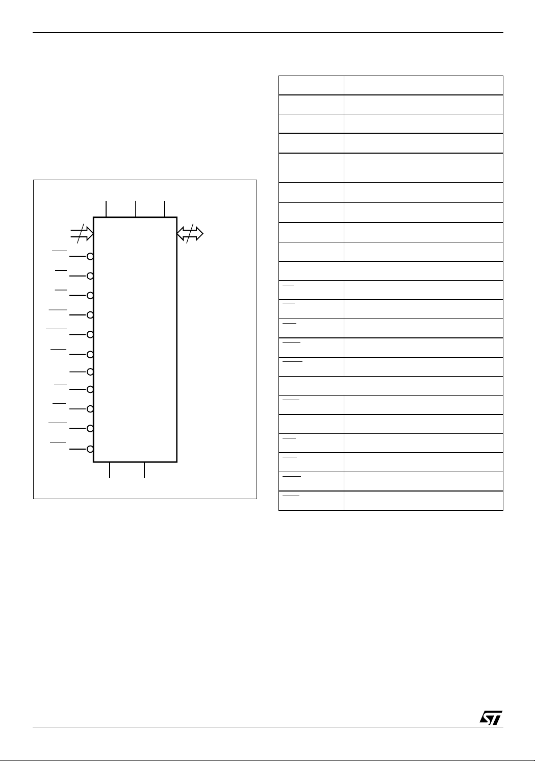
Figure 2. Logic Diagram
Table 1. Signal Names
A0-A17 Address Inputs
A18-A20 Address Inputs for Flash Chip only
DQ0-DQ15 Data Input/Outputs, Command Inputs
V
V
DDF
PPF
Flash Power Supply
Flash Optional Supply V oltage for Fast
Program & Erase
A0-A20
WF
EF
GF
RPF
WPF
E1S
E2S
GS
WS
UBS
LBS
21
V
V
DDF
PPF
M36DR432AD
M36DR432BD
V
SSF
V
SSS
V
DDS
16
DQ0-DQ15
AI07309b
V
SSF
V
DDS
V
SSS
NC Not Connected Internally
Flash control functions
EF
GF
WF
RPF
WPF
SRAM control functions
1S Chip Enable
E
E2S Chip Enable
GS
WS
UBS
LBS
Flash Ground
SRAM Power Supply
SRAM Ground
Chip Enable
Output Enable
Write Enable
Reset/Power-Down
Write Protect input
Output Enable
Write Enable
Upper Byte Enable
Lower Byte Enable
6/52
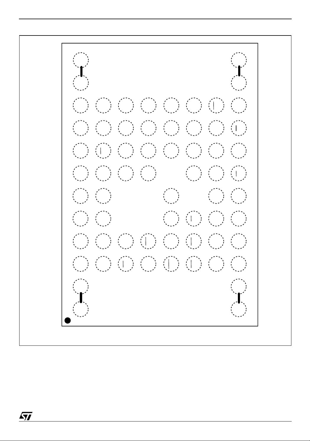
Figure 3. TFBGA Connections (Top view through package)
#4#3
NCNC
M36DR432AD, M36DR432BD
AI90204
NC
NCNCGF
87654321
NC
SSF
V
A12
A13A11A20NCNC
A15 A14
DQ7
DQ14
WS
DQ15A9A16
A8 A10
DQ5
DQ4
DQ6DQ13NCWF
DDF
V
DDS
V
E2SDQ12V
RPF
SSS
DQ3DQ2
DQ10
DQ11A19WPF
PPF
V
DQ1DQ0
DQ8DQ9GSLBS
UBS
E1SA1
A2A3A6A7A18
A17
SSF
EFA0A4NCNC
A5
NC V
#2#1
A
B
C
D
E
F
G
H
7/52

M36DR432AD, M36DR432B D
SIGNAL DESCRIPTIONS
See Figure 2 Logic Diagram and Tabl e 1, Signal
Names, for a brief overview of the signals connected to this device.
Address Inputs (A0-A17). Addresses A0-A17 are common inputs for the Flash an d the SRAM components. The Address Inputs select the cells in the memory array to access during Bu s Read operations. During Bus Write operations they control the commands sent to the Command Interface of the internal state machine. During a write operation, the address inputs for the Flash memory are latched on the falling edge of the Flash Chip E nable (EF last, whereas for the SRAM array they are latched on the falling edge of the SRAM Chip Enable lines (E1S the datasheet, only the Active Low SRAM Chip Enable line will be di scussed. I t wil l be ref erred to as ES
Address Inputs (A18-A20). Addresses A18-A20 are inputs for the Flash component only. They are latched during a write operation on the falling edge of Flash Chip Enable (EF whichever occurs last.
Data Input/Output (DQ0-DQ15). The Data I/O output the data stored at the selected address during a Bus Read operation or input a command or the data to be programmed during a Write Bus operation.
The input is data to be programmed in the Flash or
SRAM memory array or a command to be written
to the C.I. of the Flash memory. Both are latched
on the rising edge of Flash Write Enable (WF
SRAM Chip Enable lines (ES
(WS
array or SRAM array, the Electronic Signature
Manufacturer or Device codes, the Block Protection status, the Configuration Register status or
the Status Register Data (Polling bit DQ7, Toggle
bits DQ6 and DQ2, Error bit DQ5 or Erase Timer
bit DQ3) depending on the address. Outputs are
valid when Flash Chip Enable (EF
able (GF
Output Enable (GS
The output is high impedance when both the Flash
chip and the SRAM chip are deselected or the outputs are disabled and when Reset (RPF
Flash Chip Enable (EF
activates the Flash memory control logic, input
buffers, decoders and sense amplifiers. When
Chip Enable is at V
and the power consumption is reduced to the
standby level.
Flash Output Enable (GF
through the data buffers during a read operation.
) or Write Enable (WF), whichever occurs
or E2S) or Write Enable (WS). In the rest of
.
) or Write Enable (WF),
) and,
) or Write Enable
). The output is data from the Flash memory
) and Output En-
) or SRAM Chip Enable lines (ES) and
) are active.
) is at VIL.
). The Chip Enable input
the memory is deselected
IH
). gates the outputs
When Output Enable, GF
, is at VIH the outputs are
High impedance.
Flash Write Enable (
WF). The Write Enable
controls the Bus Write operation of the Flash
memory’s Command Interface.
Flash Write Protect (WPF
). Write Protect is an
input that gives an additional hardware protect ion
for each Flash block. When Write Protect is at V
IL
the locked-down blocks cannot be locked or unlocked. When Write Protect is at V
, the Lock-
IH
Down is disabled and the Locked-Down blocks
can be locked or unlocked. Refer to Table 8, Read
Protection Register.
Flash Reset/Power-Down (RPF
). The Reset/
Power-Down input provides hardwa re res et of the
Flash memory, and/or Power-Down functions, depending on the Flash Configuration Register status. Reset or Power-Down of the memory is
achieved b y pulling RPF
to VIL for at least t
PLPH
.
The Reset/Power-Down function is set in the Configuration Register (see Set Configuration Register Command). If it is set to ‘0’ the Reset function
is enabled, if it is set to ‘1’ the Power-Down function is enabled. After a Reset or Power-Up the
power save function is disabled and all blocks are
locked.
The memory Command Interface is reset on Power Up to Read Array. Either Chip Enabl e or Write
Enable must be tied to V
during Power Up to al-
IH
low maximum security and the possibility to write a
command on the first rising edge of Write Enable.
After a Reset, when the de vice is in Re ad, Eras e
Suspend Read or Standby, valid data will be output t
PHQ7V1
after the rising edge of RPF. If the device is in Erase or Program, the operation will be
aborted and the reset recovery will t ake a maximum of t
set/Power-Down t
RPF
. See Tables 18 and 19, and Figure 12.
Supply Voltage (1.65V to 2.2 V). V
V
DDF
. The memory will recover from Re-
PLQ7V
PHQ7V2
after the rising ed ge of
DDF
provides the power supply to the internal core and I/O
pins of the memory device. It is the main power
supply for all operations (read, program and
erase).
Programming Voltage (11.4V to 12.6V).
V
PPF
provides a high voltage power supply for fast
V
PPF
factory programming. V
is required to use the
PPF
Double Word and Quadruple Word Program commands.
V
Ground. V
SSF
ground is the reference for
SSF
the core supply. It must be connected to the system ground.
SRAM Chip Enable (ES
). The Chip Enable in-
puts for SRAM activate the memory con trol logic,
input buffers and decoders. ES
at VIH deselects
,
8/52

M36DR432AD, M36DR432BD
the memory and red uces the power consumption
to the standby level. ES
can also be used to control writing to the SRAM memory array, while WS
remains at VIL. It is not allowed to set EF at VIL and
ES
at VIL at the same time.
SRAM Write Enable (WS
). The Write Enable in-
put controls writing to the SRAM memory array.
WS
is active Low.
SRAM Output E nable (GS
). The Output Enable
gates the outputs through the data buffers during
a read operation of the SRAM c hip. GS
is active
Low.
SRAM Upper Byte Enable (UBS
upper bytes for SRAM (DQ8-DQ15). UBS
). Enables the
is acti ve
Low.
SRAM Lower Byte Enable (LBS
lower bytes for SRAM (DQ0-DQ7). LBS
). Enables the
is active
Low.
V
Supply Voltage (1.65V to 2.2V) . V
DDS
DDS
is the
SRAM power supply for all operations.
Note: Each device in a system should have
V
DDF
and V
decoupled with a 0.1µF capaci-
PPF
tor close to the pin. See Figure 7, AC Measurement Load Circuit. The PCB trace widths
should be sufficient to carry the required V
PPF
program and erase currents.
9/52
M36DR432AD, M36DR432B D
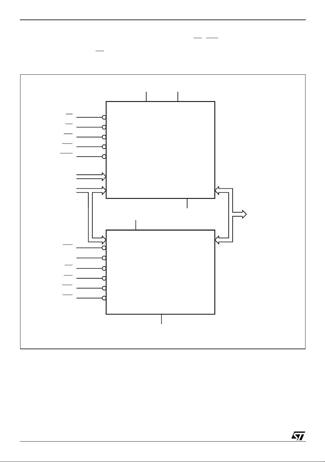
FUNCTIONAL DESCRIPTION
The Flash and SRAM components have separate
power supplies and grounds and are distinguished
by three chip enable inputs: EF
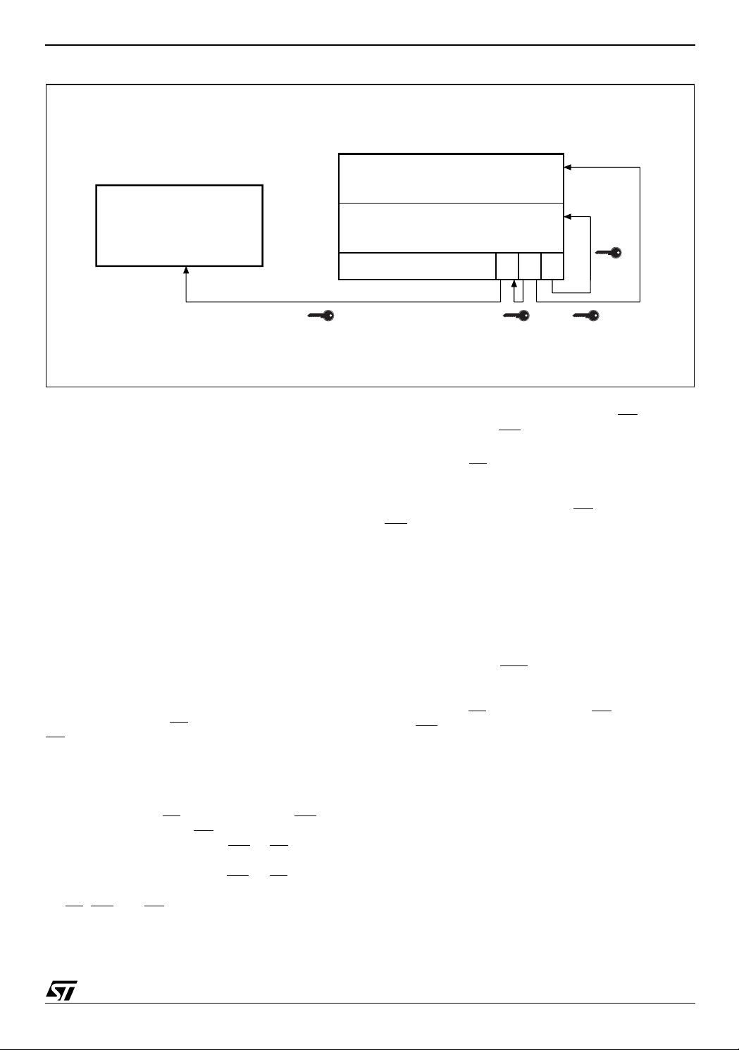
Figure 4. Funct i on a l Bl ock D i agram
for the Flash mem-
ory and ES
SRAM .
(E1S and E2S, respectively) f or the
EF
GF
WF
RPF
WPF
A18-A20
A0-A17
E1S
E2S
GS
WS
UBS
LBS
V
DDF
Flash Memory
32 Mbit (2Mb x 16)
V
DDS
SRAM
4 Mbit (256Kb x 16)
V
PPF
V
SSF
DQ0-DQ15
10/52
V
SSS
AI07310b
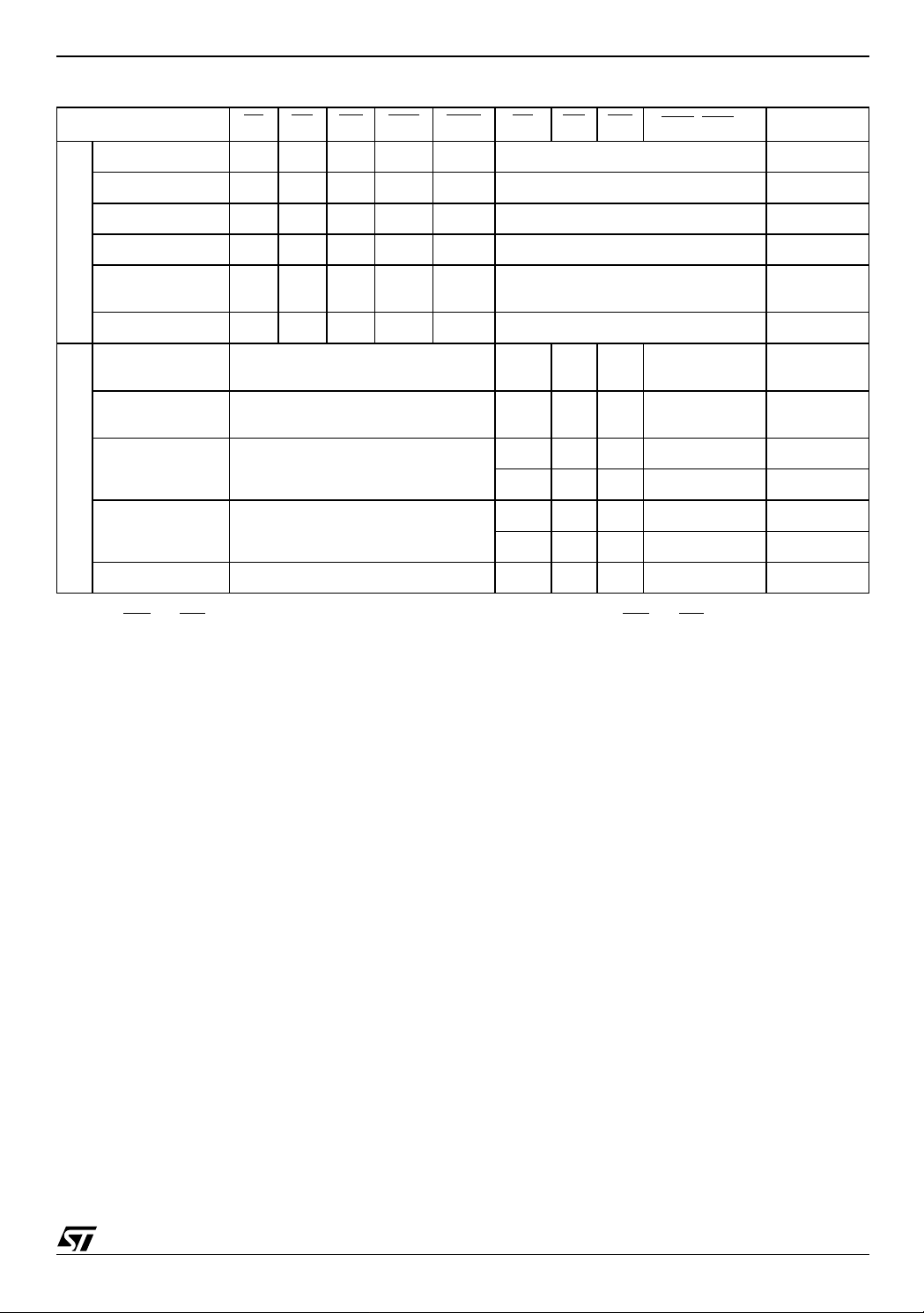
Table 2. Main Operation Modes
Operation Mode EF GF WF RPF WPF ES GS WS
V
V
Read
Page Read
Write
Standby
Reset/
Flash Memory
Power-Down
Output Disable
IL
V
IL
V
IL
V
IH
XXX
V
IL
V
IL
V
V
IL
V
IH
XX
V
V
IH
Read Flash must be disabled
V
IH
V
IH
V
V
IL
V
V
V
IH
V
IH
IH
IH
IH
IL
IH
IH
V
IH
V
IH
V
IH
V
IH
V
IH
SRAM must be disabled Data Output
SRAM must be disabled Data Output
SRAM must be disabled Data Input
Any SRAM mode is allowed Hi-Z
Any SRAM mode is allowed Hi-Z
Any SRAM mode is allowed Hi-Z
V
VILV
IL
M36DR432AD, M36DR432BD
(1)
DQ15-DQ0
Data out
Word Read
IH
UBS, LBS
V
IL
Write Flash must be disabled
Standby/Power
Down
SRAM
Any Flash mode is allowable
Data Retention Any Flash mode is allowable
Output Disable Any Flash mode is allowable
Note: 1. X = Don’t care (VIL or VIH).
UBS and LBS are tied toge ther the bus is at 16 bit. For an 8 bi t bus configuration use U BS and LBS separately.
2. If
V
V
IL
IHVIL
V
X X X Hi-Z
IH
XXX
V
X X X Hi-Z
IH
XXX
V
V
IL
IHVIH
V
IL
V
IH
V
IH
Data in Word
Write
Hi-Z
Hi-Z
X Hi-Z
11/52

M36DR432AD, M36DR432B D
FLASH MEMORY COMPONENT
The Flash Memory is a 32 Mbit (2Mbit x16) nonvolatile Flash memory that may be erased electrically at block level and programmed in-s ystem on
a Word-by-Word basis using a 1.65V to 2.2V V
supply for the circuitry and a 1.65V to 2.2V V
supply for the Input/Output pins (in the stacked device , V
tional 12V V
DDF
and V
power supply is provided to speed
PPF
are tied internally). An op-
DDQF
up customer programming.
The Flash device features an asymmetrical block
architecture with an array of 71 bl ocks divided into
two banks, Banks A and B, providing Dual Bank
operations. While programming or erasing in Bank
A, read operations are poss ible in Ban k B or vice
versa. Only one ban k at a t ime is allowed to be in
program or erase mode. The ba nk architectu re is
summarized in Table 3, and the B lock Addresses
are shown in Appendi x A. The Parameter B locks
are located at the top of the memory address
space for the M36DR432AD and, at the bottom for
the M 36DR432BD.
Each block can be erased separately. Erase can
be suspended, in order to perform either read or
program in any other block, and then resumed.
Each block can be programmed and erased over
100,000 cycles.
DDF
DDQF
Program and Erase command s are written to the
Command Interface of the memory. An internal
Program/Erase Controller takes care of the timings necessary for program and erase operations.
The end of a program or erase operation can be
detected and any error conditions identified in the
Status Register. The command set required to
control the memory is consistent with JEDEC standards.
The Flash memory features an instant, individual
block locking scheme that allo ws any block to be
locked or unlocked with no latency, enabling instant code and data protection. All blocks have two
levels of protection. They can be individually
locked and locked-down preventing any accidental programming or erasure. All blocks are locked
at Power Up and Reset.
The device includes a 128 b it Protection Register
and a Security Block to increase the protection of
a system’s design. The Prote ction Register is divided into two 64 bit segments. The first segment
contains a unique device numb er written by ST,
while the second one is one-time-programmable
by the user. The user programmable segment can
be permanently protected. The Security Block, parameter block 0, can be permanently protected by
the user. Figure 5, shows the Flash Security Block
and Protection Register Memory Map.
Table 3. Flash Bank Architecture
Bank A 4 Mbits 8 blocks of 4 KWords 7 blocks of 32 KWords
Bank B 28 Mbits - 56 blocks of 32 KWords
Bank Size Parameter Blocks Main Blocks
12/52
M36DR432AD, M36DR432BD
Figure 5. Flash Security Block and Protection Register Memo ry Ma p
PROTECTION REGISTER
88h
SECURITY BLOCK
85h
84h
Parameter Block # 0
81h
80h
User Programmable OTP
Unique device number
Protection Register Lock 2 1 0
AI06185
Flash Bus Operations
The following operations can be performed using
the appropriate bus cycles: Flash Read Array
(Random and Page Modes), Flash Write, Flash
Output Disable, Flash Standby and F lash Reset/
Power-Down, see Table 2, Main Operation
Modes.
Flash Read. Flash Read operat ions are used to output the contents of the Memory Array, the Electronic Signature, the Status Register, the CF I, the Block Protection Status or the Configuration Register status. Read operation of the Flash memory array is performed in asynchronous page mode, that provides fast access time. Data is internally read and stored in a page buffer. The page has a size of 4 words and is addressed by A0-A1 address inputs. Read operations of the Electronic Signature, the Status Register, the CFI, the Block Protection Status, the Configuration Register status and the Security Code are performed as single asynchronous read cycles (Random Read). Both Flash Chip Enable EF GF
must be at VIL in order to read the output of the
and Flash Output Enable
memory. Flash Write. Write operations are used to give
commands to the memory or to latch Input Data to
be programmed. A write operation is initiated
when Chip Enable EF
with Output E nable G F at VIH. Addresses are
V
IL
latched on the falling edge of WF
and Write Enable WF are at
or EF whichever
occurs last. Commands and Input Data are
latched on the rising edge of WF
or EF whichever
occurs first. Noise pulses of less than 5ns typical
on EF
, WF and GF signals do not start a write cy-
cle.
Flash Output Disable. The data outputs are high impedance when the Output Enable GF
is at V
IH
with Write Enable WF at VIH. Flash Standby. The memory is in standby when
Chip Enable EF
is at VIH and the P/E.C. is idle.
The power consumption is reduced to the standby
level and the outputs are high imped ance, independent of the Output Enable GF
inputs.
WF
or Write Enable
Automatic Flash Standby. In Read mode, after 150ns of bus inactivity and when CMOS levels are driving the addresses, the chip automatically enters a pseudo-standby mode where consumption is reduced to the CMOS standby value, while outputs still drive the bus.
Flash Power-Down. The memory is in PowerDown when the Configuration Register is set for/ Power-Down and RPF
is at VIL. The power consumption is reduced to the Power-Down level, and
Outputs are high impedance, independent of the
Chip Enable EF
able WF
inputs.
, Output Enable GF or Write En-
Dual Bank Operations. The Dual Bank allows data to be read from on e bank of memory while a program or erase operation is i n progress in the other bank of the memory. Read and Write cycles can be initiated for simultaneous operations in different banks without any delay. Status Register during Program or Erase must be monitored using an address within the bank being modified.
Flash Command Interface
All Bus Write operations t o the me mory are in terpreted by the Command Interface. Commands
consist of one or more sequential Bus Write operations. An internal Program/Erase Controller han-
13/52

M36DR432AD, M36DR432B D
dles all timings and verifies the correct execution
of the Program and Erase commands. Two bus
write cycles are required to unlo ck the Com mand
Interface. They are followed by a setup or confirm
cycle. The increased number of write cycles is to
ensure maximum data security.
The Program/Erase Controller provides a Status
Register whose output may be read at any time to
monitor the progress or the result of the operation.
The Command Interface is reset to Read mode
when power is first applied or exiting from Reset.
Command sequences must be followed exactly.
Any invalid combination of commands will reset
the device to Read mode
Flash Read/Reset Command. The Read/Reset command returns the device to Read mode. One Bus Write cycle is required to issue the Read/Reset command and return the device to Read mode. Subsequent Read operations will read the addressed location and output the data. The write cycle can be preceded by the unlock cycles but it is not mandatory.
Flash Read CFI Query Command. The Read CFI Query command is used to read data from the Common Flash Interface (CFI) and the Electronic Signature (Manufacturer or the Device Code, see Table 5). The Read CFI Query Command consists of one Bus Write cycle. Once the command is issued the device enters Read CFI mode. Subsequent Bus Read operations read the Common Flash Interface or Electronic Signature. Once the device has entered Read CFI mode, only the Read/Reset command should be used and no other. Issuing the Read/Res et command returns t he device to Read mode.
See Appendix B, Common Flash Interface, Tables
33, 34, and 35 for details on the information contained in the Common Flash Interface memory area.
Auto Select Command. The Auto Select command uses the two unlock cycles followed by one write cycle to any bank address to setup the command. Subsequent reads at any address will ou tput the Block Protection status, Protection Register and Protection Register Lock or the Configuration Register status depending on the levels of A0 and A1 (see Tables 6, 7 an d 8). Once the Auto Select command has been issued only the Read/Reset command should be used and no other. Issuing the Read/Res et command returns t he device to Read mode.
Set Conf iguration Regist er Command . The Flash component contains a Configuration Register, see Table 7, Configuration Register.
It is used to define the status of the Res et/PowerDown functions. The value for the Configuration
Register is always presented on A0-A15, the other
address bits are ignore d. Address input A10 defines the status of the Reset/Power-Down func-
tions. If it is set to ‘0’ the Reset function is enabled,
if it is set to ‘1’ the Power-Down function is enabled. At Power Up the Configuration Register bit
is set to ‘0’.
The Set Configuration Register command is used
to write a new value to the Configuration Register.
The command uses the two unlock cycles followed
by one write cycle to setup the command and a
further write cycle to wri te the data and confirm the
command.
Program Command. The Program command uses the two unlock cycles followed by a write cycle to setup the command and a further write cycle to latch the Address and Dat a and start the Program Erase Controller. Read operations within the same bank output the Status Register after programming has started.
Note that the Program command cannot change a
bit set at ’0’ bac k to ’1’. One of the E rase Commands must be used to set all the bits in a block or
in the whole bank from ’0’ to ’1’. If the Program
command is used to try to set a bi t from ‘0’ to ‘ 1’
Status Register Error bit DQ5 will be set to ‘1’, only
is in the range of 11.4V to 12.6V.
if V
PPF
Double Word Pr ogr a m C omman d. This feature is offered to improve the programming throughput by writing a page of two adjacent words in parallel. The V
supply voltage is required to be from
PPF
11.4V to 12.6V for the Double Word Program command.
The command uses the two unlock cycles followed
by a write cycle to setup the command. A further
two cycles are required t o latch the address and
data of the two Words and start the Program Erase
Controller.
The addresses must be the same except for the
A0. The Double Wo rd Program com mand can be
executed in Bypass mode t o skip the two unlock
cycles.
Note that the Double Word Program command
cannot change a bit set at ’0’ back to ’1’. One of the
Erase Commands must be used to set all the bits
in a block or in the whole bank from ’0’ to ’1’. If the
Double Word Program comm and is used t o try to
set a bit from ‘0’ to ‘1’ Status Register Error bit DQ5
will be set to ‘1 ’.
Quadruple Word Program Command. The Quadruple Word Program command improves the programming throughput by writing a page of four adjacent words in parallel. The four words must differ only for the addresses A0 and A1. The V
PPF
supply voltage is required to be from 11.4V to
12.6V for the Quadruple Word Program command.
14/52

M36DR432AD, M36DR432BD
The command uses the two unlock cycles followed
by a write cycle to setup the command. A further
four cycles are required to latch the address and
data of the four Words and start the Program
Erase Controller.
The Quadruple Word Program command can be
executed in Bypass mode t o skip the two unlock
cycles.
Note that the Quadruple Word Program command
cannot change a bit set to ’0’ back to ’1’. One of the
Erase Commands must be used to set all the bits
in a block or in the whole bank from ’0’ to ’1’. If the
Quadruple Word Program command is used to try
to set a bit from ‘0’ to ‘ 1’ Status Register E rror bit
DQ5 will be set to ‘1’.
Enter Bypas s Mode Comman d. The Bypass mode is used to reduce the overall programming time when large memory array s need to be programmed.
The Enter Bypass Mode command uses the two
unlock cycl e s followed by on e wri te cycle to set u p
the command. Once in Bypass mode, it is imperative that only the following commands be issued:
Exit Bypass, Program, Double Word Program or
Quadruple Word Program.
Exit Bypass Mode Command. The Exit Bypas s Mode command uses two write cycles to setup and confirm the command. The unlock cycles are not required. After the Exit Bypass Mode command, the device resets to Read mode.
Program in Bypass Mode Command. The Program in Bypass Mode command can be issued when the device is in Bypas s m ode (issue a Enter Bypass Mode command). It uses the same sequence of cycles as the Program command with the exception of the unlock cycles.
Double Word Program in Bypass Mode Command. The Double Word Program in Bypass
Mode command can be issued when the device is
in Bypass mode (issue a Enter Bypass Mode command). It uses the same sequence of cycles as the
Double Word Program comma nd with the exception of the unlock cycles.
Quadruple Word Program in Bypass Mode Command. The Quadruple Word Program in By-
pass Mode command can be issued when the device is in Bypass mode (issue a Enter Bypass
Mode command). I t uses the same sequence of
cycles as the Quadruple Word Program command
with the exception of the unlock cycles.
Block Lock Command. The Block Lock command is used to lock a block and prevent Program
or Erase operations from changing the data i n it.
All blocks are locked at power-up or reset.
Three Bus Write cycles are required to issue the
Block Lock command.
■ The first two bus cycles unlock the Command
Interface.
■ The third bus cycle sets up the Block Lock
command and latches the block address.
The lock status can be monitored for each block
using the Auto Select comma nd. Table 10 shows
the Lock Status a fter issuing a Block Lock command.
The Block Lock bits are vo latile, once set they remain set until a hardware reset or power-down/
power-up. They are cleared by a Blocks Unlock
command. Refer to the section, Block Locking, for
a detailed explanation.
Block Unlock Command. The Blocks Unlock
command is used to unlock a block, allowing the
block to be programmed or erased.
Three Bus Write cycles are required to issue the
Blocks Unlock command.
■ The first two bus cycles unlock the Command
Interface.
■ The third bus cycle sets up the Block UnLock
command and latches the block address.
The lock status can be monitored for each block
using the Auto Select comma nd. Table 10 shows
the lock status after issuing a Block Unlock command. Refer to the section, Block Locking, for a
detailed explanation.
Block Lock-Down Command. A locked or unlocked block can be locked-down by issuing the
Block Lock-Down command. A locked-down block
cannot be programmed or erased, or have its protection status changed when WPF
When WPF
is High, V
the Lock-Down function is
IH,
is Low, VIL.
disabled and the locked blocks can be individually
unlocked by the Block Unlock command.
Three Bus Write cycles are required to issue the
Block Lock-Down command.
■ The first two bus cycles unlock the Command
Interface.
■ The third bus cycle sets up the Block Lock-
Down command and latches the block address.
The lock status can be monitored for each block
using the Auto Select command. Locked-Down
blocks revert to the locked (and not locked-down)
state when the device is reset on power-down. Table 10 shows the Lock Status after issuing a Block
Lock-Down command. Refer to the section, Block
Locking, for a detailed explanation.
Block Erase Command. The Block Erase command can be used to erase a bloc k. It set s all t he bits within the selected block to ’1’. All previous data in the block is lost. If the block is protected then the Erase operation will abort, the data in the block will not be changed and the device will return to Read Array mode. It is not necessary to pre-pro-
15/52

M36DR432AD, M36DR432B D
gram the block as the Program/ Erase Controller
does it automatically before erasing.
Six Bus Write cycles are required to issue the
command.
■ The first two write cycles unlock the Command
Interface.
■ The third write cycles sets up the command
■ the fourth and fifth write cycles repeat the unlock
sequence
■ the sixth write cycle latches the block address
and confirms the command.
Additional Block Erase confirm cycles can be issued to erase other bloc ks without further unlock
cycles. All blocks must belong to the same bank; if
a new block belonging to the other ban k is given,
the operation is aborted.
The additional Block Erase confirm cycles must be
given within the DQ3 erase timeout period. Each
time a new confirm cycle is issued the timeout period restarts. The status of the internal timer can
be monitored through the level of DQ3, see Status
Register section for more details.
Once the command is issued the device outputs
the Status Register data when any address within
the bank is read.
After the command has been issued the Flash
Read/Reset command will be accepted during the
DQ3 timeout period, after that only the Erase Suspend command will be accepted.
On successfu l compl etio n of t he Bl ock Erase c ommand, the device returns to Read Array mode.
Bank Erase Command. The Bank Erase command can be used to eras e a bank. It sets all the
bits within the selected bank to ’1’. All previous
data in the bank is lost. The Bank Erase command
will ignore an y pro tec t e d b locks within the bank. If
all blocks in the bank are protected then the Bank
Erase operation will abort and the data in the bank
will not be changed. It is not necessary to pre-program the bank as the Program/Erase Controller
does it automatically before erasing.
As for the Block Erase command six Bus Write cycles are required to issue the command.
■ The first two write cycles unlock the Command
Interface.
■ The third write cycles sets up the command
■ the fourth and fifth write cycles repeat the unlock
sequence
■ the sixth write cycle latches the block address
and confirms the command.
Once the command is issued the device outputs
the Status Register data when any address within
the bank is read.
On successful completion of the Bank Erase command, the device returns to Read Array mode.
Erase Suspend Command. The Erase Suspend command is used to pause a Block Erase operation. In a Dual Bank memory it can be used to read data within the bank where an Erase operation is in progress. It is also possible to program data in blocks not being erased.
One bus write cycle is required to issue the Erase
Suspend command. The Program/Erase Controller suspends the Erase operation within 20µs of
the Erase Suspend command being issued and
bits 7, 6 and/ or 2 of the Status Register are set to
‘1’. The device is then automatically set to Read
mode. The command can be addressed to any
bank.
During Erase Suspend the memory will accept the
Erase Resume, Program, Read CFI Query, Auto
Select, Block Lock, Block U nlock and B lo ck Lo ckDown commands.
Erase Resume Command. The Erase Resume command can be used to restart the Program/ Erase Controller after an Erase Suspend command has paused it. One Bus Write cycle is required to issue the command. The command must be issued to an address within the bank being erased. The unlock cycles are not required.
Protection R egister Progr am C om m and. The
Protection Register Program c omm and is used to
Program the Protection Register (One-Time-Programmable (OTP) segment and Protection Register Lock). The OTP segment is programmed 16
bits at a time. When shipped all bits in the segment
are set to ‘1’. The user can only program the bits
to ‘0’ .
Four write cycles are required to issue the Protection Register Program command.
■ The first two bus cycles unlock the Command
Interface.
■ The third bus cycle sets up the Protection
Register Program command.
■ The fourth latches the Address and the Data to
be written to the Protection Register and starts
the Program/Erase Controller.
Read operations output the Status Register content after the programming has started.
The OTP segment can be p rotected by programming bit 1 of the Protection Register Lock. The
segment can be protected by programming bit 1 of
the Protection Register Lock. Bit 1 of the P rotection Register Lock also protects bit 2 of the Protection Register Lock. Programming bit 2 of the
Protection Register Lock will result in a permanent
protection of Parameter Block #0 (see Figure 5,
Flash Security Block and Protection Register
Memory Map). Attempting to program a previously
16/52
 Loading...