


32 Mbit (2Mb x16, Dual Bank, Page) Flash Memory
and 2 Mbit (128K x16) SRAM, Multiple Memory Product
FEATURES SUMMARY
■ SUPPLY VOLTAGE
–V
DDF=VDDS
–V
■ ACCE SS TIME: 100,120ns
■ LOW POWE R CONSUMPT ION
■ ELECTRONIC SIGNATURE
= 12V for Fast Program (optional)
PPF
– Manufacturer Code: 20h
– Top Device Code, M36DR232A: 00A0h
– Bottom Device Code, M36DR232B: 00A1h
FLASH MEMORY
■ 32 Mbit (2Mb x16) BOOT BLOCK
– Parameter Blocks (Top or Bottom Location)
■ PROGRAMMING TIME
– 10µs typical
– Double Word Programming Option
■ ASYNCRONOUS PAGE MODE READ
– Page width: 4 Word
– Page Mode Access Time: 35ns
■ DUAL BANK OPERATION
– Read within o ne Bank while Program or
Erase within the other
– No Delay between Read and Write
Operations
■ BLOCK PROTECTION ON ALL BLOCKS
–WPF
■ COMMON FLASH INTERFACE
for Block Locking
– 64 bi t Security Code
SRAM
■ 2 Mbit (128K x 16 bit)
■ LOW V
■ POWER DOWN FEATURES USING TWO
DDS
CHIP ENABLE INPUTS
=1.65V to 2.2V
DATA RETENTION: 1V
M36DR232A
M36DR232B
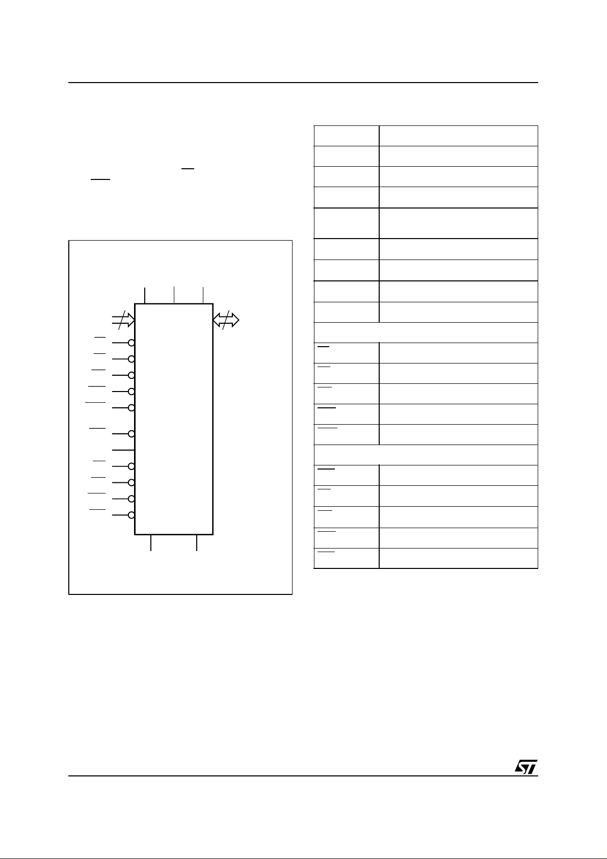
Figure 1. Packages
FBGA
Stacked LFBGA66 (ZA)
8 x 8 ball array
1/46November 2001
M36D232A, M36DR232B
DESCRIPTION
The M36DR232 is a multichip memory device containing a 32 Mbit boot block Flash memory and a
4MbitofSRAM.ThedeviceisofferedinaStacked
LFBGA66 (0.8 mm pitch) package.
Thetwo components are distinguished by use with
three chip enable inputs: EF
and, E1S
and E2S for t he SRAM. The two components are also separately power supplied and
grounded.
Figure 2. Logic Diagram
forthe Flash memory
Table 1. Signal Names
A0-A16 Address Inputs
A17-A20 Address Inputs for Flash Chip only
DQ0-DQ15 Data Input/Output
V
V
V
DDF
PPF
SSF
Flash Power Supply
Flash Optional Supply Voltage for Fast
Program & Erase
Flash Ground
A0-A20
EF
GF
WF
RPF
WPF
E1S
E2S
GS
WS
UBS
LBS
21
V
DDF
M36DR232A
M36DR232B
V
SSF
V
PPF
V
V
DDS
SSS
16
DQ0-DQ15
AI05440
V
DDS
V
SSS
NC Not Connected Internally
Flash control functions
EF
GF
WF
RPF
WPF
SRAM control functions
, E2S Chip Enable input
E1S
GS
WS
UBS
LBS
SRAM Power Supply
SRAM Ground
Chip Enable input
Output Enable input
Write Enable input
Reset input
Write Protect input
Output Enable input
Write Enable input
Upper Byte Enable input
Lower Byte Enable input
2/46
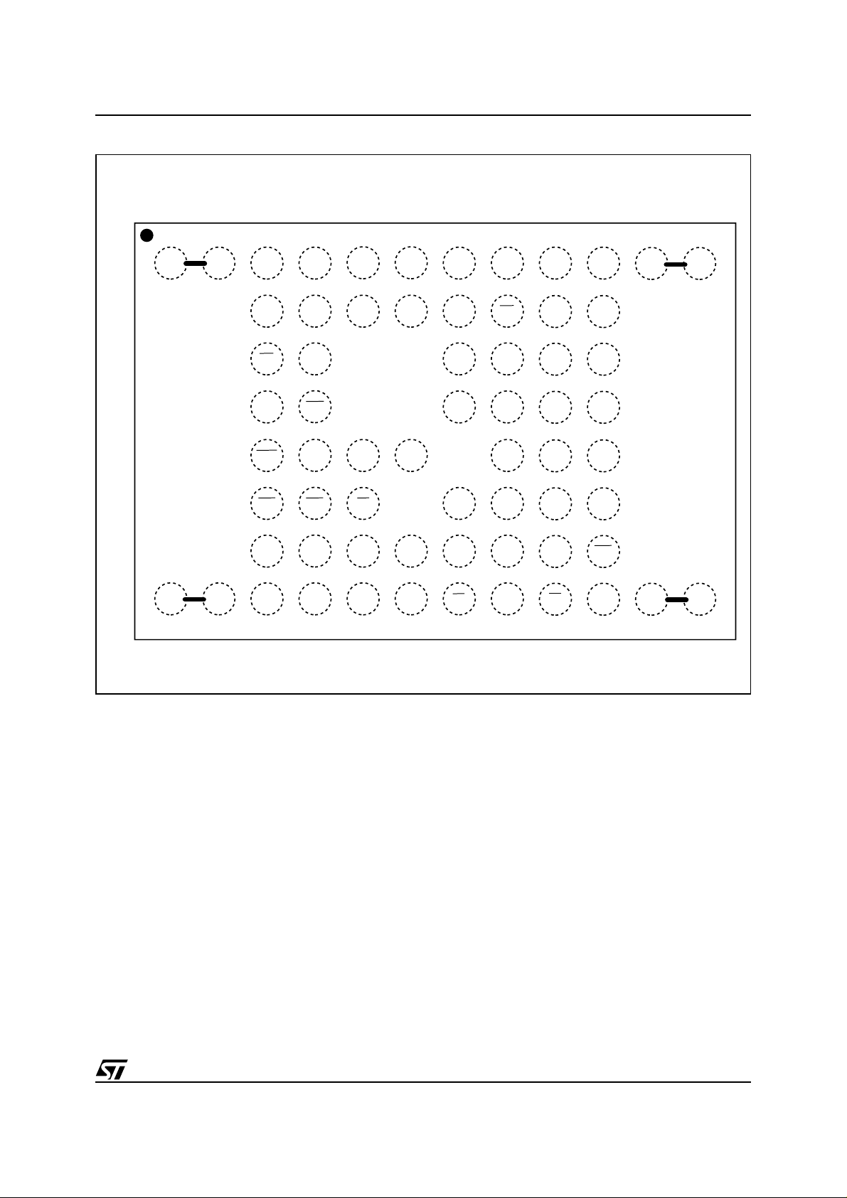
Figure 3. LFBGA Connections (Top view through package)
M36D232A, M36DR232B
#2#1
A
B
C
D
E
F
G
H
SSS
NC V
A8 A10
RPF
V
PPF
UBS
A17
A5
A15 A14
DQ11A19WPF
A13A11A20NCNC
DQ15A9A16
DQ9GSLBS
EFA0A4NCNC
A12
WS
DQ6DQ13NCWF
E2SDQ12V
DQ10
DQ8
A2A3A6A7A18
SSF
V
SSF
DQ14
DQ4
V
DDS
DQ7
DQ5
V
DQ3DQ2
DQ1DQ0
E1SA1
87654321
NC
DDF
NCNCGF
#4#3
NCNC
NC
AI90204
3/46
M36D232A, M36DR232B
Table 2. Absolute Maximum Ratings
(1)
Symbol Parameter Value Unit
T
A
T
BIAS
T
STG
(2)
V
IO
V
DDF
V
DDS
V
PPF
Note: 1. Except for the rating "Operating Temperature Range", stresses above those listed in the Table "Absolute Maximum Ratings" may
cause permanent damage to the device. These are stress ratings only and operation of the device at these or any other conditions
above those indicated in the Operating sections of t his specification is not implied. Exposure to Absolute Ma ximu m Rating conditionsf or extendedperiods mayaffect devicereliability. Referalso tothe STMicroelectronics SUREProgram andother relevantquality documents.
2. Minimum voltage may undershoot to –2V during transition and for less than 20ns.
3. Depends on range.
4. V
DD=VDDS=VDDF
Ambient Operating Temperature
Temperature Under Bias –40 to 125 °C
Storage Temperature –55 to 150 °C
Input or Output Voltage
Flash Chip Supply Voltage –0.5 to 2.7 V
SRAM Chip Supply Voltage –0.2 to 2.6 V
Program Voltage –0.5 to 13.0 V
.
(3)
–40 to 85 °C
–0.2 to V
DD
(4)
+0.3
V
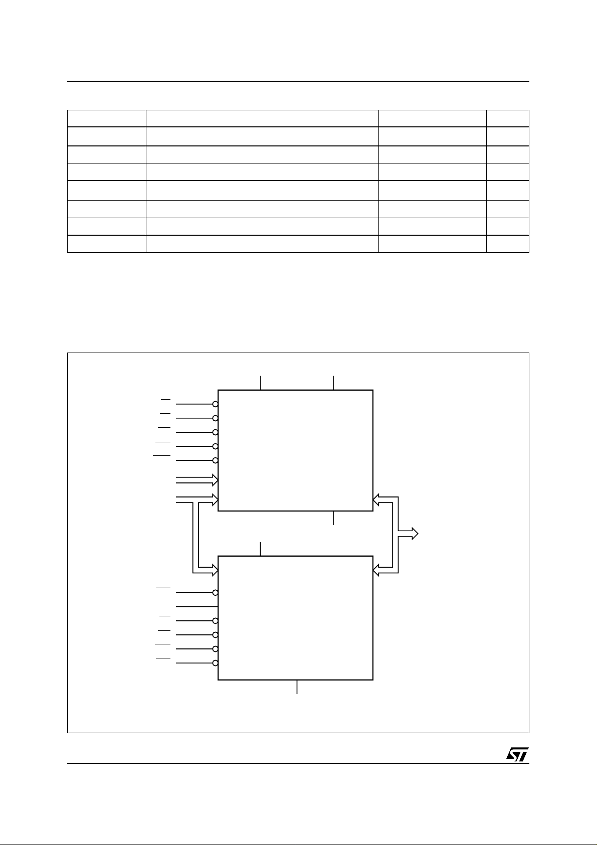
Figure 4. Functional Block Diagram
V
DDF
V
PPF
EF
GF
WF
RPF
WPF
A17-A20
A0-A16
E1S
E2S
GS
WS
UBS
LBS
Flash Memory
32 Mbit (x16)
V
DDS
2 Mbit (x16)
SRAM
V
SSF
DQ0-DQ15
4/46
V
SSS
AI05441

SIGNAL DESCRIPTIONS
See Figure 2 and Table 1.
Address Inputs (A0-A16). Addresses A0 to A16
are common inputs for the Flas h chip and the
SRAM chip. The address inputs for the Flash
memory are latched during a write operation on
the falling edge of the Flash Chip Enable (EF
Write Enable ( WF
), while address inputs fo r the
)or
SRAM array are latched during a w rite operation
on the falling edge of the SRAM Chip Enable lines
or E2S ) or Write Enable (WS).
(E1S
Address Inputs (A17-A20). Addres s A17 to A 20
are address inputs for the Flash chip. They are
latched during a write operation on the falling edge
of Fl as h Ch ip Ena ble (EF
) or Write Enable (WF).
Data Input/Outputs (DQ0-DQ15). The input is
data to b e programmed in the Flash or SRAM
memory array or a comm and to be written to the
C.I. of the Flash chip. Both are latched on the rising edge of Flash Chip Enable (EF
able (W F
E2S) or Write Enable (WS
) and, SRAM Chip Enable lines (E1S or
). The output is data
)orWriteEn-
from the Flash memory or SRAM array, the Electronic Signature Manufacturer or Device codes or
the Status register Data Polling bit DQ7, the Toggle Bits D Q6 and DQ2, the Error bit DQ5 or the
Erase Timer bit DQ3. Outputs are valid when
Flash Chip Enable (EF
SRAM Chip Enable lines (E1S
Enable (GS
) are active. The output is high imped-
) and Output Enable (GF)or
or E2S) and Output
ance when the both the Flash chip and the SRAM
chip are deselected or the outputs are disabled
and when Reset (RPF
Flash Chip Enabl e (EF
)isataVIL.
). The Chip Enable input
for Flash activates the memory control logic, input
buffers, decoders and sense amplifiers. EF
at V
IH
deselects the memory and reduces the power consumption to the standby level and output do Hi-Z.
canalsobeusedtocontrolwritingtothecom-
EF
mand register and to the Flash memory array,
while WF
remains at VIL.ItisnotallowedtosetEF
at VIL,E1Sat VILand E2S at VIHat the same time.
Flash Write Enable (WF
). The Write Enable in-
put controls writing to the Command Register of
theFlashchipandAddress/Datalatches.Dataare
latched on the rising edge of WF
Flash Output Enable (GF
.
). The Output Enable
gates the outputs through the data buffers during
a read operation of the Flash chip. When GF
WF
are High the outpu ts are High impedance.
Flash Reset/Power Down Input (RPF
). The RPF
and
input provides hardware reset of the memory
(without affecting the Configuration Register status), and/or Power Down fun ctions, depending on
the Configuration Regis ter status. Reset/Power
Down of the memory is achieved by pulling RPF
V
for at least t
IL
. When the reset pulse is giv-
PLPH
to
M36D232A, M36DR232B
en, if the memory is in Read, Erase Suspend Read
or Standby, it will output new valid dat a in t
after the rising edge of RPF.Ifthememoryisin
Erase or Program modes, the operation wi ll be
aborted and the res et recovery will take a maximum of t
Power Down (when enabled) in t
rising edge of RPF
. The mem ory will recover from
PLQ7V
PHQ7V2
. See Tables 1, 26 and Figure
11.
Flash Write Protect (WPF
). Write Protect is an
input to prot ect or unprotect the two lockable parameter blocks of the Flash memory. When WPF
is at VIL, the lock able blocks are protected. P r ogram or erase operations are not achievable.
When WPF
is at VIH, the lockable blocks are unprotected and they can be programmed or erased
(refer to Table 17).
SRAM Chip Enable (E1S
,E2S). The Chip En-
able input s for SRAM activate the mem ory control
logic, input buffers and decoders. E1S
E2S at V
deselects the me mory and reduces the
IL
power consumption to the standby level. E1S
E2S can also be used to control writing to the
SRAM memory array, while WS
is not al lowed to s et EF
at th e same time.
at V
IH
SRAMWriteEnable(WS
at VIL,E1Sat VILand E2S
). The Write Enable in-
remains at VIL.It
put cont ro ls writing to the SR A M m emory array.
WS
is active low.
SRAM Output Enable (GS
). T he Output Enable
gates the outputs through the data buffers during
a read operation of the SRAM chip. GS
low.
SRAM Upper Byte Enable (UBS
). Enable the
upper bytes for SRAM (DQ8-DQ 15). UBS
low.
SRAM Lower Byte Enable (LBS
). Enable the
lower bytes for SRAM (DQ0-DQ 7). LBS
low.
Supply Voltage(1.65 Vto 2.2V). Flash memo-
V
DDF
ry power supply for all operations (Read, Program and
Erase).
Programming Voltage (11.4V to 12.6V).
V
PPF
Used to provide high v oltage for f as t factory programming. High voltage on V
pin is required to
PPF
use the Double Word Program instruction. It is
also possible to perform word prog ram or erase instructions with V
Supply Voltage (1.65V to 2.2V). SRAM
V
DDS
pin grounded.
PPF
power supply for all operation s (Read, Prog ram).
V
SSF
and V
Ground. V
SSS
SSF
and V
reference for all v olt age measurements respectively in the Flash and SRAM chips.
PHQ7V1
after the
at VIHor
is active
isactive
is active
are the
SSS
and
5/46
M36D232A, M36DR232B
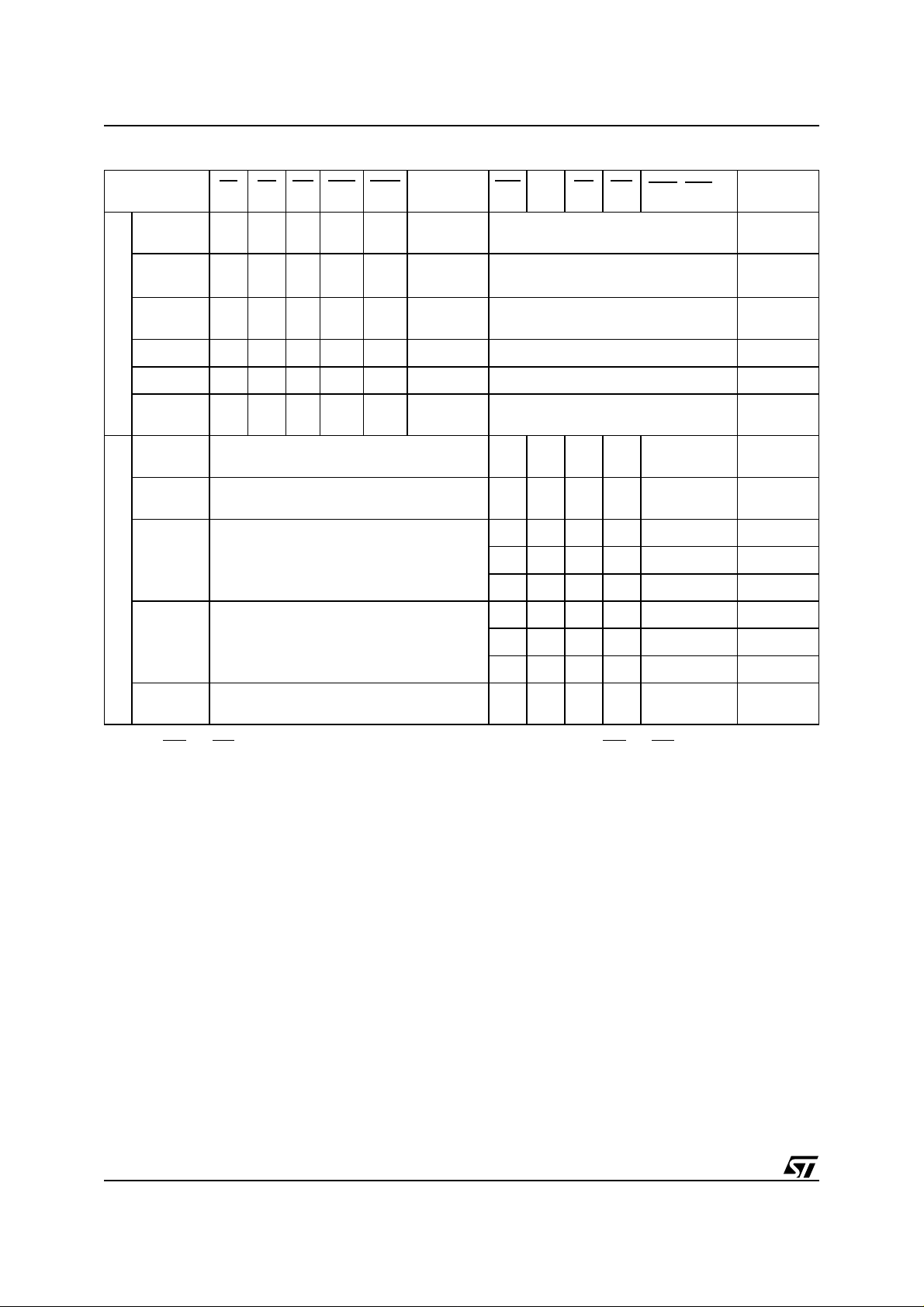
Table 3. Main Operation Modes
Operation
Mode
Read
Write
Block
Locking
Standby
Flash Memory
Reset X X X
Output
Disable
Read Flash must be disabled
Write Flash must be disabled
Standby/
Power
Down
SRAM
Data
Retention
Output
Disable
Note: X = VILor VIH,V
1. If UBS
and LBS are tied together the bus is at 16 bit. For an 8 bit bus configuration use UBS andLBS separately.
GF WF RPF WPF
EF
V
ILVILVIHVIH
V
ILVIHVILVIH
V
IL
V
IH
XX
XX
V
V
V
V
ILVIHVIHVIH
Any Flash mode is allowable
Any Flash mode is allowable
Any Flash mode is allowable
=12V±5%.
PPFH
V
PPF
E1S E2S GS WS
UBS,LBS
X Don't care SRAM must be disabled
V
or
V
IH
V
IH
IL
X Don't care Any SRAM mode is allowable Hi-Z
IH
X Don't care Any SRAM mode is allowable Hi-Z
IL
CCF
V
PPFH
SRAM must be disabled Data Input
Don't care SRAM must be disabled X
X Don't care Any SRAM mode is allowable Hi-Z
V
ILVIHVILVIH
V
ILVIHVIHVIL
V
XXX X Hi-Z
IH
V
X
X X X Hi-Z
IL
XXXX
V
XXX X Hi-Z
IH
V
X
X X X Hi-Z
IL
XXXX
V
ILVIHVIHVIH
V
IL
V
IL
V
IH
V
IH
X Hi-Z
(1)
DQ15-DQ0
Data
Output
Data out
Word Read
Data in
Word Write
Hi-Z
Hi-Z
6/46

FLASH M EMO RY COMPONENT
Organization
The Flash Chip is organized as 2Mb x16 bits. A0A20 are the address lines, DQ0-DQ15 are the
Data Input/Output. Memory control is provided by
Chip Enable EF
able W F
Reset RPF
, Output Enable GF and Write En-
inputs.
is used to reset all the mem ory circuitry
and to set the chip in power down mode if this
function is enabled by a p roper setting of the Configuration Register. Erase and Program operations
are controlled by an internal Program/Erase Controller (P/E.C.). Status Register data output on
DQ7 provides a DataPolling signal, DQ6 and DQ2
provide Toggle signals and DQ5 provides error bit
to indicate the state of the P/E.C operat ions.
Memory Blocks
The device features asymmetrically b locked architecture. The Flash Chip has an array of 71 blocks
and is divided into two bank s A and B, providing
Dual Bank operations. While programming or
erasing in Bank A, read operations are possible
into Bank B or vice versa. The memory also features an erase s us pend allowing to read or program in another block wi thin the sam e bank. Once
suspended t he erase can be resumed. The Bank
Size and Sectorization are summarized in Table 4.
Parameter Blocks are located at the top of the
memory address space for the T op version, and at
the bottom for the Bottom version. The memory
maps are shown in Tables 5, 6, 7 and 8.
The Program and Erase operations are m anaged
automatically by the P/E.C. Block protection
against Program or Erase provides additional data
security. All blocks are protected at Power Up. Instructions are provided to protect or unprotect any
block in the application. A second register locks
the protection status while WPF
is low (see Block
Locking description). The Reset command does
not af fect the configuration of unprotected blo cks
and the Configuration Re giste r status.
Device Operations
The following operations can be performed using
the appropriate bus cycles: Read Array (Random,
and Page Modes), Write command, Output Disable, Standby, Res et/Power Down and Block
Locking. See Table 9.
Read. Read operations are used to output the
contents of the Memory Array, the Electronic Signature, t he Status Reg ister, the CFI, the Block
Protection Status or the Configurat ion Register
status. Read operation of the memory array is performed in asynchronous page mode, that provides
fast access time. Data is internally read and stored
in a page buf fer. The page has a size of 4 words
M36D232A, M36DR232B
and is ad dres se d by A0-A1 address inputs. Read
operations of the Electronic Signature, the Status
Register, the CFI, the Block Protection Status, the
Configuration Register status and the Security
Code are performed as single asynchronous read
cycles (Random Read). Both Chip Enable EF
Output Enable GF
must be at VILin order to read
the out put of the memory.
Write. Write operations are used to give Instruc-
tion Co mm ands to the memory or to latch I nput
Data to be programmed. A write operation is initiated when Chip Enable EF
and Write Enable WF
are a t VILwith Output Enable GF at VIH.Addresses are latched on the falling edge of W F
whichever occurs last. Commands and Input Data
are latched on th e rising edge of WF
or EF whichever occurs first. Noise pulses of less than 5ns typical on EF
,WFand GF signals do not st art a write
cycle.
Dual Bank Operations. The Dual Bank allows to
read data from one bank of memory while a program or erase operation is in progress in the other
bank of the memory. Read and Write cycles can
be initiated for simultaneous operat ions in different
banks w ithout any d elay. Status Register during
Program or Erase m ust be monit ored using an address w ithin t he bank b eing modified.
Output Disable. The data outpu ts are high impedance when t he Output Enable GF
Write Enable WF
at VIH.
is at VIHwith
Standby. The m emory is in standby when Chip
Enable EF
is at VIHand the P/E.C. is idle. The
power consumption is reduced to the standby level
and the out puts are high impedance, inde pendent
of t he Output Enable GF
or Write Enable WF in-
puts.
Automatic Standby. When in Read mode, after
150ns of bus inactivity and when CMO S levels are
driving the addresses, the chip automat ically enters a pseudo-s tan dby mode where c ons umption
is red uc ed to the CMOS standby value, while outputs still drive the bus.
Power Down. Th e memory is in Power Down
when the Configuration Register is s et for Power
Down and RPF
is a t VIL. The power consumption
is reduced to the Power Down level, and Outp uts
are in high impedance , independent of the Chip
Enable EF
, Output Enable GF or Write Enable WF
inputs.
Block Locking. Any combination of blocks can
be temporarily protected again st Program or
Erase by setting the lock register and pulling WPF
to VIL(see Block Lock instruction).
and
or EF
7/46
M36D232A, M36DR232B
Table4.BankSizeandSectorization
Bank Size Parameter Blocks Main Blocks
Bank A 4 Mbit 8 blocks of 4 KWord 7 blocks of 32 KWord
Bank B 28 Mbit - 56 blocks of 32 KWord
Table 5. Bank A, Top Boot Block Addresses
M36DR232A
#
0 4 1FF000h-1FFFFFh
1 4 1FE000h-1FEFFFh
2 4 1FD000h-1FDFFFh
3 4 1FC000h-1FCFFFh
4 4 1FB000h-1FBFFFh
5 4 1FA000h-1FAFFFh
6 4 1F9000h-1F9FFFh
7 4 1F8000h-1F8FFFh
8 32 1F0000h-1F7FFFh
9 32 1E8000h-1EFFFFh
10 32 1E0000h-1E7FFFh
11 32 1D8000h-1DFFFFh
12 32 1D0000h-1D7FFFh
13 32 1C8000h-1CFFFFh
14 32 1C0000h-1C7FFFh
Size
(KWord)
Address Range
Table 6. Bank B, Top Boot Block Addresses
M36DR232A
#
0 32 1B8000h-1BFFFFh
1 32 1B0000h-1B7FFFh
2 32 1A8000h-1AFFFFh
3 32 1A0000h-1A7FFFh
4 32 198000h-19FFFFh
5 32 190000h-197FFFh
6 32 188000h-18FFFFh
7 32 180000h-187FFFh
8 32 178000h-17FFFFh
9 32 170000h-177FFFh
10 32 168000h-16FFFFh
11 32 160000h-167FFFh
12 32 158000h-15FFFFh
13 32 150000h-157FFFh
14 32 148000h-14FFFFh
15 32 140000h-147FFFh
16 32 138000h-13FFFFh
Size
(KWord)
Address Range
17 32 130000h-137FFFh
18 32 128000h-12FFFFh
19 32 120000h-127FFFh
20 32 118000h-11FFFFh
21 32 110000h-117FFFh
22 32 108000h-10FFFFh
23 32 100000h-107FFFh
24 32 0F8000h-0FFFFFh
25 32 0F0000h-0F7FFFh
26 32 0E8000h-0EFFFFh
27 32 0E0000h-0E7FFFh
28 32 0D8000h-0DFFFFh
29 32 0D0000h-0D7FFFh
30 32 0C8000h-0CFFFFh
31 32 0C0000h-0C7FFFh
32 32 0B8000h-0BFFFFh
33 32 0B0000h-0B7FFFh
34 32 0A8000h-0AFFFFh
35 32 0A0000h-0A7FFFh
36 32 098000h-09FFFFh
37 32 090000h-097FFFh
38 32 088000h-08FFFFh
39 32 080000h-087FFFh
40 32 078000h-07FFFFh
41 32 070000h-077FFFh
42 32 068000h-06FFFFh
43 32 060000h-067FFFh
44 32 058000h-05FFFFh
45 32 050000h-057FFFh
46 32 048000h-04FFFFh
47 32 040000h-047FFFh
48 32 038000h-03FFFFh
49 32 030000h-037FFFh
50 32 028000h-02FFFFh
51 32 020000h-027FFFh
52 32 018000h-01FFFFh
53 32 010000h-017FFFh
54 32 008000h-00FFFFh
55 32 000000h-007FFFh
8/46
M36D232A, M36DR232B
Table7.BankB, Bottom BootBlockAddresses
M36DR232B
#
55 32 1F8000h-1FFFFFh
54 32 1F0000h-1F7FFFh
53 32 1E8000h-1EFFFFh
52 32 1E0000h-1E7FFFh
51 32 1D8000h-1DFFFFh
50 32 1D0000h-1D7FFFh
49 32 1C8000h-1CFFFFh
48 32 1C0000h-1C7FFFh
47 32 1B8000h-1BFFFFh
46 32 1B0000h-1B7FFFh
45 32 1A8000h-1AFFFFh
44 32 1A0000h-1A7FFFh
43 32 198000h-19FFFFh
42 32 190000h-197FFFh
41 32 188000h-18FFFFh
40 32 180000h-187FFFh
39 32 178000h-17FFFFh
38 32 170000h-177FFFh
37 32 168000h-16FFFFh
36 32 160000h-167FFFh
35 32 158000h-15FFFFh
34 32 150000h-157FFFh
33 32 148000h-14FFFFh
32 32 140000h-147FFFh
31 32 138000h-13FFFFh
30 32 130000h-137FFFh
29 32 128000h-12FFFFh
28 32 120000h-127FFFh
27 32 118000h-11FFFFh
26 32 110000h-117FFFh
25 32 108000h-10FFFFh
24 32 100000h-107FFFh
23 32 0F8000h-0FFFFFh
22 32 0F0000h-0F7FFFh
21 32 0E8000h-0EFFFFh
20 32 0E0000h-0E7FFFh
19 32 0D8000h-0DFFFFh
Size
(KWord)
Address Range
18 32 0D0000h-0D7FFFh
17 32 0C8000h-0CFFFFh
16 32 0C0000h-0C7FFFh
15 32 0B8000h-0BFFFFh
14 32 0B0000h-0B7FFFh
13 32 0A8000h-0AFFFFh
12 32 0A0000h-0A7FFFh
11 32 098000h-09FFFFh
10 32 090000h-097FFFh
9 32 088000h-08FFFFh
8 32 080000h-087FFFh
7 32 078000h-07FFFFh
6 32 070000h-077FFFh
5 32 068000h-06FFFFh
4 32 060000h-067FFFh
3 32 058000h-05FFFFh
2 32 050000h-057FFFh
1 32 048000h-04FFFFh
0 32 040000h-047FFFh
Table8.BankA, Bottom BootBlockAddresses
M36DR232B
#
14 32 038000h-03FFFFh
13 32 030000h-037FFFh
12 32 028000h-02FFFFh
11 32 020000h-027FFFh
10 32 018000h-01FFFFh
9 32 010000h-017FFFh
8 32 008000h-00FFFFh
7 4 007000h-007FFFh
6 4 006000h-006FFFh
5 4 005000h-005FFFh
4 4 004000h-004FFFh
3 4 003000h-003FFFh
2 4 002000h-002FFFh
1 4 001000h-001FFFh
0 4 000000h-000FFFh
Size
(KWord)
Address Range
9/46
M36D232A, M36DR232B
Table 9. User Bus Operations
(1)
Operation EF GF WF RPF WPF DQ0-DQ15
Write
Output Disable
Standby
V
IL
V
IL
V
IH
Reset / Power Down X X X
Block Locking
Note: 1. X = Don't care.
V
IL
V
IH
V
IH
V
IL
V
IH
XX
XX
V
IH
V
IH
V
IH
V
IL
V
IH
Table 10. Read Electronic Signature (AS and Read CFI instructions)
Code Device EF
Manufacturer Code
M36DR232A
Device Code
M36DR232B
GF WF A0 A1 A2-A7
V
V
V
IL
IL
V
V
IL
IL
V
V
IL
IL
IH
V
IHVIH
V
IHVIH
V
IL
V
V
V
0 Don't Care 20h 00h
IL
0 Don't Care A0h 00h
IL
0 Don't Care A1h 00h
IL
Table 11. Read Bl ock Protecti on (AS and Read CFI instructions)
Block Status EF
GF WF A0 A1 A2-A7
Other
Addresses
A12-A20 DQ0 DQ1 DQ2-DQ15
Other
Addresses
V
IH
V
IH
V
IH
V
IH
V
IL
Data Input
Hi-Z
Hi-Z
Hi-Z
X
DQ0-DQ7 DQ8-DQ15
Protected Block
Unprotected Block
Locked Block
V
ILVILVIHVILVIH
VILVILVIHVILV
V
ILVILVIHVILVIH
0 Don't Care Block Address 1 0 0000h
0 Don't Care Block Address 0 0 0000h
IH
0 Don't Care Block Address X 1 0000h
Table 12. Read Con f iguration Regi ster (AS and Read CFI instructions)
Function EF GF WF A0 A1 A2-A7 Other Addresses DQ10
RPF
V
V
V
V
Reset
Reset/Power Down
IL
IL
IH
V
V
IL
V
IL
IH
V
IH
V
V
IH
0 Don't Care 0 Don't Care
IH
0 Don't Care 1 Don't Care
IH
DQ0-DQ9
DQ11-DQ15
10/46
INSTRUCTIONS AND COMMANDS
Seventeen instructions are def ined (s ee Table
15), and the internal P / E.C. automat icall y ha ndles
all timi ng and verification of the Program and
Erase operat ions. The Status Register Data Polling, Toggle, Error bits can be read at any time, during programming or erase, to monitor the progress
of t he operation.
Instructions, made up of one or more commands
writtenincycles,canbegiventotheProgram/
Erase Controller through a Command Interface
(C.I.). The C.I. latches commands written to the
memory. Commands are made o f address and
data sequences . Two Coded Cycles unlock the
Command Interface. They are followed by an input
command or a confirmation command. The Coded
Sequence consists of writing the data AAh at the
address 555h during the first cycle and the data
55h at the address 2AAh during the s ec ond cycle.
Instructions are composed of up to six cycles. The
first two cycles input a Coded Sequence to the
Command Interface which is common to all instructions (see Table 15). The third cycle inputs
the instruction set-up command. Subsequent cycles output the addressed data, Electronic Si gnature, Block Protection, C onfiguration Register
Status or CF I Query for Read operat ions. In order
to give additional data protection, the instructions
for Block Erase and Bank Eras e require further
command inputs. For a Program instruction, the
fourthcommandcycleinputs the ad dress and data
to be programmed. For a Double Word Programming instruction, the fourth and fifth command cycles input the address and data to be
programmed. For a Block Erase and Bank Erase
instructions, the fourth and fifth cycles input a further Coded Sequence before the Erase co nfirm
command on the sixth cycle. Any combination of
blocks of the same memory bank can be erased.
Erasure of a memory block may be suspended, in
order to read data from another block or to program data in another block, and then resumed.
When powerisfirst applied the command interface
is reset to Read Array.
Command sequencing must be followed exactly.
Any invalid combination of commands will reset
the device to Read Array. The inc re as ed number
of cycles has been chosen to ensure maximum
data security.
M36D232A, M36DR232B
Table 13. Commands
Hex Code Command
00h Bypass Reset
10h Bank Erase Confirm
20h Unlock Bypass
30h Block Erase Resume/Confirm
40h Double Word Program
Block Protect, or
60h
80h Set-up Erase
90h
98h CFI Query
A0h Program
B0h Erase Suspend
F0h Read Array/Reset
Read/Reset (RD) I nstruction. The Read/Reset
instruction cons ists of one write cycle givin g the
command F0h. It can be optionally p receded by
the two Coded Cycles. Subsequent read operations will read the me mory array addressed and
output the data read.
CFI Query (RCFI) Instruction. Common Flash
Interface Query m ode is entered writing 98h at address 55h. The CFI data structure gives information on the device, such as the sectorization, the
command set and some electrical specifica tions.
Table 18, 19, 20 and 21 show the addresses used
to retr ieve each data. The CFI data structure contains also a security area; in this sect ion, a 64 bit
unique security number is written, starting at address 80h. This area can be accessed only in read
mode by the final user and there are no ways of
changing the code af te r it has been written by ST.
Write a read instruction (RD) to return to Read
mode.
Auto Select (AS) Instruction. This instruction uses
two Coded Cycles followed by one write cycle giving the command 90h to address 555h for command set-up. A subsequent read will outpu t the
Manufacturer or th e Device Code (Electronic Signature), the Block Protection status or the Configuration Register status depending on the levels of
A0 and A1 (see Table 10, 11 and 12). A7-A2 must
be at V
Block Unprotect, or
Block Lock, or
Write Configuration Register
Read Electronic Signature, or
Block Protection Status, or
Configuration Register Status
, while other address input are ignored.
IL
11/46

M36D232A, M36DR232B
The bank address is don’t care f or this instruction.
The Electronic Signature can be read from the
memory allowing program min g equipment or applications to automatic ally match their interfac e to
the characteristics of Flash Chip. The Manufac turer Code is output when the address lines A0 and
A1 are at V
is at V
, the Device Code is output when A0
IL
with A1 at VIL.
IH
The codes are output on DQ 0-DQ7 with DQ8DQ15 at 00h. The AS instruction also allows the
access to the Block Protection Status. After giving
the AS instru ction, A0 is s et to V
with A1 at VIH,
IL
while A12-A20 define the address of the block to
be verified. A read in these conditions will output a
01h if the block is p ro tected and a 00h if the block
is not protected.
The AS Instruction final ly allows the access to the
Configuration Register status if both A0 and A1
are s et to V
is active as RPF
. If DQ10 is '0' only the Reset function
IH
is set to VIL(default at power-up).
If DQ10 is '1' both the Reset and the Power Down
functions will be achieved by pulling RPF
to VIL.
The other bits of the Con figurati on Register are reserved and must be ignored. A reset command
puts t he dev ice in read array mode.
Write Configuration Register (CR) Instruction. Th is instruction uses two Code d Cycles fol-
lowed by one write cycle giving the command 60h
to address 555h. A further write cycle giving the
command 03h writes the contents of address bits
A0-A15 to the 16 bits configurat ion register. Bits
written by inputs A0-A9 and A11-A15 are reserved
for future use. Address input A10 defines the status of the Reset/Power Down functions. It mus t be
set to V
V
IH
to enable only the Reset function and to
IL
to enable also the Power Down function. At
Power Up all the Configuration Register bits are
reset to '0'.
Enter Bypass Mode (EBY) Instruction. This instruction uses the two Coded cycles followed by
one write cycle giving the command 20h to address 555h for mode set-up. Onc e in By pas s
mode, the device will accept the Exit Bypass
(XBY) and Program or Double Word Program in
Bypass mode (P GBY, DPGBY) comm ands. The
Bypass mode allows to reduce th e overall programming time when l arge memory arrays need to
be programmed.
Exit Bypass Mode (XBY) Instruction. This in-
struction uses t wo write cycles. The first inputs to
the memory the command 90h and the second inputs the Exit Bypass mode confirm (00h). After the
XBYinstruction, the device resetsto Read Memory Arra y mode.
Program in Bypass Mode (PGBY) Instruction. This instruction uses two write cycles. The
Program command A0h is written to any Address
on the first cycle and the second write cycle latch-
esthe A ddresson the falling edge of WF
or EF and
the Data to be written on t he rising edge and starts
the P/E.C. Read operations within the same bank
output the Status R egister bits af ter the program ming has started. Memory programming is m ade
only by writing '0' in place of '1'. Status bit s DQ6
and DQ7 determine if programming is on-going
and DQ5 allows verification of any possible error.
Program (PG) Instruction. This instruction uses
four write cycles. The Program command A0h is
written to address 555h on the t hird cycle after two
Coded Cycles. A fourth w rite operation latches the
Address and the Data to be written and starts t he
P/E.C. Read operations within the sam e bank output the Status Register bits after the programming
has sta rted. Memory programming is made only
by writing '0' in place of '1'. Status bits DQ6 and
DQ7 determine if programming is on-going and
DQ5 allows verification of any possible error. Programming at an address not in blocks being
erased is also possible during erase su spend.
Double Word Program (DPG) Instruction. This
feature is offered to improve the programming
throughput, writing a page of two adjacent words
in parall el. High voltage (11.4V to 12. 6V ) on V
PP
pin is required. This instruction uses five write cycles. The double word program command 40h is
written to address 555h on the t hird cycle after two
Coded Cycles. A fourth write c ycle latches the address and data t o be written to the first location. A
fifth write cycle latches the new data to be written
to the s ec ond location and starts the P/E.C.. Note
thatt he two locations must h av e the sam e address
except for the address bit A0. The Double Word
Program can be executed in Bypass mode (DP GBY) to skip the two coded cycles at the beginning
of each command.
Block Protect (BP), Block U nprotect (BU),
Block Lock (BL) Instructions. All blocks are
protected at power-up. Each block of the array has
two levels of prot ec tion against program or erase
operation. The first level is set by the Block Protect
instruction; a p rotect ed block cannot be programmed or erased until a Block Unprotect instruction is given for that block. A second level of
protection is set by the Block Lock instruction, and
requires the use of the WPF
pin, according to the
following scheme:
– when WPF
is at VIH, the Lock status is overridden and all blocks can be protected or unprotected;
– when WP F
is at VIL, Lock status is enabled; the
locked blocks are protected, regardless of their
previous protect state, and protection status
cannot be chan ged. Blocks that are not lock ed
can still change their protection status, and program or erase ac c ordingl y;
12/46

M36D232A, M36DR232B
– the loc k status is cleared for all blocks at power
up; once a block has been locked s tate can be
cleared only with a reset command. T he protection and lock status can be m onit ored for each
block using the Autoselect (A S) instruction. Protected blocks wil l output a ‘1’ on DQ0 and lock ed
blocks will out put a ‘1’ on DQ1.
Refer to Table 14 for a list of the protection state s.
Block Erase (BE) In struction. This instruction
uses a m inimum of six write cycles. The Erase
Set-up command 80h is written to address 555h
on third cycle after the two Coded cycles. The
Block Erase Confirm c ommand 30h is similarly
written on the sixth cycle after another two Coded
cycles and an address within the block to be
erased is given an d latched in to the memory.
Additional block Erase Confirm commands and
block addresses can be written subsequently to
erase other blocks in parallel, without further Coded cycles. All blocks must belong to the same
bank of memory; if a new block belongi ng to the
other bank is given, the operation is abort ed. The
erase will start a fter an erase timeout period of
100µs. Thus, additional Erase Confirm commands
for other blocks must be given within this delay.
The input of a new Erase Confirm c ommand will
restart the time out period. The status of the internal timer can be monitored through the level of
DQ3, if DQ3 is '0' the Block Erase Comm and has
been given and the timeout is running, if DQ3 is '1',
the timeout has expired an d the P/E.C. is erasing
the Block(s). If the second command given is not
an erase confirm or if the Coded cycles are wrong,
the instruction aborts, and the dev ice is reset to
Read Array. It is not necessary to program t he
block with 00h as the P/E.C. will do this automatically before erasing to FFh. Read operations within the same bank, after the sixth rising edge of WF
or EF, output the s tatus register bits.
During the execution of the erase by the P/E.C.,
the memory accepts only the Erase Susp end ES
instruction; the Read/Reset RD instruction is accepted during the 100µs time-out perio d. Data
Polling bit DQ7 returns '0' while the erasure is in
progress and '1' when it has completed. The Toggle bit DQ6 toggles during the erase operation,
and stops when erase is completed.
After completion the Status Register bit DQ5 returns '1' if there has been an erase f ailure. In such
a situat ion, the Toggle bit DQ2 can be used to determine which block is not correctly erased. In the
case of erase failure, a Read/Reset RD instruction
is nece ssary in order to reset the P /E.C.
Bank Erase (BKE) Instruction. This instruction
uses s ix w rite cycles and is used to erase all the
blocks belonging to t he s elected bank. The Er as e
Set-up command 80h is written to address 555h
on the third cycle after the two Coded cycles. T he
Bank Erase Confirm command 10h is similarly
written on the sixth cycle after another two Coded
cycles at an address within the selected bank . If
the second command given is not an erase confirm or if the Coded cycles are wrong, the instruction aborts a nd the device is reset to Read Array.
It is not necessary to program the array with 00h
first as the P/E.C. will automatically do this before
erasing it to FFh. Read operations within the same
bank after the sixth rising edge of WF
or EF output
the Status Register bits. During the execution of
the erase by the P/E.C., Data Polling bit DQ7 returns '0', then '1' on completion. The Toggle bit
DQ6 toggles during erase operation and stops
when erase is completed. A fter completion the
Status Register bit DQ5 returns '1' if there has
been an Erase Failure.
Erase Suspend (ES) Instruction. In a dual bank
memory the Erase Suspend instruction is used to
read data within the bank where erase is in
progress. It i s also possibl e to program data in
blocks not being erased.
The Erase Suspend instruction consists of writ ing
the command B0h without any specific address.
No Coded Cycles are required. Erase suspend is
accepted only during the Block Erase instruction
execution. The Toggle bit DQ6 stops toggling
when the P/ E.C. is suspended within 15µs after
the Eras e Suspend (ES) command has b een written. The device will then automatically be set t o
Read Memory Array mode. When erase is suspended, a Read from blocks being erased will output DQ2 toggling and DQ 6 at '1'. A Read from a
block not being erased returns valid data. During
suspension the memory will respond only to the
Erase Resume ER and the Program PG instructions. A Program operation can be initiated during
erase suspend in one of the blocks not being
erased. It will result in DQ6 toggling when the dat a
is be ing program med.
Erase Resume (ER) Instruction. If an Erase
Suspend instruction was previously executed, the
erase operation may be resumed by giving the
command 30h, at an address within the bank being eras ed and without an y Coded Cycle.
13/46
M36D232A, M36DR232B
Table 14. Pro t ecti on States
(2)
Current State
(WP, DQ1, DQ0)
Program/Erase
Allowed
(1)
Next State After Event
(3)
Protect Unprotect Lock WP transition
100 yes 101 100 111 000
101 no 101 100 111 001
110 yes 111 110 111 011
111 no 111 110 111 011
000 yes 001 000 011 100
001 no 001 000 011 101
011 no 011 011 011
Note: 1. All blocksare protectedat power-up, so the defaultconfigurationis 001 or 101 accordingto WPF status.
2. Current state and Next state gives the protection status of a block. The protection status is defined by the write protect pin and by
DQ1(=1foralockedblock)andDQ0(=1foraprotectedblock)asreadintheAutoselectinstructionwithA1=V
3. Next state is the protection status of a block after a Protect or Unprotect or Lock command has been issued or after WPF
changed its logic value.
4. A WPF
Table 15. Instructions
transition to VIHon a locked block will restore the previous DQ0 value, giving a 111 or 110.
(1,2)
111 or 110
andA0=VIL.
IH
Mne. Instr. Cyc. 1st Cyc. 2nd Cyc. 3rd Cyc. 4th Cyc. 5th Cyc. 6th Cyc.
RD
Read/Reset
(4)
Memory Array
(3)
Addr.
1+
Data F0h
Addr. 555h 2AAh 555h
3+
Data AAh 55h F0h
X
Read Memory Array until a new write cycle is initiated.
Read Memory Array until a new
write cycle is initiated.
Addr. 55h
RCFI CFI Query 1+
Read CFI data until a new write cycle is initiated.
Data 98h
Addr. 555h 2AAh 555h Read electronic Signature or
AS
(4)
Auto Select 3+
Configuration
CR
Register Write
Data AAh 55h 90h
Addr. 555h 2AAh 555h
4
Block Protection or Configuration
Register Status until a new cycle
is initiated.
Configuration Data
Data AAh 55h 60h 03h
(4)
has
PG Program 4
DPG
EBY
Double Word
Program
Enter Bypass
Mode
14/46
Addr. 555h 2AAh 555h
Data AAh 55h A0h
Addr. 555h 2AAh 555h
5
Data AAh 55h 40h
Addr. 555h 2AAh 555h
3
Data AAh 55h 20h
Program
Address
Program
Data
Program
Address 1
Program
Data 1
Read Data Polling or
Toggle Bit until
Program completes.
Program
Address 2
Note 6, 7
Program
Data 2
 Loading...