

■ Compatible with SPI Bus Serial Interface
(Positive Clock SPI Modes)
■ Single Supply Voltage: 4.5 V to 5.5 V
■ 5 MHz Clock Rate (maximum)
■ Sixteen 16-bit Increment al Regist ers
■ BYTE and PAGE WRITE (u p to 32 Bytes)
(except for the Incremental Registers)
■ Self-Tim e d P ro g r amming Cycle
■ Hardware Protection of the Status Register
■ Resizeable Read-Only EEPROM Area
■ Enhanced ESD Protection
■ 1 Million Erase/Write Cycles (minimum)
■ 40 Year Data Retention (minimum)
DESCRIPTION
The M35080 device consists of 1024x8 bits of low
power EEPROM, fabricated with
STMicroelectronics’ proprietary High Endurance
Double Polysilicon CMOS technology.
The device is accessed by a simple SPI-compatible serial interface. The bus signals consist of a
serial clock input (C), a serial data input (D) and a
serial data output (Q), as shown in Table 1.
The device is selected when t he chip s elect input
) is held low. Data is clocked in during the low to
(S
high transition of the clock, C. Data is clocked out
during the high to low transition of the clock.
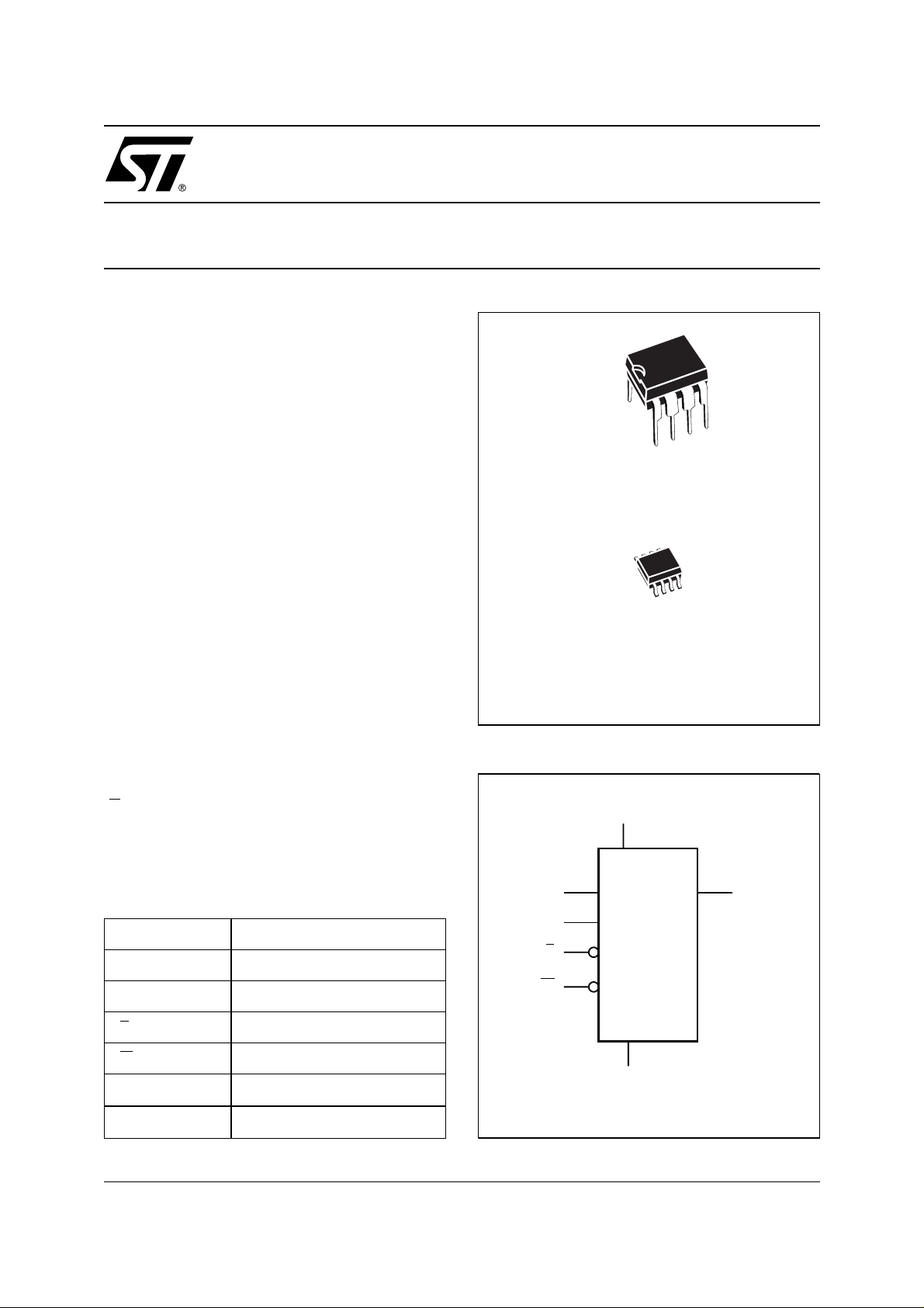
M35080
8 Kbit Serial SPI Bus EEPROM
With Incremental Registers
PRELIMINARY DATA
8
1
PSDIP8 (BN)
0.25 mm frame
8
1
SO8 (MN)
150 mil width
Figure 1. Logic Diagram
V
CC
D
Q
Table 1. Signal Names
W
C
S
M35080
V
SS
C Serial Clock
D Serial Data Input
Q Serial Data Output
S
W
V
CC
V
SS
June 1999
This is preliminary information on a new product now in development or undergoing evaluation. Details are subject to change without notice.
Chip Select
Write Protect
Supply Voltage
Ground
AI02143
1/18
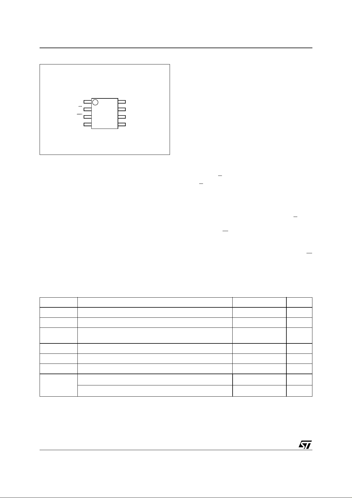
M35080
Figure 2. DIP and SO Connections
M35080
V
SS
Note: 1. NC = Not Connected.
W
1
S
2
3
4
Q
8
7
6
5
AI02144B
V
D
C
NC
CC
The memory is organized in pages of 32 bytes.
However, the first page is not treated in the sam e
way as the others. Instead, it is considered to consist of sixteen 16-bit incremental registers. Each
register can be modified using the conventional
write instructions, but the new value will only be
accepted if it is greater than the current value.
Thus, each register is restricted t o b eing mo dified
monotonically upwards.
This is useful in applications where it is necessary
to implement a counter that is protected from
fraudulent tampering (such as in a car odometer,
an electricity meter, or a tally for remaining credit).
SIGNAL DESCRIPTION
Seria l O utput ( Q )
The output pin is used to transfer data serially out
of the Memory. Data is shifted out on the falling
edge of the serial clock.
Serial Inpu t ( D )
The input pin is used to transfer data serially into
the device. Instructions, addresses, and the data
to be written, are each received t his way. Input is
latched on the rising edge of the serial clock.
Serial Clock (C)
The serial clock provides the timing for the serial
interface (as shown in Figure 3). Instructions, addresses, or data are latched, from the input pin, on
the rising edge of the clock input. The output dat a
on the Q pin changes state after the falling edge of
the clock input.
Chip Select (S
When S
is high, the memory device is deselected,
)
and the Q output pin is held in its high impe dance
state. Unless an internal write operation is underway, the memory device is placed in its stand-by
power mode.
After power-on, a high-to-low transition on S
is re-
quired prior to the start of any operation.
Write Protect (W
)
The protection features of t he m em ory device are
summarized in Table 3.
The hardware write protection, controlled by the W
pin, restricts write access to the Status Register
Table 2. Absolute Maximum Ratings
Symbol Parameter Value Unit
T
A
T
STG
T
LEAD
V
O
V
I
V
CC
V
ESD
Note: 1. Except for the rating “Operating Temperature Ra nge”, stres ses above those listed in the Table “Absolute Maximum Ratings” may
2/18
cause perm anent damage to the device. These are stress ratings only and op eration of th e device at these or any othe r
conditions above thos e i ndi cated in the O perating sec tions of this specificat i on i s not implied. Exposure to Absolute Ma xim um
Rating conditions for extended periods may affect device reliability. Refer also to the ST SURE Program and
other relevant quality documents .
2. MIL-STD-883C, 3015.7 (100 pF , 1500W).
3. EIAJ IC- 121 (Condi tion C) (200pF , 0W).
Ambient Operating Temperature -40 to 125 °C
Storage Temperature -65 to 150 °C
Lead Temperature during Soldering
Output Voltage Range
Input Voltage Range -0.3 to 6.5 V
Supply Voltage Range -0.3 to 6.5 V
Electrostatic Discharge Voltage (Human Body model)
Electrostatic Discharge Voltage (Machine model)
1
PSDIP8: 10 sec
SO8: 40 sec
2
3
260
215
-0.3 to V
+0.6
CC
4000 V
400 V
°C
V
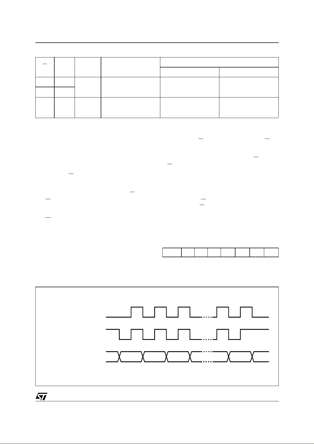
Table 3. Write Protection Control
SRWD
W
Bit
Mode Status Register
M35080
Data Bytes
Protected Area Unprotected Area
0 or 1 0 Software
11
01
Protected
(SPM)
Hardware
Protected
(HPM)
Writeable (if the WREN
instruction has set the
WEL bit)
Hardware write protected
(though not to the WIP and WEL bits, which are
set or reset by the device’s internal logic).
Bit 7 of the status register (as shown in Table 4) is
the Status Register Write Disable bit (SRWD).
When this is set to 0 (its initial delivery state) it is
possible to write to the status register if the WEL
bit (Write Enable Latch) has been set by the
WREN instruction (irrespective of the l evel being
applied to the W
input).
When bit 7 (SRWD) of the status reg ister is set to
1, the ability to write to the status register depends
on the logic level being presented at pin W
pin is high, it is possible to write to the sta-
–If W
:
tus register, after having set the WEL bit using
the WREN instruction (Write Enable Latch).
–If W
pin is low, any attempt to modify the status
register is ignored by the device, even if the
WEL bit has been set. As a consequence, all the
data bytes in the EE PROM area, protected by
the BP1 and BP0 bits of the status register, are
also hardware protected against data corruption, and appear as a Read Only EEPROM area
for the microcontroller. This mode is called the
Hardware Protected Mode (HPM).
Software write protected
by the BP0 and BP1 bits
of the status register
Hardware write protected
by the BP0 and BP1 bits
of the status register
Writeable (if the WREN
instruction has set the
WEL bit)
Writeable (if the WREN
instruction has set the
WEL bit)
It is possible to enter the Hardware Protected
Mode (HPM) either by s etting the SRWD bi t after
pulling low the W
pin, or by pulling low the W pin
after setting the SRWD bit.
The only way to abort the Hardware Protected
Mode, once entered, is to pull high the W
pin is permanently t ied to the hi gh level, the
If W
pin.
Hardware Protected Mode is never activated, and
the memory device only allows the user to protect
a part of the memory, using the BP1 and BP0 bits
of the status register, in the Software Protected
Mode (SPM).
IMPORTANT: if W pin is left floating, not driven by
the application, W
is read as a logical ’0’.
Table 4. Status Register Format
b7 b0
SRWD UV X INC BP1 BP0 WEL WIP
Note: 1. BP0, BP1: Read and wri te bits
2. UV, INC, WEL, WIP: Read only bits.
3. SRWD: Read and Write bit.
Figure 3. Dat a and Clock Timi ng
CPOL
CPHA
0
1
0
1
C
C
D or Q
MSB LSB
AI01438
3/18
M35080
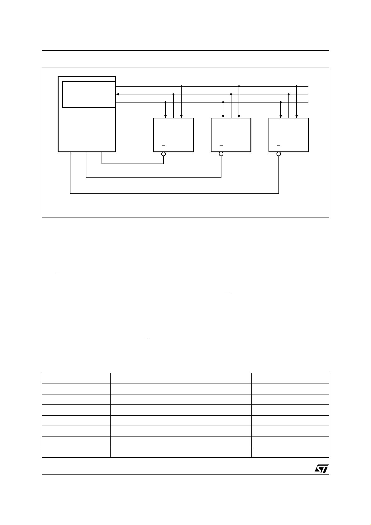
Figure 4. EEPR OM and SPI Bus
SPI Interface with
(CPOL, CPHA) =
('0', '0') or ('1', '1')
Master
(ST6, ST7, ST9,
ST10, Others)
CS3 CS2 CS1
D
Q
C
CQD
M35xxx
S
OPERATIONS
All instructions, addresses and data are shifted serially in and out of the chip (along the bus, as
shown in Figure 4). The most significant bit is presented first, with the data input (D) sampled on the
first rising edge of the clock (C) after the chip se-
) goes low (as shown in Figure 5, Figure 9,
lect (S
and Figure 12).
Every instruction, as summarized in Table 5, starts
with a single -byte cod e. If an invalid instructio n is
sent (one not contained in Table 5), the chip automatically deselects itself.
The instruction code is entered via the data input
(D), and latched on the rising edge of the clock input (C). To enter an instruction code, the device
must have been previously selected (S
held low).
CQD
M35xxx
S
CQD
M35xxx
S
AI02148C
Protection of the First 32 Bytes
The first 32-byte page is organized as 16 words
(two bytes each). The initial content of each word
on this page is 0000h. When writing to byt e-pair, a
logic comparator verifies that the new two-byte
value is larger than the val ue currently stored. If
the new value is sm aller than the current on e, no
operation is performed. It is impossible to write a
value lower than the previous one, irrespective of
the state of W
pin and status register, as indicated
in Table 6.
Write Enable (WREN) and Write Disable (WRDI)
The write enable latch, inside the memory device,
must be set prior to each WRITE and WRSR operation. The WREN instruction (write enable) sets
this latch, and the WRDI instruction (write disable)
resets it.
Table 5. Instruction Set
Instruction Description Instruction Format
WREN Set Write Enable Latch 0000 0110
WRDI Reset Write Enable Latch 0000 0100
RDSR Read Status Register 0000 0101
WRSR Write Status Register 0000 0001
READ Read Data from Memory Array 0000 0011
WRITE Write Data to Memory Array 0000 0010
WRINC Write Data to Secure Array 0000 0111
4/18
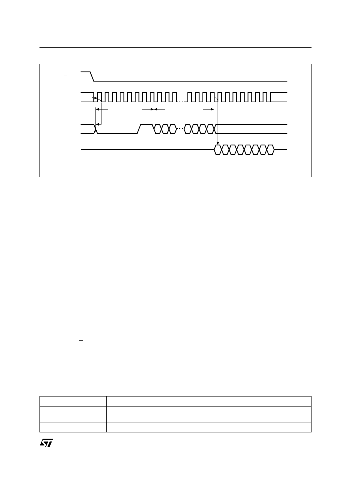
Figure 5. Rea d EEPRO M Arr a y Oper a t ion Sequence
S
21 345678910 2021222324252627
0
C
INSTRUCTION 16 BIT ADDRESS
15
D
1413 3210
M35080
28 29 30
HIGH IMPEDANCE
Q
Note: 1. The most signific ant address bi ts, A15-A 10, are treated as Don’t Care.
The latch becomes reset by any of the f ollowing
events:
– Power on
– WRDI instruction completion
– WRSR in s t ru ctio n completio n
– WRITE instruction completion.
As soon as the WREN or WRDI instruction is re-
ceived, the memory device first executes the instruction, then enters a wait mode until the device
is deselected.
Read Status Register (RDSR)
The RDSR instruction allows the status register to
be read, and can be sent at any time, even during
a Write operation. Indeed, when a Write is in
progress, it is recommended th at the value of t he
Write-In-Progress (WIP) bit be checked. The value
in the WIP bit (whose position in the status register
is shown in Table 4) can be continuously p olled,
before sending a new WRITE instruction. This can
be performed in one of two ways:
■ Repeated RDSR instructions (each one
consisting of S
being taken low, C being clocked
8 times for the instruction and 8 times for the
read operation, and S
being taken high)
■ A single, prolonged RDSR instruction
(consisting of S
clocked 8 times for the instruction and kept
running for repeated read operations), as
shown in Figure 6.
The Write-In-Process (WIP) bit is read-only, and
indicates whether the memory is busy with a Write
operation. A ’1’ indicates that a write is in progress,
and a ’0’ that no write is in progress.
The Write Enable Latch (WEL) bit indicates the
status of the write enable latch. It, too, is read-only.
Its value can only be changed by one of the events
listed earlier, or as a result of executing WREN or
WRDI instruction. It cannot be changed using a
WRSR instruction. A ’1’ i ndicates that the latch is
set (the forthcoming Write instruction will be executed), and a ’0’ that it is reset (and any forthcoming Write instructions will be ignored).
The Block Protect (BP0 and BP1) bits indicate the
amount of the memory that is to be write-protected. These two bits are non-volatile. They are set
using a WRSR instruction.
During a Write operation (whether it be to the
memory area or to the status register), all bits of
the status register remain valid, and can be read
using the RDSR instruction. However, during a
Write operation, the values of the no n-vo latile bits
DATA OUT
765432 0
MSB
1
being taken low, C being
AI01793
Table 6. Memory Mapping
Address Protection
000h-01Fh
020h-3FFh No specific protection except the one as of Table 7
Incremental area: a word (2 bytes) can be written only if the new value to write is larger
than the value already stored
5/18
M35080
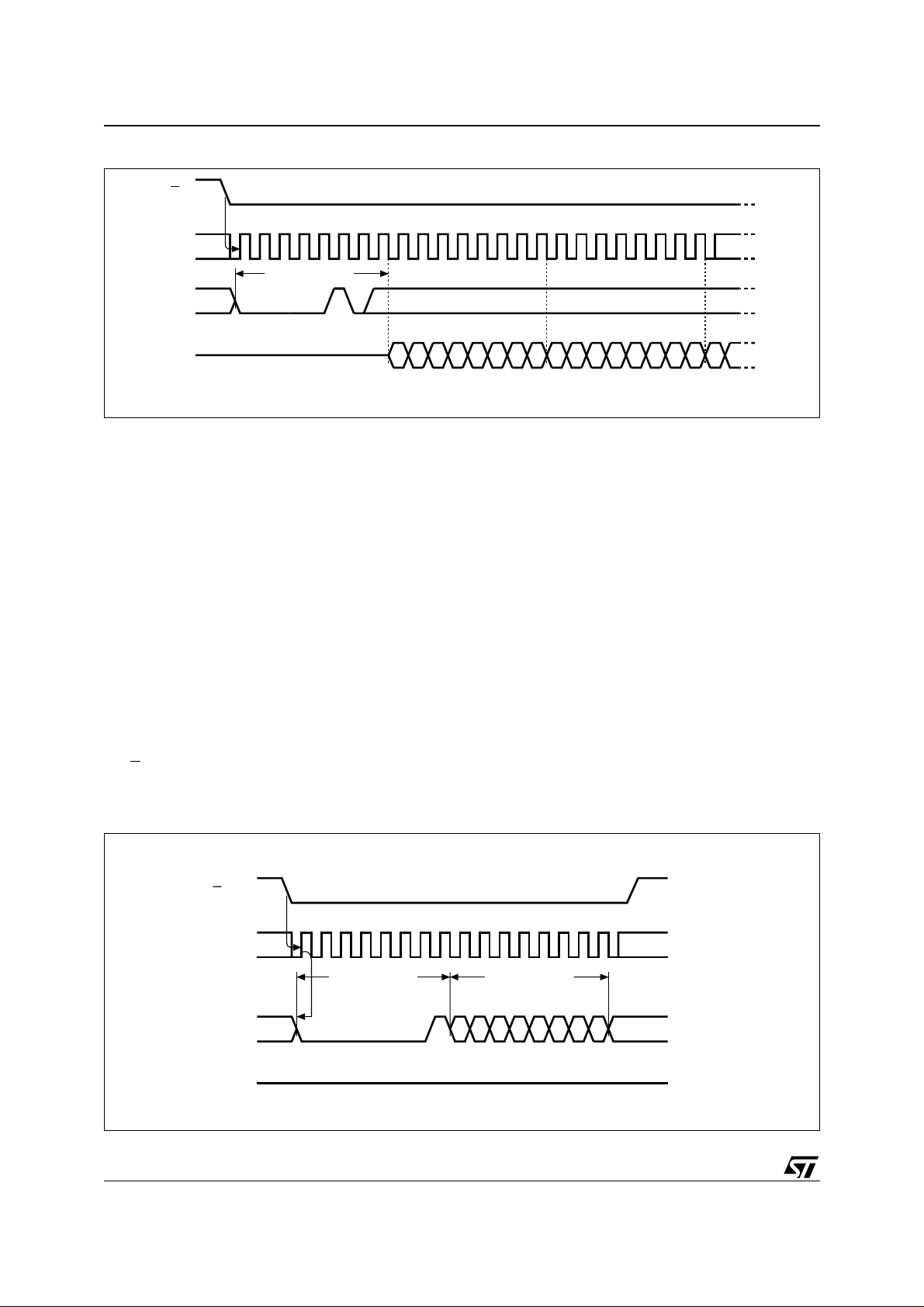
Figure 6. RDSR: Read Status Register Sequence
S
21 3456789101112131415
0
C
INSTRUCTION
D
Q
HIGH IMPEDANCE
STATUS REG. OUT
7 6543210
MSB
(SRWD, BP0, BP1) be come frozen at a constant
value. The updated value of these bi ts becomes
available when a new RDSR instruction is executed, after completion of the write cycle. On the other hand, the two read-only bits (WEL, WIP) are
dynamically updated during internal write cycles.
Using this facility, it is possible to poll the WIP bit
to detect the end of the internal write cycle.
The Comparator bit (INC) indicates if the new val-
ue written in the 16 first word is lower ‘1’ or higher
‘0’ than the previous stored value.
The UV bit indicates if the memory chip has been
erased.
Write Status Register (WRSR)
The format of the WRSR instruction is shown in
Figure 7. After the instruction and the eigh t bits of
the status register have been latched-in, the internal Write cycle is triggered by the rising edge of
line. This must occur after the falling edge of
the S
STATUS REG. OUT
the 16
the 17
7 6543210
MSB MSB
th
clock pulse, and before the rising edge of
th
clock (as indicated in Figure 7), otherwise
7
AI02031
the internal write sequence is not performed.
The WRSR instruction is used for the following:
■ to select the size of memory area that is to be
write-protected
■ to select between SPM (Software Protected
Mode) and HPM (Hardware Protected Mode).
The size of the write-protection area applies equally in SPM and HPM. The BP 1 and BP0 b its of the
status register have the appropriate value (see Table 7) written into them after the contents of the
protecte d ar ea of t he EEPROM have been written.
The initial delivery state of the BP1 and BP0 bits is
00, indicating a write-protection size of 0.
Figure 7. WRSR: Write Status Register Sequence
S
21 3456789101112131415
0
C
INSTRUCTION STATUS REG.
D
MSB
HIGH IMPEDANCE
Q
6/18
765432 0
1
AI01797
 Loading...