

®
M34S32
32K Serial I2C Bus EEPROM
With User-Defined Read-Only Block and 32-Byte OTP Page
PRELIMINARY DATA
■ TWO WIRE I
2
C SERIAL INTERFACE,
SUPPORTS 400kHz PROTO COL
■ COMPATIBLE WITH I
2
C EXTENDED
ADDRESSING
■ 1 MILLION ERASE/WRITE CYCLES
■ 40 YEARS DATA RETENTION
■ SINGLE SUPPLY VOLT AG E
■ HARDWARE WRITE CONTROL
■ USER-DEFINED READ-ONLY BLOCK
■ 32 BYTES OTP PAGE
■ BYTE and PAGE WRITE (up to 32 BYTES)
■ BYTE, RANDOM and SEQUENTIAL READ
MODES
■ SELF TIMED PROGRAMING CYCLE
■ AUTOMATIC ADDRESS INCREMENTING
■ ENHANCED ESD and LATCH-UP
PERFORMANCES
DESCRIPTION
The M34S32 is a 32K bit electrically erasable programmable memory (EEPROM), organized as
4096 x 8 bits.
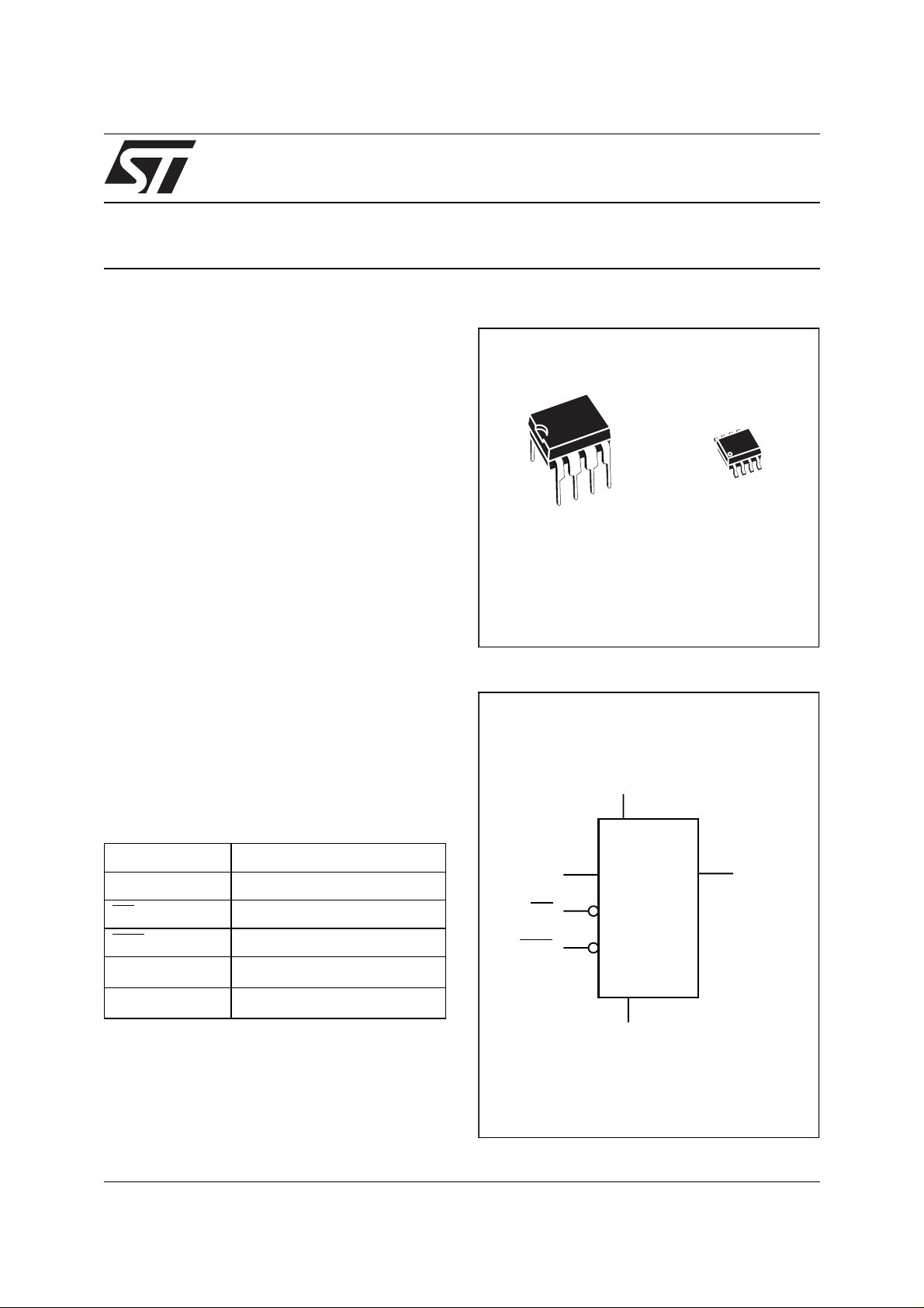
Figure 1. Delivery Forms
8
1
PSDIP8 (BN)
0.25 mm Frame
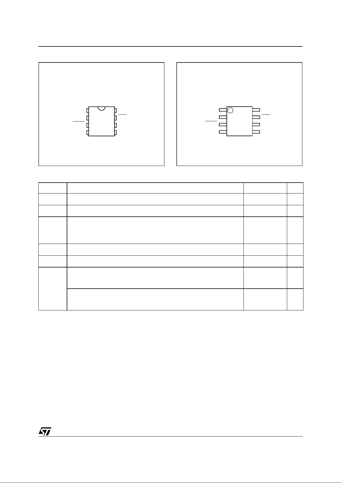
Figure 2. Logic Diagram
V
CC
8
1
S08 (MN)
150 mil Width
Table 1. Signal Names
SDA Serial Data Address Input/Output
SCL Serial Clock
WC
WCR
Write Control of Control Register
V
CC
V
SS
This is a Preliminary Data. Details are subject to change without notice.
Write Control
Supply Voltage
Ground
SCL
WC
WCR
M34S32
V
SS
SDA
AI02468
1/18June 1998
M34S32
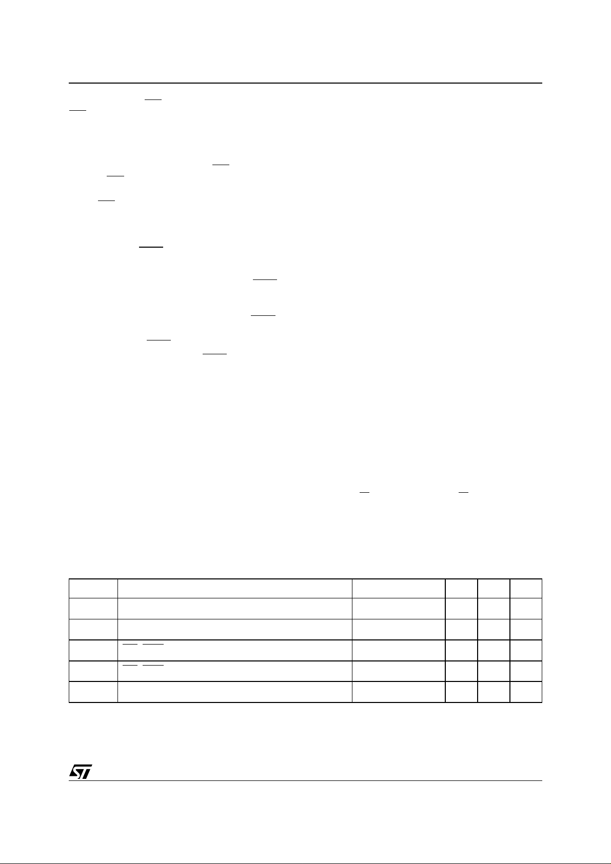
Figure 3. DIP Pin Connections
M34S32
1
NC V
2
SS
3
4
WCR
8
7
6
5
AI02448
CC
WCNC
SCL
SDAV
Table 2. Absolute Maximum Ratings
(1)
Figure 4. SO Pin Connections
M34S32
NC V
1
2
WCR
SS
3
4
8
7
6
5
AI02449
CC
WCNC
SCL
SDAV
Symbol Parameter Value Unit
T
T
A
STG
Ambient Operating Temperature –40 to 125 °C
Storage Temperature –65 to 150 °C
Lead Temperature, Soldering (SO8 package) 40 sec 215 °C
T
LEAD
(PSDIP8
package)
10 sec 260 °C
V
IO
V
CC
Input or Output Voltages –0.6 to 6.5 V
Supply Voltage –0.3 to 6.5 V
(Human Body model)
Electrostatic Discharge Voltage
V
ESD
Electrostatic Discharge Voltage
Note: 1. Except for the ra ting “Op era ting T em perat ure Ra nge ”, s tresse s abov e tho se lis ted in t he Tab le “ A bsolut e M axi mum R ati ngs”
may cause perm ane nt damag e to th e devic e. T hese ar e str ess ra tin gs only and o perat ion of t he de vice at thes e or any other
conditions above those indi cated in th e Operating section s of this specification is not implied. E xposure to Absolut e M aximum
Rating conditions for extended periods may a ffect device r eliability. R efer a lso to the STMicroelectronics SURE Program and
other relevant quality documents.
1. MIL-STD-883C, 3015.7 (100 pF,
1500 Ω)
(Machine model)
2. EIAJ IC-121 (Condition C)
(200 pF, 0 Ω)
4000 V
500 V
2/18

M34S32
DESCRIPTION (cont’d)
2
The memory is compatible with t he I
C extended
addressing standard, two wire serial interface
which uses a bi-directional data bus and serial
clock. The memory carries a built-in 4 bit, unique
device identification code (1010) corresponding to
2
the I
C bus definition. The memory behaves as
slave devices in the I
2
C protocol with all memory
operations synchronized by the serial clock. Read
and write operations are initiated by a START condition generated by the bus m aster. The START
condition is followed by the Device Select Byte.
This is a stream o f 4 bits (the identification c ode
1010), then 3 bits o f memory block access input,
plus one read/write bit. The byte is finally terminated by an acknowledge bit.
The M34S32 contains three memory blocks: the
OTP page, the EEPROM block and the ROM
block. The OTP (One T ime Programmab le) page
is a page of 32 bytes, written once by the user. The
OTP page is not located within the 32 Kbits EEPROM area. Once written, the OTP page cannot be
modified by further write instructions. The ROM
block resides inside the 32 Kbit EEPROM area.
The size of the ROM block is defined (by the user)
with the help of the Control Register.
The OTP page is accessed with the Device Select
Byte 1010001x, the EEPROM and ROM blocks
are accessed with the Device Select Byte
1010000x. The con trol register is accessed with
the Device Select Byte 1010100x (see Table 3).
Table 3. Device Select Byte
When writing data to the memory it responds to
the 8 bits received by asserting an acknowledge
bit during the 9th bit time. When data is read by the
bus master, it acknowledges the receipt of the
data bytes in the same way.
Data transfers are terminated with a STOP condi tion.
Power On Reset: VC C lock out wri te protect. In
order to prevent data corrup tion and inadvertent
write operations during power up, a Power On Reset (POR) circuit is implemented. Until the VCC
voltage has reached the POR threshold value, the
internal reset is active: all operations are disabled
and the device will not respon d to any comma nd.
In the same way, when VCC drops down from the
operating voltage to below the POR threshold value, all operations are disabled and the device will
not respond to any command. A stable VCC must
be applied before applying any logic signal.
SIGNAL DESCRIPTION
Serial Clock (SCL). Th e SC L input pin is used to
synchronize all data in and out of the memory. A
resistor can be connected from the SCL line to
VCC to act as a pull up (see Figure 3)
Serial Data (SDA). The SDA pin is bi-directional
and is used to transfer data in or out of the memory. It is an open drain output that may be wire-
OR’ed with other open drain or open collector signals on the bus. A pull-up resistor must be connected from the SDA bus line to V
(see Figure
CC
3).
Device Code Memory Block Access RW
Device Select Bit b7 b6 b5 b4 b3 b2 b1 b0
EEPROM and ROM access 1 0 1 0 0 0 0 RW
OTP Page access 1 0 1 0 0 0 1 RW
Control Register access 1 0 1 0 1 0 0 RW
Table 4. Operating Modes
Mode RW bit
Current Address Read 1 1 START, Device Select, RW
0
Random Address Read
1 reSTART, Device Select, RW
Sequential Read 1 ≥ 1 As CURRENT or RANDOM Mode
Byte Write 0 1 START, Device Select, RW
Page Write 0 ≤ 32 START, Device Select, RW
3/18
Data
Bytes
1
Initial Sequence
START, Device Select, RW
= 1
= 0, Address
= 1
= 0
= 0
M34S32
Write Control (WC). The Write Control feature
is useful to protect the conte nts of the whole
WC
EEPROM area from any erroneous erase/write cycle. It also protects the OTP page ag ainst the first
write attempt. The Write Control signal polarity can
be selected with the WCpol bit of the Control Register (see Table 13). When pin WC
ed, the WC
input is internally read as VIL (see
is unconnect-
Table 5).
When WC
and WCpol are activating the Write Protection, Device Select and Address byte s are acknowledged; Data bytes are not acknowledged
(see Figure 11).
Write Control (WCR
). In order to prevent spurious
writes to the Control Regi ster, the user can also
make the Control Register Read Only (Write is inhibited). This is achieved by use of the WCR
pin
and the CRWD bit (see Table 14) :
– - if CRWD b it = 0, the Control register can be
modified regardless of the state of the WCR
pin.
– - if CRWD bit = 1, the C ontrol register can be
modified if the WCR
– - i f CRWD bit = 1 and the WCR
pin is high.
pin is low, the
Control Register is Write Protected.
DEVICE OPERATION
2
C Bus Background
I
The memory supports the extended addressing
2
I
C protocol. This protocol defines any device that
sends data onto the bus as a t ransmitter and any
device that rea ds the data as a rec eiver. The de vice that controls the data transfer is known as the
master and the other as the slave. The master will
always initiate a data transfer and will provide the
serial clock for synchronisation. The memory is always a slave device in all communications.
Start Condition. START is identified by a high to
low transition of the S DA line while the clock SCL
is stable in the high state. A START condition must
precede any command for data transfer. E xcept
during a programming cycle , the memory con ti n uously monitors the SDA and SCL signals for a
START condition and will not respond unless one
is given.
Stop C ondition. STOP is identified by a low to
high transition of the SDA line while the clock SCL
is stable in the high state. A STOP condition terminates communication between the memory and
the bus master. A STO P c ondi tion at the end of a
Read command forces the stand-by state. A
STOP condition at the end of a Write command
triggers the internal EEPROM write cycle.
Acknowledge Bit (ACK). An ac knowled ge s ignal
is used to indicate a successful data transfer. The
bus transmitter, either master or slave, will release
the SDA bus after send ing 8 bits of data. During
the 9th clock pulse the receiver pulls the SDA bus
low to acknowledge the receipt of the 8 bits of data.
Data Input. During data input the memory samples the SDA bus signal on the rising edg e of the
clock SCL. For correct device operation the SDA
signal must be stable during the clock low to high
transition and the data must c hange ONLY when
the SCL line is low.
Device Selection. To start communication between the bus master an d the slav e memory , the
master must initiate a START condition. The 8 bits
sent after a START condition are made up of a Device Select Byte of 4 bits that identifie s the devi ce
type, 3 memory block access bits and one bit for a
READ (RW
= 1) or WRITE (RW = 0) operation.
There are two modes both for read and write.
These are summarised in Table 4 and described
hereafter. Communication between the master
and the slave is ended with a STOP condition.
(1)
Table 5. Input Parameters
(T
= 25°C, f = 400 kHz)
A
Symbol Parameter Test Condition Min. Max. Unit
C
C
Z
Z
t
LP
Note: 1. Sampled only, not 100% tested in production.
Input Capacitance (SDA) 8 pF
IN
Input Capacitance (other pins) 6 pF
IN
WC, WCR Input Impedance
L
WC, WCR Input Impedance
H
Low-pass filter input time constant (SDA and SCL) 100 ns
V
IN
V
IN
≤ 0.3 V
≥ 0.7 V
CC
CC
520kΩ
500 kΩ
4/18

Figure 5. Maximum RL Value versus Bus Capacitance (CBUS) for an I2C Bus
V
20
16
12
8
Maximum RP value (kΩ)
4
0
10 1000
C
BUS
fc = 400kHz
100
(pF)
fc = 100kHz
CC
MASTER
SDA
SCL
R
L
C
M34S32 -
R
L
BUS
AI01665
C
BUS
Table 6. DC Characteristics (T
= 0 to 70°C, –40 to 85°C; VCC = 4.5V to 5.5V, 2.5V to 5.5V)
A
Symbol Parameter Test Condition Min. Max. Unit
I
LI
I
LO
I
CC
I
CC1
I
CC2
V
IL
V
IH
V
IL
V
IH
V
OL
Input Leakage Current (SCL,
SDA)
Output Leakage Current
Supply Current
Supply Current (W series)
Stand-by Current
Stand-by Current (W series)
Input Low Voltage (WC
Input High Voltage (WC
, WCR) – 0.3 0.5 V
, WCR)
0 ≤ VIN ≤ V
0 ≤ V
V
CC
CC
≤ VCC; SDA in Hi-Z
OUT
= 5 V; fC = 400 kHz
(rise/fall time < 30 ns)
V
= 2.5 V; fC = 400 kHz
CC
(rise/fall time < 30 ns)
VIN = VSS or VCC ; VCC = 5 V
= VSS or VCC ; VCC = 2.5 V
V
IN
Input Low Voltage (other pins) – 0.3
Input High Voltage (other pins)
= 3 mA, VCC = 5 V
Output Low Voltage
Output Low Voltage (W series)
I
OL
= 2.1 mA, VCC = 2.5 V
I
OL
±2 µA
±2 µA
2 mA
1 mA
10 µA
2 µA
- 0.5 VCC + 1
V
CC
0.3 VCC
0.7 VCC VCC + 1
0.4 V
0.4 V
V
V
V
5/18
M34S32
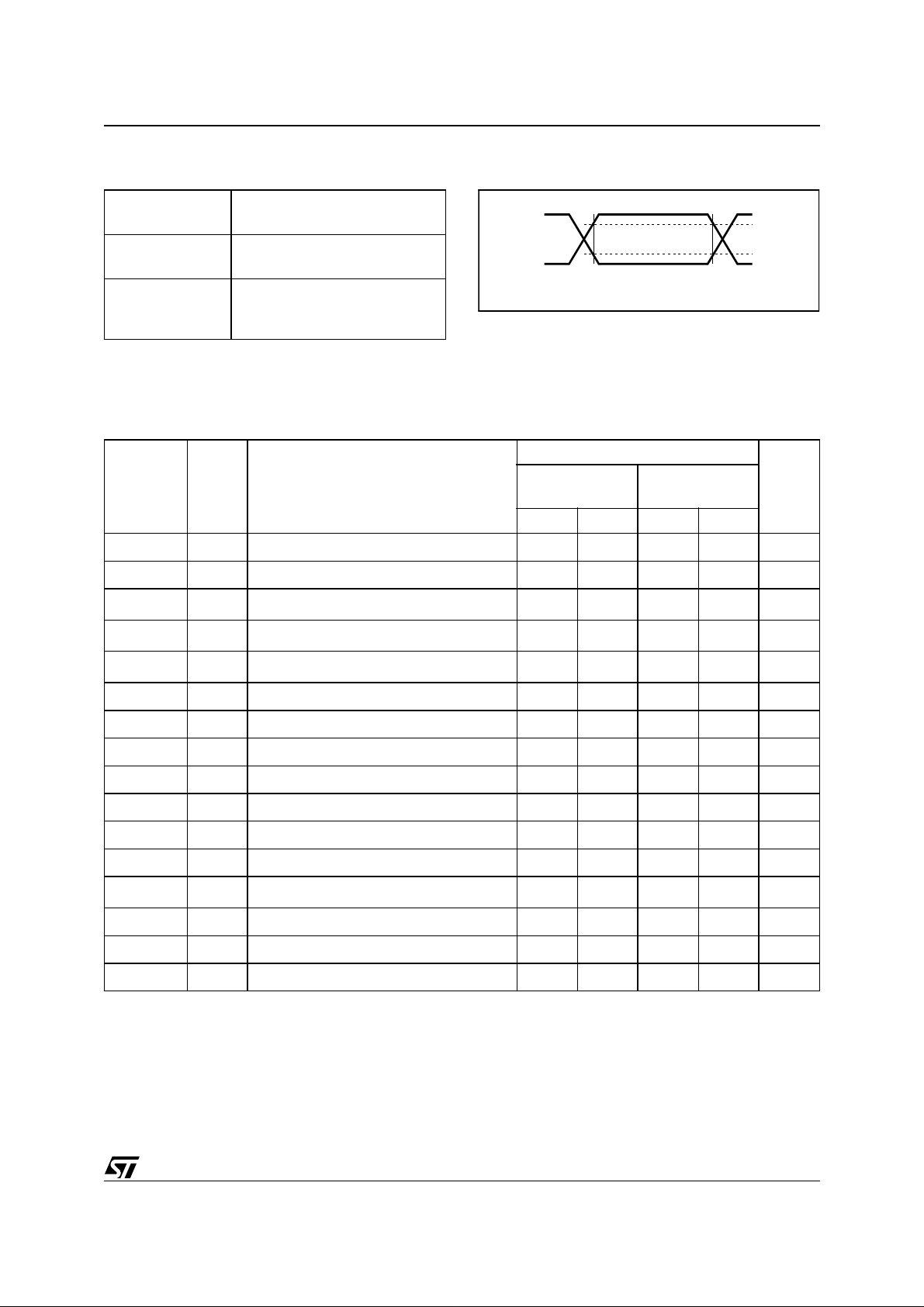
Table 7. AC Measurement Conditions
Input Rise and
Fall Times
Input Pulse
Voltages
≤ 50ns
0.2 V
to 0.8 V
CC
CC
Figure 6. AC Testing Input/Output Waveforms
0.8V
CC
0.2V
CC
Input and Output
Timing Reference
0.3 V
to 0.7 V
CC
CC
Voltages
Table 8. AC Characteristics (TA = 0 to 70 °C,
–40 to 85°C; V
Symbol Alt. Parameter
t
CH1CH2
t
CL1CL2
t
t
t
t
t
t
t
t
t
t
t
t
f
t
Note: 1. Sampled only, not 100% tested in production.
(1)
DH1DH2
(1)
DL1DL2
(2)
CHDX
CHCL
DLCL
CLDX
CLCH
DXCX
CHDH
DHDL
(3)
CLQV
QLQx
C
W
2. For a reS T AR T condition , or following a write cy cle.
3. The minimum value delays the falling/rising edge of SDA away from SCL=1 in order to avoid unwanted START and/or STOP
conditio ns .
= 4.5V to 5.5V, 2.5V to 5.5V)
CC
t
Clock Rise Time 300 300 ns
R
t
Clock Fall Time 300 300 ns
F
t
SDA Rise Time 20 300 20 300 ns
R
t
SDA Fall Time 20 300 20 300 ns
F
t
SU:STA
t
HIGH
t
HD:STA
t
HD:DAT
t
t
SU:DAT
t
SU:STO
t
f
t
LOW
BUF
t
AA
t
DH
SCL
WR
Clock High to Input Transition 600 600 ns
Clock Pulse Width High 600 600 ns
Input Low to Clock Low (START) 600 600 ns
Clock Low to Input Transition 0 0 µs
Clock Pulse Width Low 1300 1300 ns
Input Transition to Clock Transition 100 100 ns
Clock High to Input High (STOP) 600 600 ns
Input High to Input Low (Bus Free) 1300 1300 ns
Clock Low to Next Data Out Valid 200 900 200 900 ns
Data Out Hold Time 200 200 ns
Clock Frequency 400 400 kHz
Write Time 10 10 ms
M34S32
V
= 4.5V to
CC
5.5V
VCC = 2.5V to
5.5V
Min. Max. Min. Max.
0.7V
0.3V
AI00825
Unit
CC
CC
6/18
 Loading...