

SGS Thomson Microelectronics M34D64 Datasheet
M34D64
M34D32
64/32 Kbit Serial I²C Bus EEPROM
With Hardware Write Control on Top Quarter of Memory
PRELIMINARY DATA
■ Compat ible with I
■ Two Wire I
2
C Extended Addressing
2
C Serial Interface
Supports 400 kHz Protocol
■ Single Supply Voltage:
– 4.5V to 5.5V for M34Dxx
– 2.5V to 5.5V for M34Dxx-W
– 1.8V to 3.6V for M34Dxx-R
■ Hardware Write Control of the top quarter of
memory
■ BYTE and PAGE WRITE (up to 32 Bytes)
■ RANDOM and SEQUENTIAL READ Modes
■ Self-Tim e d P ro g r amming Cycle
■ Automatic Address Incrementing
■ Enhanced ESD/Latch-Up Behavior
■ More than 1 Million Erase/Write Cycles
■ More than 40 Year Data Retention
DESCRIPTION
These electrically erasable programmable
memory (EEPROM) devices are fabricated with
STMicroelectronics’ High Endurance, CMOS
technology. This guarantees an endurance
typically well above one million Erase/Write
cycles, with a data retention of 40 years. The
memories are organized as 8192x8 bits (M34D64)
and 4096x8 bits (M34D32), and operate down to
8
1
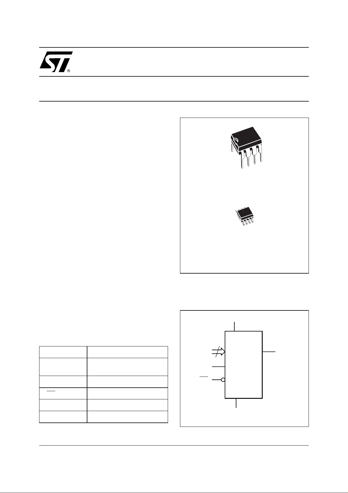
PSDIP8 (BN)
0.25 mm frame
8
1
SO8 (MN)
150 mil width
Figure 1. Logic Diagram
V
CC
Table 1. Signal Names
E0, E1, E2 Chip Enable Inputs
SDA Serial Data/Address Input/
Output
SCL Serial Clock
WC
V
CC
V
SS
May 2000
This is preliminary information on a new product now in development or undergoing evaluation. Details are subject to change without notice.
Write Control
Supply Voltage
Ground
E0-E2 SDA
SCL
WC
3
M34D64
M34D32
V
SS
AI02850
1/15
M34D64, M34D32
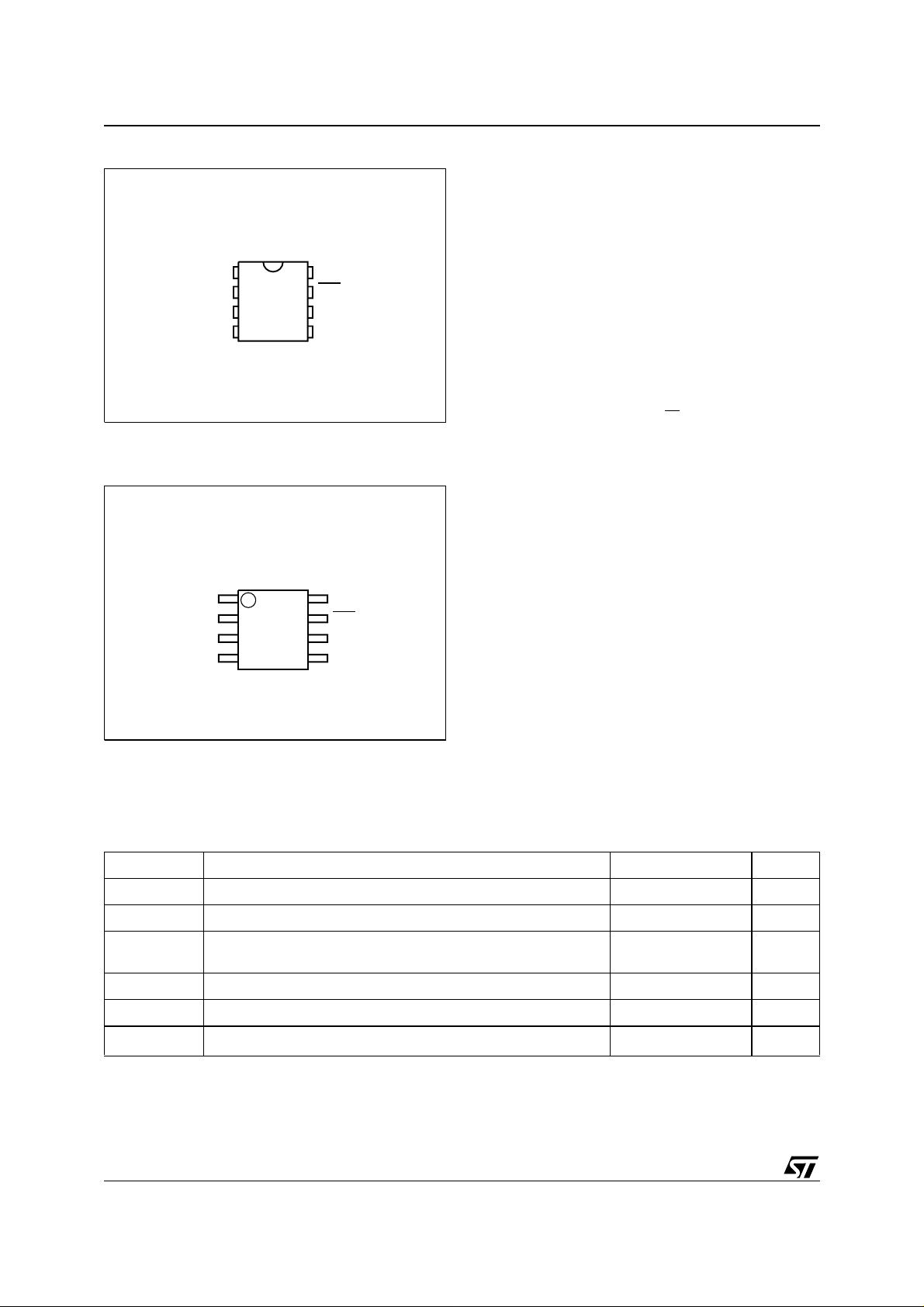
Figure 2A. DIP Connections
M34D64
M34D32
1
E0 V
2
3
E2
4
SS
8
7
6
5
AI02851
Figure 2B. SO C on ne ct i on s
M34D64
M34D32
E0 V
1
2
E2
SS
3
4
8
7
6
5
AI02852
CC
WCE1
SCL
SDAV
CC
WCE1
SCL
SDAV
2.5 V (for the -W version of each device), and
down to 1.8 V (for the -R version of each device).
The M34D64 and M34D32 are available in Plastic
Dual-in-Line and Plastic Small Outline packages.
These memory devices are compatible with the
2
C extended memory standard. This is a two wire
I
serial interface that uses a bi-directiona l data bus
and serial clock. The memory carries a built-in 4bit unique Device Type Identifier code (1010) in
accordance with the I
The memory behaves as a slave device in the I
2
C bus definition.
2
protocol, with all memory operations synchronized
by the serial clock. Read and Write operations are
initiated by a START condition, genera ted by the
bus master. The START condition is followed by a
Device Select Code and RW
bit (as described in
Table 3), terminated by an acknowledge bit.
When writing data to the memory, the memory
inserts an acknowledge bit during the 9
th
bit time,
following the bus master’s 8-bit transmission.
When data is read by the bus master, the bus
master acknowledges the receipt of t he data b yte
in the same way. Data transfers are terminated by
a STOP condition after an Ack for WRITE, and
after a NoAck for READ.
Power On Reset: V
Lock-Out Write Protect
CC
In order to prevent data corruption and inadvertent
write operations during power up, a Power On
Reset (POR) circuit is included. The internal reset
is held active until the V
voltage has reached
CC
the POR threshold value, and all operations are
disabled – the device will not respond to any
command. In the same way, when V
drops from
CC
the operating voltage, below the POR threshold
value, all operations are disabled an d the device
will not respond to any command. A stable and
C
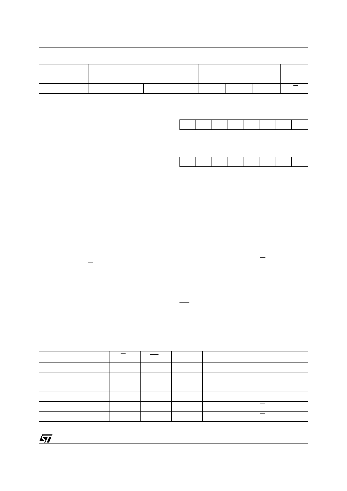
Table 2. Absolute Maximum Ratings
Symbol Parameter Value Unit
T
A
T
STG
T
LEAD
V
IO
V
CC
V
ESD Electrostatic Discharge Voltage (Human Body model)
Note: 1. Exc ept for the rating “Operating Temperature Ra nge”, stres ses above those listed in the Table “Absolute Maximum Ratings” may
2/15
cause permanent damage to the device. These are stress ratings only, and operation of the device at these or any other conditions
above those indi cated in t he Operating sect i ons of thi s specifi cation i s not impl i ed. Exposure to Absolute M aximum Rating c onditions for extended periods may affect device reliability. Refer also to the ST SURE Program and other relevant quality documents.
2. MIL -STD-883C, 3015.7 (1 00 pF, 1500 Ω)
3. EIA J I C-121 (Condition C) (200 pF, 0 Ω)
Ambient Operating Temperature -40 to 125 °C
Storage Temperature -65 to 150 °C
Lead Temperature during Soldering
Input or Output range -0.6 to 6.5 V
Supply Voltage -0.3 to 6.5 V
1
PSDIP8: 10 sec
SO8: 40 sec
2
260
215
4000 V
°C
M34D64, M34D32
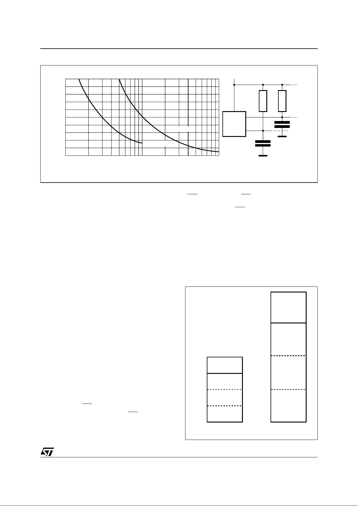
Figure 3. Maximum R
20
16
12
8
Maximum RP value (kΩ)
4
0
10 1000
Value versus Bus Capacitance (C
L
fc = 100kHz
fc = 400kHz
100
C
(pF)
BUS
valid VCC must be applied before applying any
logic signal.
SIGNAL DESCRIPTION
Serial Clock (SCL)
The SCL input pin is used to strobe all data in and
out of the memory. In applications where this line
is used by slaves to synchronize the bus to a
slower clock, the master must have an open drain
output, and a pull-up resistor must be c onnected
from the SCL line to V
. (Figure 3 indicates how
CC
the value of the pull-up resistor can be calculated).
In most applications, though, this method of
synchronization is not employed, and so the pullup resistor is not necessary, provided that the
master has a push-pull (rather than open drain)
output.
Serial Data (SDA)
The SDA pin is bi-directional, and is used to
transfer data in or out of the memory. It is an open
drain output that may be wire-OR’ed with other
open drain or open collector signals on the bus. A
pull up resistor must be connected f rom the SDA
bus to V
. (Figure 3 indicates how t he value of
CC
the pull-up resistor can be calculated).
Chip Enable (E2, E1, E0)
These chip enable inputs are used to set the value
that is to be looked for on the three least significant
bits (b3, b2, b1) of the 7-bit device select code.
These inputs must be tied to V
or VSS to
CC
establish the device select code.
Write Control (WC
The hardware Write Control pin (WC
)
) is useful for
protecting the top quarter of the memory (as
shown in Figure 4) from inadvertent erase or write.
The Write Control signal is used to enable
) for an I2C Bus
BUS
V
CC
R
SDA
MASTER
=VIL) or disable (WC=VIH) write instructions to
(WC
SCL
R
C
BUS
L
C
BUS
AI01665
L
the top quarter of the memory area. When
unconnected, the WC
V
, and write operations are allowed.
IL
input is internally read as
DEVICE OPERATION
2
The memory device supports the I
C protocol.
This is summarized in Figure 5, and is compared
with other serial bus protocols in Application Note
AN1001
. Any device that sends data on to the bus
is defined to be a transm itter, and any device that
Figure 4. Me m ory Map of Write C ont rol Areas
1FFh
Write Controlled
Area
180h
FFh
Write Controlled
C0h
80h
40h
00h
Area
M34D32
100h
80h
000h
M34D64
AI03114
3/15
M34D64, M34D32
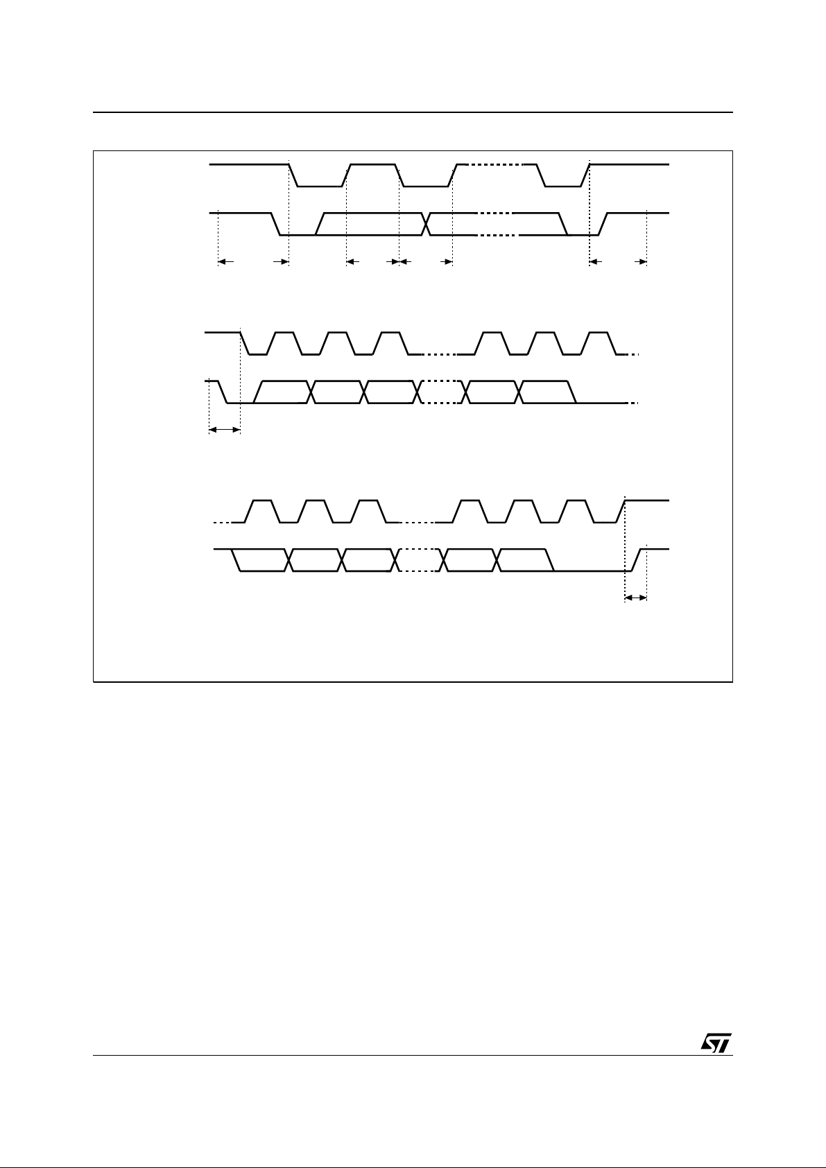
2
Figure 5. I
C Bus Protocol
SCL
SDA
SCL
SDA
SCL
SDA
START
CONDITION
START
CONDITION
SDA
INPUT
1 23 789
MSB
1 23 789
MSB ACK
SDA
CHANGE
CONDITION
ACK
STOP
STOP
CONDITION
reads the data to be a receiver. The device that
controls the data transfer is k nown as the master,
and the other as the slave. A data transfer can only
be initiated by the mas ter, which wi ll also provide
the serial clock for synchronization. The memory
device is always a slave device in all
communication.
Start Condition
START is identified by a high t o low transition of
the SDA line while the clock, SCL, is s table i n t he
high state. A START condition must precede any
data transfer command. The memory device
continuously monitors (except during a
programming cycle) the SDA and SCL lines for a
START condition, and will not respond unless one
is given.
Stop Condition
STOP is identified by a low to high transition of the
SDA line while the clock SCL is stable in the high
4/15
AI00792
state. A STOP condition terminates
communication between the m emory device and
the bus master. A STOP condition at the end of a
Read command, after (and only after) a NoAck,
forces the memory device into its standby state. A
STOP condition at the end of a Write com mand
triggers the internal EEPROM write cycle.
Acknowledge Bit (ACK)
An acknowledge signal is used to indicate a
successful byte transfer. The bus transmitter,
whether it be master or slave, releases the SDA
bus after sending eight bits of data. During the 9
clock pulse period, the receiver pulls the SDA bus
low to acknowledge the receipt of the eight data
bits.
Data Input
During data input, the memory device samples the
SDA bus signal on the rising edge of the clock,
SCL. For correct device operation, the SDA signal
must be stable during the clock low-to-high
th
M34D64, M34D32
Table 3. Device Select Code
b7 b6 b5 b4 b3 b2 b1 b0
Device Select Code 1 0 1 0 E2 E1 E 0 RW
Note: 1. The most significant bit, b7, is sent firs t.
transition, and the data must change
the SCL line is low .
Memory Addressing
To start communication betwee n the bus master
1
Device Type Identifier Chip Enable RW
only
when
Table 4. Most Significant Byte
b15 b14 b13 b12 b11 b10 b9 b8
Note: 1. b15 to b13 are Don’ t Care on the M34D64 series.
b15 to b12 are Don’t Care on the M34D3 2 series.
and the slave memory, the master must initiate a
START condition. Following this, the master sends
the 8-bit byte, shown in Table 3, on the SDA bus
line (most significant bit first). This consists of the
Table 5. Least Significant Byte
b7 b6 b5 b4 b3 b2 b1 b0
7-bit Device Select Code, and the 1-bit Read/Write
Designator (RW). The Device Select Code is
further subdivided into: a 4-bit Device Type
Identifier, and a 3-bit Chip Enable “Address” (E2,
E1, E0 ) .
To address the memory array, the 4-bit Device
Type Identifier is 1010b.
If all three chip enable inputs are connected, up to
eight memory devices can be connected on a
single I
2
C bus. Each one is given a unique 3-bit
code on its Chip Enable inputs. When the Device
Select Code is received on the SDA bus, the
memory only responds if t he Chip Select Code is
the same as the pattern applied to its Chip Enable
pins.
th
The 8
bit is th e RW bit. This is set to ‘1’ for read
and ‘0’ for write operations. If a match occurs on
the Device Select Code, the corresponding
memory gives an acknowledgment on the SDA
bus during the 9
th
bit time. If the memory does not
match the Device Sel ect Code, it deselects itself
from the bus, and goes into stand-by mode.
There are two modes both for read and write.
These are summarized in Table 6 and described
later. A communication between the m aster and
the slave is ended with a STOP condition.
Each data byte in the m emory has a 16-bit (two
byte wide) address. The Most Significant Byte
(Table 4) is sent first, followed by the Least
significant Byte (Table 5). B its b15 to b0 form the
address of the byte in memory. Bits b15 to b13 are
treated as a Don’t Care bit on the M34D64
memory. Bits b15 to b12 are treated as Don’t Care
bits on the M34D32 memory.
Write Operations
Following a START con dition the ma ster sends a
Device Select Code with the RW
bit set to ’0’, as
shown in Table 6. The memory acknowledges this,
and waits for two address bytes. The memory
responds to each address byte with an
acknowledge bit, and then waits for the data byte.
Writing to the memory may be inhibited if the WC
input pin is taken high. Any write command with
WC
=1 (during a period o f time from the START
condition until the end of the two address bytes)
will not mo dify the cont ents of the top quarter of
the memo r y.
Table 6. Operating Modes
Mode RW bit
Current Address Read 1 X 1 START, Device Select, RW
Random Address Read
Sequential Read 1 X
Byte Write 0 V
Page Write 0 V
Note: 1. X = V
IH
or V
.
IL
0X
1 X reSTART, Device Select, RW
WC
1
IL
IL
Bytes Initial Sequence
1
1 Similar to Current or Random Address Read
≥
1 START, Device Select, RW = ‘0’
32 START, Device Select, RW
≤
START, Device Select, RW
= ‘1’
= ‘0’, Address
= ‘1’
= ‘0’
5/15
 Loading...