

Page 1
M34C00
3 x 128 bit Serial I²C Bus EEPROM
For ee-Tags
PRELIMINARY DATA
■ Two-Wire I
2
C Serial Interface
Supports 400 kHz Protocol
■ 2.5 V to 5.5 V Single Supply Voltage
■ 384-bit EEPROM divided in three areas:
– 128 bits of non-erasable memory
– 128 bits of standard EEPROM
– 128 bits that can be permanently Write-
protected (to behave as ROM)
■ Self-Tim e d P rogram Cyc le
■ Enhanced ESD/Latch-Up Protection
■ More than 1 Million Erase/Write Cycles
■ More than 40 Year Data Retention
DESCRIPTION
The M34C00 is a 384-bit serial EEPROM. The
bottom third of the memory area (from location 00h
to 0Fh) can be Write-protected using a specially
designed software Write-protection mechanism.
By sending the device a specific sequence, the
first 128 bits of the memory become permanently
Write-protected. Care must be taken when using
this sequence as its effect cannot be reversed.
The top third of the mem ory area (from location
20h to 2Fh) is already configured to give the
functional equivalence of a non-erasable memory.
That is, it is initialized to all 1s (FFh), and the user
is able to reset any number of those 1s to 0; but
there is no mechanism for the user to set a 0 back
to a 1.
The M34C00 is a 384-bit electrically erasable
programmable memory (EEPROM), organized as
48 x 8 bits.
8
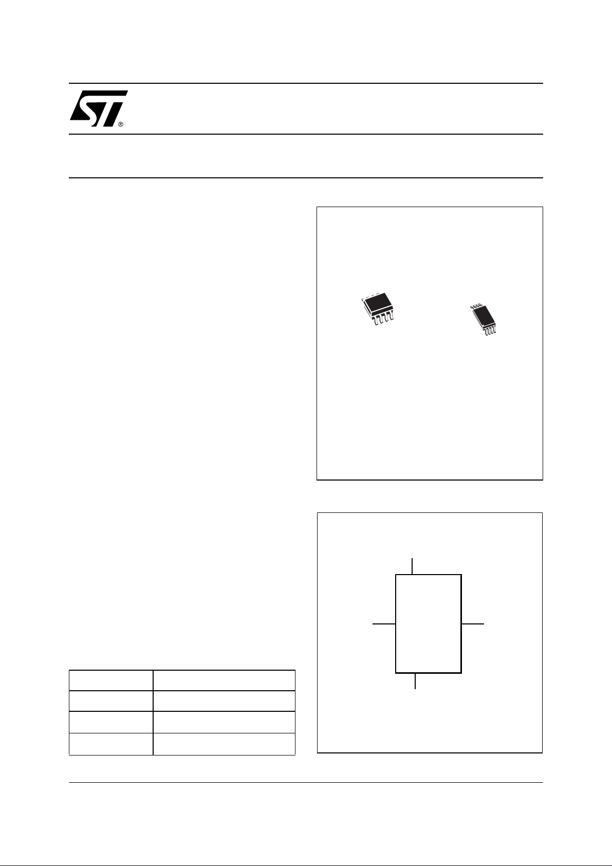
1
SO8 (MN)
150 mil width
Figure 1. Logic Diagram
V
CC
SCL
M34C00
TSSOP8 (DW)
169 mil width
SDA
Table 1. Signal Names
SDA Serial Data
SCL Serial Clock
V
CC
V
SS
August 2001
This is preliminary information on a new product now in development or undergoing evaluation. Details are subject to change without notice.
Supply Voltage
Ground
V
SS
AI03394
1/15
Page 2
M34C00
Figure 2A. SO and TSSOP Connections
When data is read by the bus master, the bus
master acknowledges the receipt of t he data b yte
in the same way. Data transfers are terminated by
a Stop condition after an Ack for Write, and after a
M34C00
NC V
1
2
NC
SS
3
4
8
7
6
5
AI03395B
CC
NCNC
SCL
SDAV
NoAck for Read.
Power On Reset: V
Lock-Out Write Protect
CC
In order to prevent data corruption and inadvertent
Write operations during Power-up, a Power On
Reset (POR) circuit is included. The internal reset
is held active until V
has reached the POR
CC
threshold value, and all operations are disabled –
the device will not respond to any command. In the
same way, when V
drops from the operating
CC
voltage, below the POR threshold value, all
operations are disabled and the device will not
Note: 1. NC = Not Connected
respond to any com ma nd. A s table a nd v alid V
CC
must be applied before applying any logic signal.
2
These devices are compatible with the I
memory standard. This is a two wire serial
interface that uses a bi-directional data bus and
serial clock. The device carries a built-in 4-bit
Device Type Identifier code (1010) in accordance
with the I
2
C bus definition to access the memory
area and a second Device Type Identifier code
(0110) to access the Protection Register.
2
The device behaves as a slave in the I
C protocol,
with all memory operations synchronized by the
serial clock. Read and Write operations are
initiated by a Start condition, generated by the bus
master. The Start condition is followed by a Device
Select code and RW
bit (as described in Table 3),
terminated by an acknowledge bit.
When writing data to the memory, the device
inserts an acknowledge bit during the 9
th
bit time,
following the bus master’s 8-bit transmission.
C
SIGNAL DESCRIPTION
Serial Clock (SCL)
This signal is used to strobe all data in and out of
the device. In appli cations where this line is used
by slave devices to synchronize the bus to a
slower clock, the bus master must have an open
drain output, and a pull-up resistor must be
connected from Serial Clock (SCL) to V
3 indicates how t he value of the pull-up resistor
can be calculated). In most applications, t hough,
this method of synchronization is not employed,
and so the pull-up resistor is not necessary,
provided that the bus master has a push-pull
(rather than open drain) output.
Serial Data (SDA)
This bi-directional signal is used to transfer data in
or out of the device. It is an open drain output that
. (Figure
CC
may be wire-OR’ed with other open drain or open
Table 2. Absolute Maximum Ratings
Symbol Parameter Value Unit
T
A
T
STG
T
LEAD
V
IO
V
CC
V
ESD
Note: 1. Except for the rating “Operating Temperature Ra nge”, stresses above those li sted in t he Table “Absolute M aximum Ratings” may
cause permanent damage to the device. These are stress ratings only, and operation of the device at these or any other conditions
above those indi cated in t he Operating sect i ons of thi s specifi cation i s not impl i ed. Exposure to Absolute M aximum Rating c onditions for extended periods may affect device reliability. Refer also to the ST SURE Program and other relevant quality documents.
2. IPC/JEDEC J- S T D- 020A
3. JEDEC Std JESD22-A 114A (C1=1 00 pF, R1=1500 Ω, R2=500 Ω)
Ambient Operating Temperature –40 to 85 °C
Storage Temperature –65 to 150 °C
Lead Temperature during Soldering
Input or Output range –0.6 to 6.5 V
Supply Voltage –0.3 to 6.5 V
Electrostatic Discharge Voltage (Human Body model)
1
SOT23: t.b.d.
SO: 20 seconds (max)
TSSOP: 20 seconds (max)
2
3
2
t.b.d.
235
235
4000 V
°C
2/15
Page 3
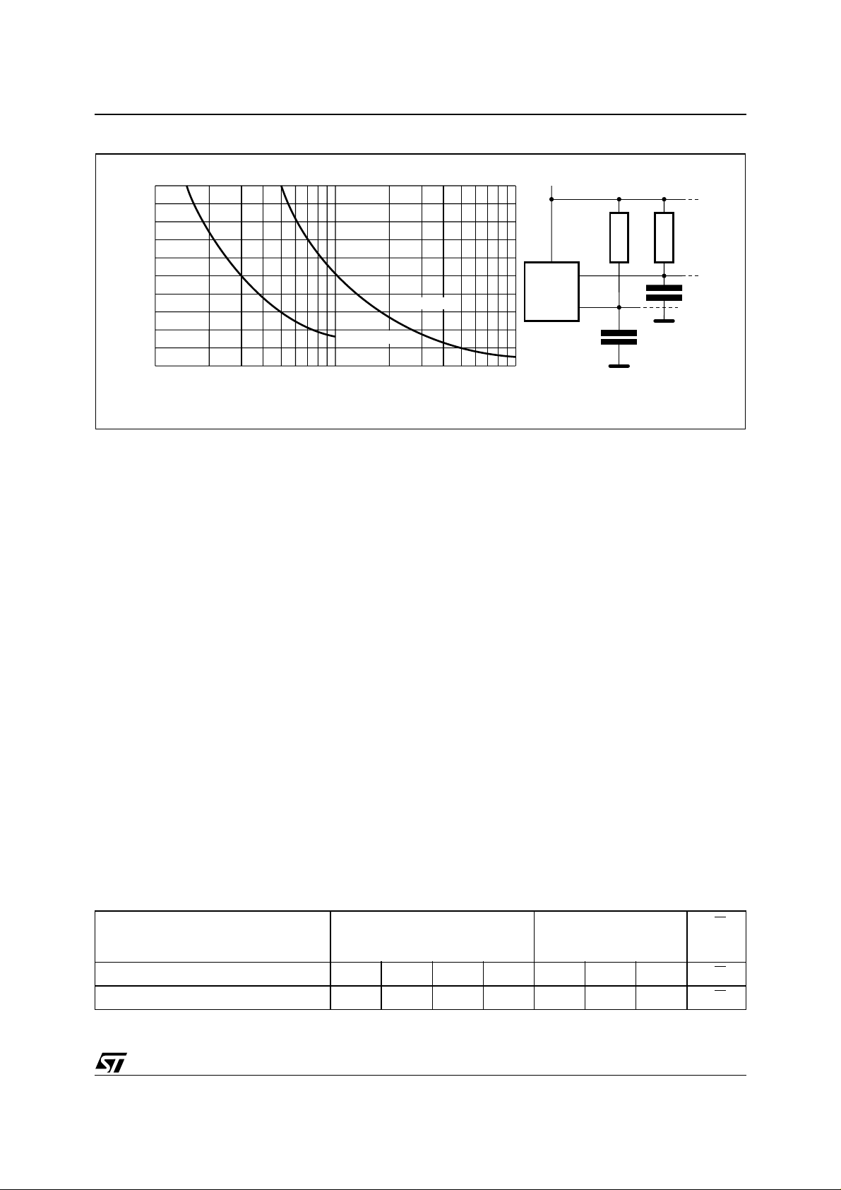
M34C00
Figure 3. Maximum RL Value versus Bus Capacitance (C
20
16
12
8
Maximum RP value (kΩ)
4
0
10 1000
C
BUS
fc = 400kHz
100
(pF)
collector signals on the bus. A pull up resistor must
be connected from Serial Data (SDA) to V
(Figure 3 indicates how the value of the pull-up
resistor can be calculated).
fc = 100kHz
.
CC
Stop Condition
Stop is identified by a rising edg e of Serial Data
(SDA) while Serial Clock (SCL) is stable, and
driven High. A Stop condition terminates
communication between the device and the bus
DEVICE OPERATION
The device supports the I
2
C protocol. This is
summarized in Figure 4. Any device that sends
data on to the bus is defined to be a transmitte r,
and any device that reads the data to be a
receiver. The device that controls the data transfer
is known as the bus master, and the other as the
slave device. A data transfer can only be initiated
by the bus master, which will also provide the
serial clock for synchronization. The M34C00
device is always a slave in all communication.
Start Condition
Start is identified by a falling edge of Serial Data
(SDA) while Serial Clock (SCL) is stable in the
High state. A Start condition must precede any
data transfer command. The devi ce continuously
monitors (except during a programming cycle)
Serial Data (SDA) and Serial Clock (SCL) for a
Start condition, and will not re sp ond unless one is
master. A Read command that is followed by
NoAck can be followed by a Stop condition to force
the device into the Stand-by mode. A Stop
condition at the end of a Write command triggers
the internal EEPRO M Writ e cycle.
Acknowledge Bit (ACK)
The acknowledge bit is used to indicate a
successful byte transfer. The bus transmitter,
whether it be bus master or slave device, releases
Serial Data (SDA) after sending eight bits of data.
During the 9
Serial Data (SDA) Low to acknowledge the receipt
of the eight data bits.
Data Input
During data input, the device samples Serial Data
(SDA) on the rising edge of Serial Clock (SCL).
For correct device operation, Serial Data (SDA)
must be stable during the rising edge of Serial
Clock (SCL), and the data on Serial Data (SDA)
given.
) for an I2C Bus
BUS
MASTER
th
clock pulse period, the receiver pulls
V
CC
R
SDA
SCL
R
C
BUS
L
C
BUS
AI01665
L
Table 3. Device Select Code
Device Type Identifier
b7 b6 b5 b4 b3 b2 b1 b0
Memory Area Select Code (three arrays) 1 0 10111RW
Protection Register Select Code 0 1 10111RW
Note: 1. The most signi ficant bit (b7) is sent fir st .
1
RW
3/15
Page 4
M34C00
Figure 4. I2C Bus Protocol
SCL
SDA
SCL
SDA
SCL
SDA
START
Condition
START
Condition
1 23 789
MSB
1 23 789
MSB ACK
SDA
Input
SDA
Change
STOP
Condition
ACK
STOP
Condition
AI00792B
must change
only
when Serial Clock (SCL) is
driven Low.
Memory Addressing
To start communication betwee n the bus master
and the slave device, the bus mas ter mus t initiate
a Start condition. Following this, t he bus master
sends the 8-bit byte, shown in Table 3, on Serial
Data (SDA) (most significant bit first). This
consists of the 7-bit Device Select code, and the
Read/Write
bit (RW).
To address the memory array, the 4-bit Device
Type Identifier is 1010b. To address the Protection
Register, it is 0110b, as shown in Table 3.
th
The 8
bit is the Read/Write bit (RW). This bit is
set to 1 for Read and 0 for Write operations. If a
match occurs on the Device Select code, the
corresponding device gives an acknowledgment
on Serial Data (SDA) during the 9
th
bit time. If the
device does not match the Device Select code, it
4/15
deselects itself from the bus, and goes into Standby mode.
Memory Partition in g
The memory is divided in three arrays:
■ Array-0: Write-protectable Array (00h to 0Fh)
■ Array-1: EEPROM Array (10h to 1Fh)
■ Array-2: Non-Erasable Memory Array (20h to
2Fh)
The 4 least significant bits of the address byte
determine the byte that is to be addressed within
the given array. The next 2 more significant
address bits determine the array that is to be
addressed (Array-0, Array-1, Array-2 or Invalid).
The 2 most significant address bits are Don’t Care.
If the address is of the form xx11xxxx, the device
recognises that an attempt is being made to
Page 5
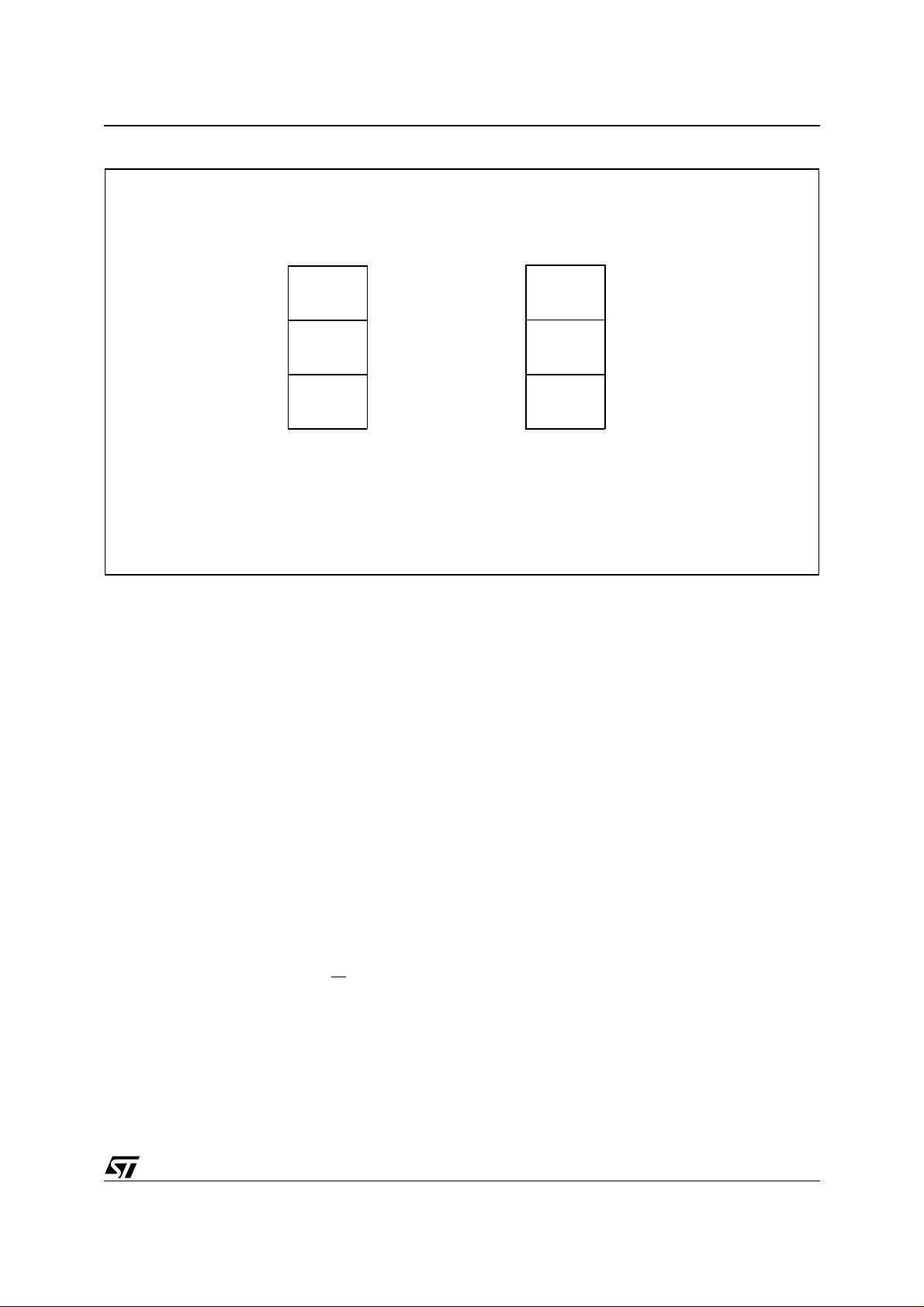
Figure 5. Me m ory P a rti tioning
M34C00
Array 2
Array 1
Array 0
Default EEPROM memory area
state before write access
to the Protection Register
EPROM
Array
Standard
Array
Standard
Array
2Fh
20h
1Fh
10h
0Fh
00h
address the Invalid array, and immediately
deselects itself.
The Write-protectable array consists of 16 bytes of
EEPROM, which can be used as normal EEPROM
until this array is set in its Write-protected mode.
Once Write-protected, this array becomes
functionally equivalent to a Read-Only Memory
(ROM), and cannot be modified further. The
procedure to set this array in its Write-protected
mode is described later.
Array-2 also consists of 16 bytes of EEPROM, but
configured to give the functional equivalence of
non-erasable memory. That is, it is initialized to
contain all 1s (FFh), with the user able to reset any
1 to a 0, but unable to set any 0 to a 1. One
application envisaged for this array is as a nonresettable 128-token array.
WRITE AND READ OPERATIONS
Write Operations
Following a Start condition the bus master sends
a Device Select code with the R W
bit reset to 0.
The device acknowledges this, as shown in Figure
6, and waits for an address byte. The device
responds to the address byte with an acknowledge
bit, and then waits for the data byte.
Byte Write
After the Device Select code and the address byte,
the bus master sends one data byte. If the
addressed location is in the Write-protected area,
Array 2
Array 1
Array 0
EPROM
Array
Standard
Array
Write
Protected
Array
State of the EEPROM memory
area after write access
to the Protection Register
2Fh
20h
1Fh
10h
0Fh
00h
AI03396
the device replies with NoAck, and the l ocation is
not modified. If, instead, the addressed location is
not in a Write-protected area , t he device replies
with Ack. The bus m aster terminates the tran sfer
by generating a Stop condition, as shown in Figure
6.
During the internal Write cycle, Serial Da ta (SDA)
is disabled internally, and the device does not
respond to any requests.
Minimizing System Delays by Polling On ACK
During the internal Write cycle, the device
disconnects itself from the bus, and copies the
data from its internal latches to the memory cells.
The ma x imum Write time (t
) is shown in Table 6,
w
but the typical time is shorter. To make use of this,
an Ack polling sequenc e can be used by t he bus
master.
The sequence, as shown in Figure 7, is:
– Initial condition: a Write cycle is in progress.
– Step 1: the bus master issues a Start con dition
followed by a D evice S ele ct code (the first byte
of the new instruction).
– Step 2: if the device is busy with the internal
Write cycle, no Ack will be returned and the bus
master goes back to Step 1. If the device has
terminated the internal Write cycle, it responds
with an Ack, indicating that the device is ready
to receive the second part of the next instruction
(the first byte of this instruction having been sent
during Step 1).
5/15
Page 6

M34C00
Figure 6. Byte Write Sequences (showing differences in Ackno wledg e bits )
ACK ACK ACK
BYTE WRITE
in Array-1 and Array-2
(and in Array-0, if unprotected)
BYTE WRITE
in Array-0, if protected
DEV SEL BYTE ADDR DATA IN
R/W
START
DEV SEL BYTE ADDR DATA IN
R/W
START
Figure 7. Wri te Cy cle Pol l in g Fl owchart usin g A C K
WRITE Cycle in Progress
(to be followed by a READ)
START Condition
STOP
ACK NO ACK NO ACK
STOP
AI03715B
WRITE Cycle in Progress
(to be followed by a WRITE)
START Condition
NoACK
STOP
DEVICE SELECT
with RW = 1
No
No
ACK
Returned
Yes
Read Data Byte
Continue
the Sequential
Read
ACK
Yes
ReSTART
STOP
DEVICE SELECT
with RW = 0
No
No
ACK
Returned
Yes
Next
Operation is a
Write
Yes
Send Address Byte
ACK
Send Data Byte
ACK
STOP
AI03716B
6/15
Page 7

M34C00
Read Operation
Following a Start condition, t he bus master sends
a Device Select code with the RW
bit set to 1. The
device acknowledges this, and outputs the byte in
location 00h. The counter is then incremented,
and the device continues to output the next byte in
sequence. To terminate the strea m of bytes, the
bus master must
output, and
not
acknowledge the last byte
must
generate a Stop condition, as
shown in Figure 8.
The output data comes from consecutive
addresses, with the internal address counter
automatically incremen ted af t er ea ch byt e out put.
After the last memory address, the internal
address counter rolls over, to continue reading
from the start of the memory.
Acknowledge in Read Mode
For all Read commands, the device waits, after
each byte read, for an acknowledgment during the
th
9
bit time. If the bus m aster does not pu ll Serial
Data (SDA) Low during this time, the device
terminates the data transfer and switches to its
Stand-by mode.
Setting the Write-Protection by Writing to the
Protection Register
The M34C00 has a software Write-protection
function, using the Protection Register, that allows
the bottom 16 bytes of the memory area
(addresses 00h to 0Fh) to be permanent ly Write-
Table 4. Write Time
Write
1
Time
WRITE to Array-0 (when not protected)
WRITE to Array-0 (when Write-protected) 0
WRITE to Array-1
WRITE to Array-2
Note: 1. For the value to tW please see Table 6.
t
W
t
W
t
W
protected. The Write-protection feature is
activated by writing once to the Protection
Register.
The Protection Register is written with the device
select code set to 0110.1110b (as shown in Figure
9). Address and data bytes m ust be sent with this
command, but their values are all ignored, and are
treated as Don’t Care. Once the Protection
Register has been written, the Wri te-protection of
the first 16 bytes of the memory is enabled, and it
is not possible to unprotect these 16 bytes, even if
the device is powered off and on.
When the Protection Register has been written,
the M34C00 no longer responds to the device type
identifier 0110b for either Read or Write
operations.
Figure 8. Read Sequence
SEQUENTIAL READ
of first N bytes
ACK ACK ACK NO ACK
DEV SEL DATA 0
R/W
START
DATA N-1
STOP
AI03717
7/15
Page 8

M34C00
Figure 9. Setting the Protection Register
If the Protection Register has not yet been set:
Device Select
Code
Start
RW
Byte Address
Data In
Stop
SDA
ACK
If the Protection Register has already been set:
Device Select
Code
Start
SDA
RW
NoACK
Reading the Protection Register
To determine whether the Write-protection feature
has been activated, it is possible to read the
Protection Register, as shown in Figure 10.
– If the Protection Register has not been s et, the
device acknowledges the read sequence
– If the Protection Register has been set, the
device deselects itself after it has received the
device select code. Consequently, each part of
the sequence is not acknowledged.
Don't Care
Byte Address
Don't Care
ACK
NoACK
Don't Care
Data In
Don't Care
ACK
NoACK
Stop
AI03718
Figure 10. Reading the Protection Register
If the Protection Register has not yet been set:
SDA
If the Protection Register has been set:
SDA
8/15
Device Select
Code
Start
Device Select
Code
Start
RW
ACK
RW
NoACK
Data Out
FFh
Data Out
FFh
NoACK
NoACK
Stop
Stop
AI03719B
Page 9

M34C00
Table 5. DC Characteristics (TA = –40 to 85 °C; VCC = 2.5 to 5.5 V )
Symbol Parameter Test Condition Min. Max. Unit
Input Leakage
I
LI
I
LO
I
CC
I
CC1
V
IL
V
IH
V
OL
Current
Output Leakage Current
Supply Current
Supply Current
(Stand-by)
Input Low
Voltage
Input High
Voltage
Output Low
Voltage
SCL, SDA 0 V ≤ V
0V ≤ V
OUT
=5.5V, fc=400kHz (rise/fall time <
V
CC
=2.5V, fc=400kHz (rise/fall time <
V
CC
V
= VSS or V
IN
V
= VSS or V
IN
SCL, SDA –0.3
SCL, SDA
I
= 3 mA, V
OL
I
= 2.1 mA, V
OL
≤ V
30ns)
30ns)
≤ V
IN
CC
SDA in Hi-Z
CC,
, V
CC
CC
= 5.5 V
CC
, V
= 2.5 V 1 µA
CC
0.3V
0.7V
CC
= 5.5 V 0.4 V
CC
= 2.5 V 0.4 V
CC
± 2 µA
± 2 µA
2mA
1mA
2µA
CC
VCC+1
V
V
Table 6. AC Characteristics
M34C00
V
=2.5 to 5.5V
Symbol Alt. Parameter
t
t
CH1CH2
t
CL1CL2
2
t
DH1DH2
2
t
DL1DL2
t
CHCL
t
CLCH
t
CHDX
t
DLCL
t
DXCX
t
CLDX
t
CHDH
t
DHDL
t
CLQV
t
CLQX
f
C
t
W
Note: 1. For a reSta rt condition , or following a Write cycle.
2. S am p l ed only, not 100 % t ested.
3. To avoid spurious Start and Stop conditions, a minimum delay is placed between SCL=1 and the falling or rising edge of SDA.
t
HIGH
t
LOW
1
t
SU:STA
t
HD:STA
t
SU:DAT
t
HD:DAT
t
SU:STO
t
BUF
3
t
t
f
SCL
t
Clock Rise Time 300 ns
R
t
Clock Fall Time 300 ns
F
t
SDA Rise Time 20 300 ns
R
t
SDA Fall Time 20 300 ns
F
Clock Pulse Width High 600 ns
Clock Pulse Width Low 1.3 µs
START Set-up Time 600 ns
START Hold Time 600 ns
SDA In Set-up Time 100 ns
SDA In Hold Time 0 µs
STOP Set-up Time 600 ns
Time the bus must be free between STOP and next START 1.3 µs
Clock Low to SDA Out Valid 200 900 ns
AA
SDA Out Hold Time after Clock Low 200 ns
DH
Clock Frequency 400 kHz
Write Time 10 ms
WR
CC
T
= –40 to 85°C
A
Min Max
Unit
9/15
Page 10

M34C00
Figure 11. AC Measurement Conditions
0.8V
0.2V
CC
CC
Input Rise and Fall Times
Input Pulse Voltages
Input and Output Timing
Reference Voltages
<= 50 ns
0.2V
to 0.8V
CC
0.3VCC to 0.7V
CC
CC
Table 7. Input Parameters 1(TA = 25 °C, f = 400 kHz)
Symbol Parameter Test Condition Min. Max. Unit
0.7V
0.3V
AI03766
CC
CC
C
IN
C
IN
t
NS
Input Capacitance (SDA) 8 pF
Input Capacitance (other pins) 6 pF
Pulse width ignored
(Input Filter on SCL and SDA)
Note: 1. Sampled only, not 100% tested.
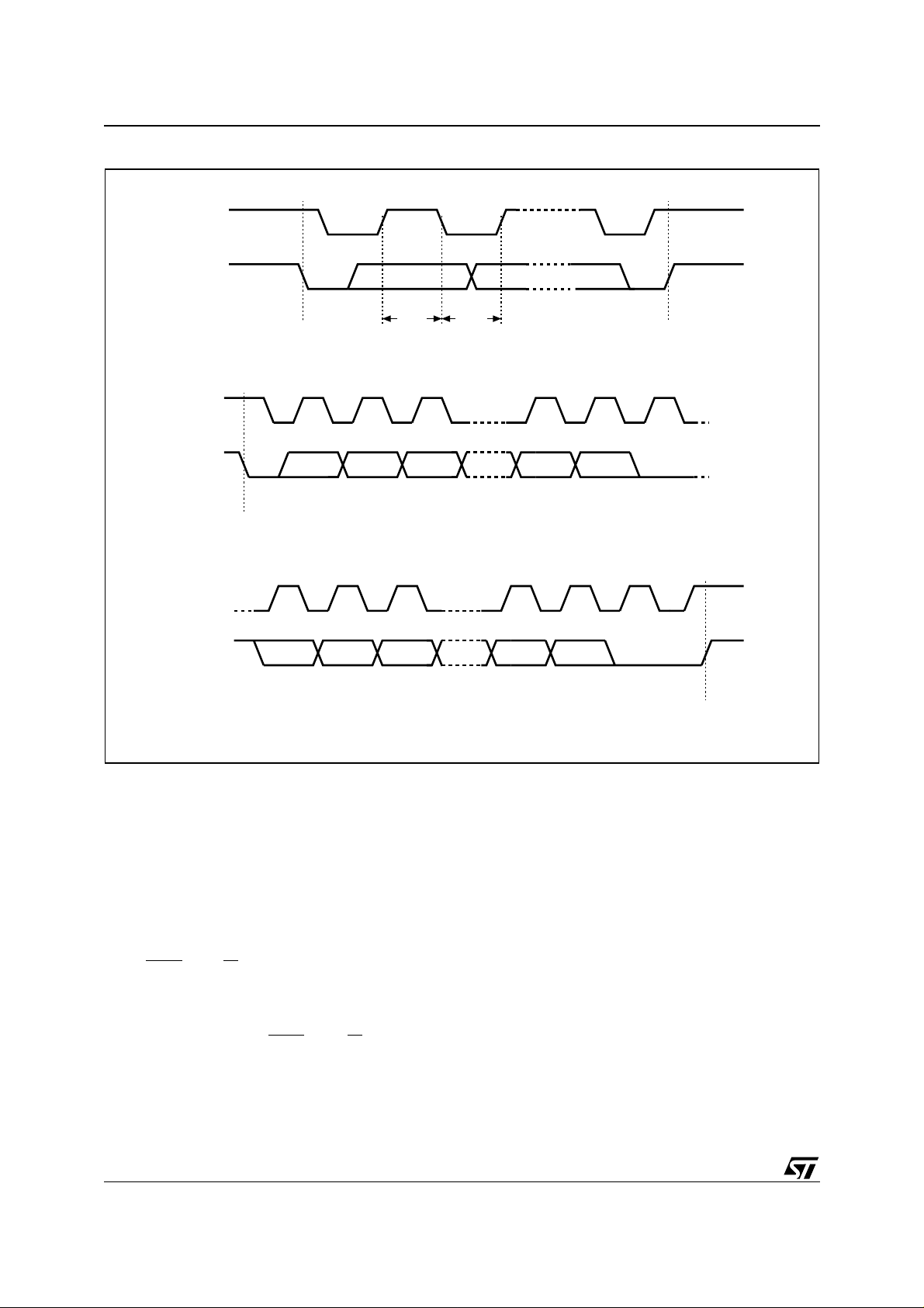
Figure 12. AC Waveforms
tCHCL
SCL
tDLCL
SDA In
tCHDX
START
Condition
SCL
SDA
Input
Single glitch 100 500 ns
tCLCH
tDXCXtCLDX
SDA
Change
tCHDH tDHDL
STOP
Condition
Condition
START
10/15
SDA In
SCL
SDA Out
tCHDH
STOP
Condition
tCLQV tCLQX
Data Valid
tW
Write Cycle
tCHDX
START
Condition
AI00795C
Page 11

M34C00
Table 8. Ordering Information Scheme
Example: M34C00 –W MN 6 T
Operating Voltage Option
W 2.5 V to 5.5 V T Tape and Reel Packing
Package Temperature Range
MN SO8 (150 mil width) 6 –40 °C to 85 °C
DW TSSOP8 (169 mil width)
ORDERING INFORMATION
Devices are shipped from the factory with the
memory content set at all 1s (FFh), and the
Protection Register set at all 0s (00h).
The notation used for the device number is as
shown in Table 8. For a list of avai lable options
(speed, package, etc.) or for further information on
any aspect of this device, please contact your
nearest ST Sales Office.
11/15
Page 12

M34C00
SO8 narrow – 8 lead Plastic Small Outline, 150 mils body width
h x 45˚
A
B
e
D
N
1
SO-a
Note: Drawing is not to scale.
CP
E
H
SO8 narrow – 8 lead Plastic Small Outline, 150 mils body width
Symb.
Typ. Min. Max. Typ. Min. Ma x.
A 1.35 1.75 0.053 0.069
A1 0.10 0.25 0.004 0.010
mm inches
C
LA1 α
12/15
B 0.33 0.51 0.013 0.020
C 0.19 0.25 0.007 0.010
D 4.80 5.00 0.189 0.197
E 3.80 4.00 0.150 0.157
e 1.27 – – 0.050 – –
H 5.80 6.20 0.228 0.244
h 0 .25 0.50 0.010 0.020
L 0 .40 0.90 0.016 0.035
α
0° 8° 0° 8°
N8 8
CP 0.10 0.004
Page 13

TSSOP8 – 8 lead Thin Shrink Small Outline
D
M34C00
8
1
CP
Note: 1 . Drawing is not to scale.
5
4
eb
TSSOP8 – 8 lead Thin Shrink Small Outline
Symbol
Typ. Min. M ax. Typ. Min. Max.
A 1.200 0.0472
A1 0.050 0.150 0.0020 0.0059
mm inches
c
EE1
α
A2A
A1
L
L1
TSSOP8-M
A2 1.000 0.800 1.050 0.0394 0.0315 0.0 413
b 0. 190 0.300 0.0075 0.0118
c 0.090 0.200 0.0035 0.0079
CP 0. 100 0.0039
D 3.000 2.900 3. 100 0.1181 0.1142 0.1220
e 0.650 – – 0.0256 – –
E 6.400 6. 200 6.600 0.2520 0.2441 0.2598
E1 4.400 4.300 4.500 0.1732 0.1693 0.1 772
L 0.600 0.450 0. 750 0.0236 0.0177 0.0295
L1 1 .000 0.0394
α
0° 8° 0° 8°
13/15
Page 14

M34C00
Table 9. Revision History
Date Rev Description of Revision
05-Jan-2000 1.0 Document written
Wording changes, according to the standard glossary
16-Oct-2000 1.1
26-Feb-2001 1.2
08-Jun-2001 1.3
Explanation of Writing to the Protection Register, and Reading from it
Addition of the SOT23-5 package on pp 1, 2, ordering info, and mechanical data
SOT23 Connections modified
Paragraphs added on Don’t Care bits in the address byte, and the effect of address in the
Invalid array
Attempts to read beyond the end of the memory cause roll-over to occur
Reading the protection register does not involve sending an address byte
Lead Soldering Temperature in the Absolute Maximum Ratings table amended
Write Cycle Polling Flow Chart using ACK illustration updated
Package mechanical data updated for TSSOP8 package according to JEDEC\MO-153
27-Aug-2001 1.4
Document promoted from “Product Preview” to “Preliminary Data” status
SOT23-5 package removed
14/15
Page 15

M34C00
Information furnished is believed to be accurate and reliable. However, STMicroelectronics assumes no responsibility for the consequences
of use of such information nor for any infringement of patents or other rights of third parties which may result from its use. No license is granted
by implic ation or otherwise under any patent or p atent rights of STMi croelectr oni cs. Spec i fications mentioned i n this publicatio n are subject
to change without notice. This publication supersedes and replaces all information previously supplied. STMicroelectronics products are not
authorized for use as cri tical comp onents in life support dev i ces or systems wi t hout expres s written approval of STMi croelectr o nics.
The ST logo is registered trademark of STMicroelectronics
All other names are the propert y of their respective owners
© 2001 STMicroelectronics - All Rights Reserved
Australi a - Brazil - Ch i na - Finland - Fr ance - Germa n y - Hong Kong - India - Italy - J apan - Malays ia - Malta - Morocco -
Singap ore - Spain - Sweden - Swit zerland - Uni ted Kingdom - U.S.A.
STMicroelectronics GROUP OF COMPANIES
www.st.com
15/15
 Loading...