

CMOS 12 X 8 CROSSPOINT WITH CONTROL MEMORY
.LOW ON RESISTANCE
(typ.60Ω at V
DD
=10V)
.INTERNAL CONTROL LATCHES
.ANALOGSIGNALSWINGCAPABILITYEQUAL
TOPOWER SUPPLYVOLTAGEAPPLIED
.LESSTHAN1 % TOTALDISTORT. AT 0 dBm
.
LESSTHAN – 95 dB CROSS-TALK
AT1 KHz 1 V
.
VERYLOW POWERCONSUMPTION
PP
.PIN-TO-PINCOMPATIBLEWITHM093
DESCRIP TION
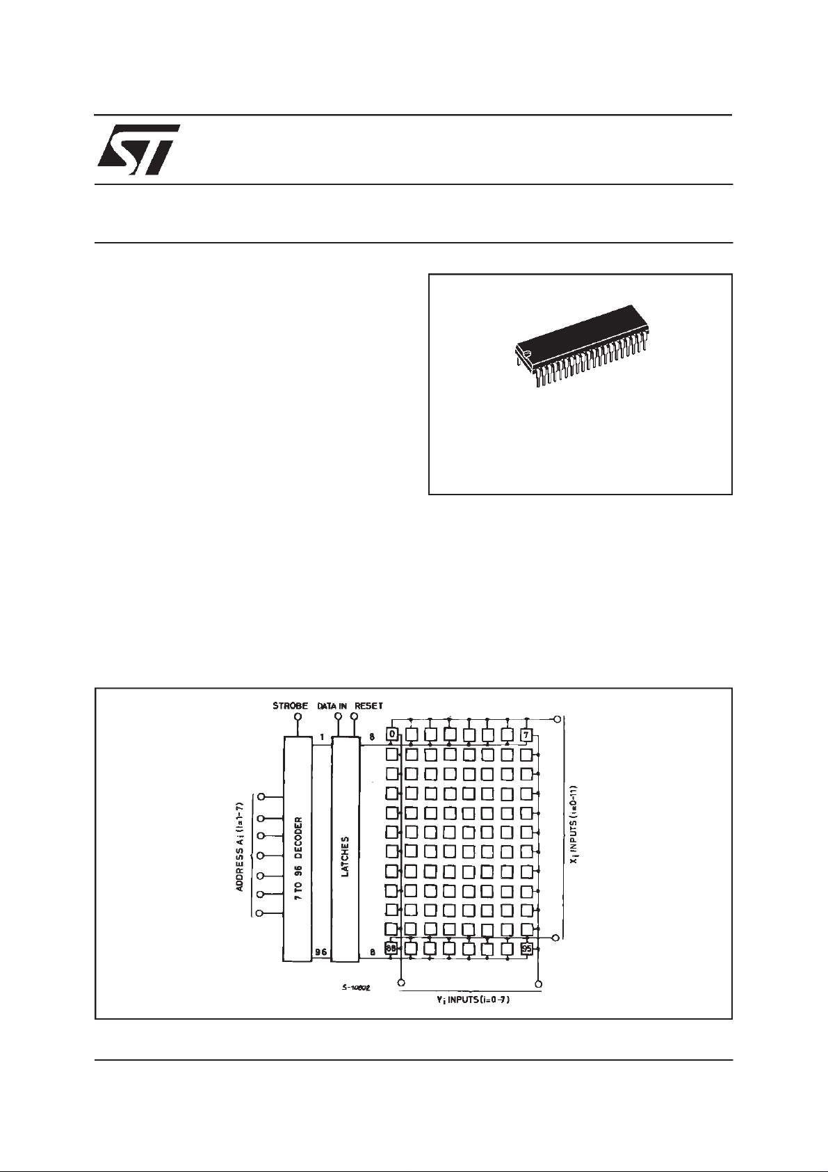
TheM3493containsa12 x 8 arrayof crosspointtogetherwitha 7 to96linedecoderandlatchcircuits.
Anyoneof the96 switchescanbe addressedby selecting the appropriate 7 input bits. The selected
switch can be turnedon or off by applying a logical
oneorzerotothedatain andthestrobeinputat logi-
M3493B2
DIP40
ORDERING NUMBER : M3493B2 (*)
(*) It substitutesthe obsolete M3493B1.
calone.A resetsignalcanbeused to turnoff allthe
switchestogetherwhenis switchedat logicalone.
M3493 is available in 40 lead dual in-line plastic
package.
BLOCKDIAGRAM
June 1998
1/12
M3493B2
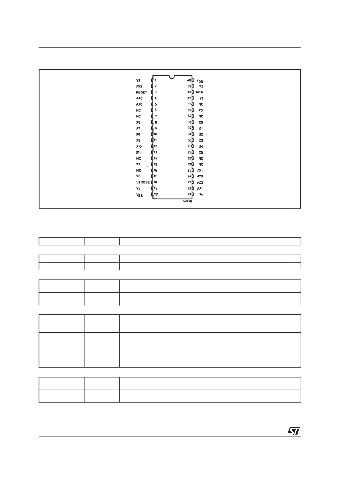
PIN CONNECTION
(top v iew)
INPUT/OUTPUT DESCRIPTION
I/O Symbol Pin Description
POWER
IV
IV
ADDRESS
I AX0-AX3 4, 5, 22, 23 X Address Lines. These 4 pins are used to select one of the 12 rows of
I AY0-AY2 2, 24, 25 Y Address Lines. These 3 pins are used to select one of the 8 columns of
CONTROL
I DATA 38 This input determines if the selected switch will be turned on (closed) or off
I STROBE 18 This pin enables whatever action is selected by the ADDRESS and DATA pins.
I RESET 3 Master Reset. This pin turns off (opens) all 96 switches. The states of the
DATA
I/O X0-X11 8-13, 28-33 Analog Input/Outputs. These pins are connected to the Y0-Y7 pins in according
I/O Y0-Y7 1,15,17,19,21
DD
SS
40 Positive Power Supply
20 Negative Power Supply
switches. Refer to the truth table for legal address.
switches. Refer to the truth table for legal address.
(opened). If the pin is held high, the selected switch will be closed.
If the pin is held low, the switch will be opened.
When the STROBE pin is held low, no switch openings or closings take place.
When the STROBE pin is held high, the switch addressed by the select lines
will be opened or closed (depending upon the state of the DATA pin)
above control lines are irreleant. This pin is active high.
to the truth table.
35,37,39
Analog Input/Outputs. These pins are connected to the X0-X15 pins in
according to thetruth table.
2/12
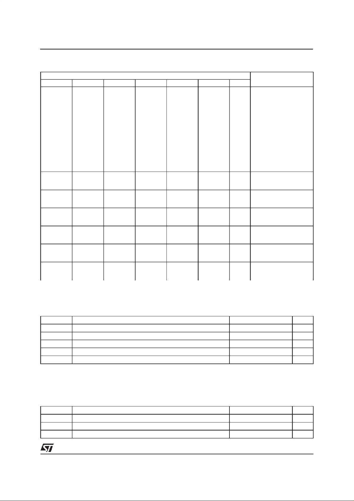
TRUTH TABLE
Address Connections
AX0 AX1 AX2 AX3 AY0 AY1 AY2
0
1
0
1
0
1
0*
1*
0
1
0
1
0
1
0*
1*
0
↓
1
0
↓
1
0
↓
1
0
↓
1
0
↓
1
0
↓
1
0
0
1
1
0
0
1
1
0
0
1
1
0
0
1
1
0
↓
0
0
↓
0
0
↓
0
0
↓
0
0
↓
0
0
↓
0
0
0
0
0
1
1
1
1
0
0
0
0
1
1
1
1
0
↓
1
0
↓
1
0
↓
1
0
↓
1
0
↓
1
0
↓
1
0
0
0
0
0
0
0
0
1
1
1
1
1
1
1
1
0
↓
1
0
↓
1
0
↓
1
0
↓
1
0
↓
1
0
↓
1
0
0
0
0
0
0
0
0
0
0
0
0
0
0
0
0
1
↓
1
0
↓
0
1
↓
1
0
↓
0
1
↓
1
0
↓
0
0
0
0
0
0
0
0
0
0
0
0
0
0
0
0
0
0
↓
0
1
↓
1
1
↓
1
0
↓
0
0
↓
0
1
↓
1
M3493B2
0
0
0
0
0
0
0
0
0
0
0
0
0
0
0
0
0
↓
0
0
↓
0
0
↓
0
1
↓
1
1
↓
1
1
↓
1
X0 - Y0
X1 - Y0
X2 - Y0
X3 - Y0
X4 - Y0
X5 - Y0
No connection
No connection
X6 - Y0
X7 - Y0
X8 - Y0
X9 - Y0
X10 - Y0
X11 - Y0
No connection
No connection
X0 - Y1
<0>
↓
↓
X11 - Y1
X0 - Y2
↓↓
X11 - Y2
X0 - Y3
↓↓
X11 - Y3
X0 - Y4
↓↓
X11 - Y4
X0 - Y5
↓↓
X11 - Y5
X0 - Y6
↓↓
X11 - Y6
ABSOLUTE MAXIMUM RATINGS
Symbol Parameter Value Unit
V
DD
V
IN
P
tot
T
oper
T
stg
Str e s ses above those list ed under ”Absolu te Ma ximum R at i ngs” may c a us e permanent damage to the device. T hi s is a stress
rat ing only and funct ional operation of t he devi ce at these or any other conditions in excess of t hose in di c ated i n the opera t i onal
sect i ons of thi s specificat i on is not im plied. Ex posur e to absolute m aximum rating conditions for ex t ended per iods m ay affect
devi ce reliabili t y.
DC supply Voltage - 0.5, 14 V
Input Voltage Range - 0.5, VDD+ 0.5 V
Power Dissipation 1 W
Operating Temperature Range 0, + 70
Storage Temperature Range - 50, + 125
o
o
C
C
RECOMMENDED OPERATING CONDITIONS
Symbol Parameter Value Unit
V
DD
T
oper
V
IN
Supply Voltage 10 V
Operating Temperature 0, + 70
(Logic Signal) 0, V
DD
o
V
C
3/12
M3493B2
STATIC ELECTRICAL CHARACTERISTICS (T
= 0 to 70oC, VDD= 10V, unless otherwise specified
amb
Symbol Parameter Test Conditions Min. Typ. Max. Unit
I
Supply Current Reset = V
S
DD
1mA
CROSSPOINT
On Resistance V
= 4.75V, V
IDC
= 4.5V, See Figure 1 60 100
ODC
On Resistance Variation 10 20 Ω
Off-leakage * All switches off V
OS=VIS
= 0 toV
DD
± 3 µA
CONTROLS
V
IL
V
IH
Input Leakage * V
* The device is guaranteed with such limits up to 70°C. At 25°C these limits become±100nA.
= 0 to V
IN
DD
2.4 V
0.8 V
3
±
DYNAMIC ELECTRICAL CHARACTERISTICS
=25oC, CL= 50pF all input square wave rise and fall times = 10ns, VDD= 10V)
(T
amb
Symbol Parameter Test Conditions Min. Typ. Max. Unit Fig.
CROSSPOINT
,
t
t
Propagation Delay Time (switch on)
PHL
Signal Input to Output
PLH
Frequency Response (any switch on)
20 log (V
OS/VIS
) = -3dB
Sine Wave Distortion
Feed Through (any switches off)
Frequency for Signal Crosstalk
Attenuation of 40dB
Attenuation of 110dB
C Capacitance
Xn to Ground
Vn to Ground
Feed Through
C Capacitance Logic Input to Ground f
CONTROLS (t
t
PSN
t
PZH
t
PAN
t
PSF
t
PZL
t
PAF
t
S
t
H
t
O
t
W
t
WR
t
PHZ
t
AS
t
AH
= 10ns)
r,tf
Propagation Delay Time Strobeto
Output (switch turn-on to high level)
Data-in to Output (turn-on to high level) 150 200 ns 6
Address to Output (turn-on to high level) 150 200 ns 7
Propagation Delay Time Strobeto
Output (switch turn-off)
Data-in to Output (turn-on to low level) 150 200 ns 6
Address to Output (turn-off) 150 200 ns 7
Set-up Time Data-in to Strobe 40 ns 5
Hold Time Data-in to Strobe 120 ns 5
Switching Frequency 1 MHz
Strobe Pulse Width 100 ns 10
Reset Pulse Width 150 ns 9
Reset Turn-off to OutputDelay 150 200 ns 9
Address Set-up Time Address to Strobe 120 ns 10
Address Hold Time Address to Strobe 120 ns 10
Control Crosstalk Data-in, Address or
Strobe to Output
=1kΩ,VIS=2V
R
H
R
=81Ω,VIS=2VPP,CL= 3pF
H
= 1kHz, RH= 0.6kΩ,VIS=8V
f
q
= 10kHz, RH=1kΩ,VIS=2V
f
q
=1kΩ,VIS=2V
R
H
= 1MHz, VIS= 0.1V
f
q
= 1MHz, VIS= 0.1V
q
=1kΩ,CL= 50pF
R
L
Square wave input, V
R
= 10k
Ω
L
PP
PP
PP
PP
IN
= 3V,
PP
PP
30 100 ns 2
50 MHz
1%
-80 dB 3
1
5
MHz
kHz
pF
15
15
0.4
5pF
150 200 ns 5
150 200 ns 5
75 mV 8
Ω
A
µ
4
10
10
4/12

TEST CI R CUITS
M3493B2
Figure 1 : R
Measurement. Figure2 : PropagationDelayTime and Wave-
ON
Figure 3 : Off IsolationMeasurement(Feedthrough).
forms(signalinput to signaloutput
switchON).
5/12

M3493B2
Figure 4 : CrosstalkMeasurements.
Figure 5 : PropagationDelay Time and Waveforms (strobeto signaloutput switchTurn-ONor Turn-OFF).
Figure 6 : PropagationDelay Time and Waveforms (data-insignal output,switchTurn-ONtohigh or
lowlevel).
6/12

Figure 7 : PropagationDelay Time and Waveforms (addressto signaloutputswitch Turn-ONor
Turn-OFF).
M3493B2
Figure 8 : Waveformsfor Crosstalk(controlinput to signaloutput).
7/12

M3493B2
Figure 9 : PropagationDelay Time and Waveforms (resetto outputdelay).
Figure 10 : PropagationDelayTime andWaveforms(Strobeand C/S to signal outputswitch).
8/12

Figure 11 : TypicalRONversusVis.
Figure 12 : Peakto Peak VoltageCapabilityversusTotal HarmonicDistortion.
M3493B2
Figure 13 : V
CapabilityversusVDD.
RMS
9/12

M3493B2
TYPICAL APP LICATIONS
Thefigures14, 15 and 16 show the systemconfigurationfor expandedmatrices(16 x 16,8 x 64, 32 x 32).
Figure 14 : (16 x 16 nonblocking matrix).
Figure 15 : (8 x 64 matrix).
Figure 16 : (32 x 32 nonblocking matrix).
10/12

DIP40PACKAGEMECHANICAL DATA
M3493B2
DIM.
MIN TYP MAX MIN TYP MAX
a1 0.63 0.025
b 0.45 0.018
b1 0.23 0.31 0.009 0.012
b2 1.27 0.050
D 52.58 2.070
E 15.2 16.68 0.598 0.657
e 2.54 0.100
e3 48.26 1.900
F 14.1 0.555
I 4.445 0.175
L 3.3 0.130
mm inch
11/12

M3493B2
Information furnished is believed to be accurate and reliable. However, STMicroelectronics assumes no responsibility for the consequences of use of such information nor for any infringement of patents or other rights of third parties which may result from its use. No
license is granted by implication or otherwise under any patent or patent rights of STMicroelectronics. Specification mentioned in this
publication are subject to change without notice. This publication supersedes and replaces all information previously supplied. STMicroelectronics products are not authorized for use as critical components in life support devices or systems without express written
approval of STMicroelectronics.
The ST logo is a registeredtrademark of STMicroelectronics
1998 STMicroelectronics – Printed in Italy – All Rights Reserved
Australia - Brazil - Canada - China - France - Germany - Italy - Japan - Korea - Malaysia - Malta - Mexico - Morocco - The Netherlands -
Singapore - Spain - Sweden - Switzerland - Taiwan - Thailand - United Kingdom - U.S.A.
‘STMicroelectronics GROUP OF COMPANIES
12/12
 Loading...