

Page 1
.
FLASHEDOR MODULATED TRANSMISSION
.
7 SUB-SYSTEMADDRESSES
.
UP TO 64 COMMANDS PER SUB-SYSTEM
ADDRESS
.
HIGH-CURRENT REMOTE OUTPUT AT
=6V(–IOH= 80mA)
V
DD
.
LOW NUMBER OF ADDITIONAL COMPONENTS
.
KEY RELEASE DETECTION BY TOGGLE
BITS
.
VERYLOWSTAND-BYCURRENT (< 2µA)
.
OPERATIONAL CURRENT < 1mA AT 6V
SUPPLY
.
SUPPLYVOLTAGE RANGE 2 TO6.5V
.
CERAMIC RESONATOR CONTROLLED
FREQUENCY(typ. 450kHz)
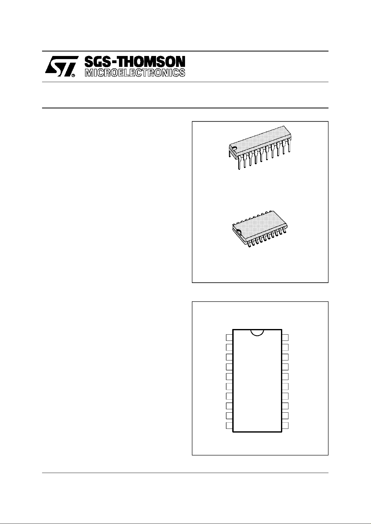
M3004LAB1
M3004LD
REMOTECONTROLTRANSMITTER
DIP20
(Plastic Package)
ORDER CODE : M3004LAB1
DESCRIPTION
The M3004LAB1/M3004LDtransmitter IC are designed for infrared remote control systems. It has
a total of 448 commandswhich are divided into 7
sub-systemgroups with 64 commands each. The
sub-systemcodemay be selectedby a press button, a slider switch or hardwired.
The M3004LAB1/M3004LD generate the pattern
for driving the output stage. These patterns are
pulse distance coded. The pulses are infrared
flashes or modulated. The transmission mode is
defined in conjunction with the sub-system address. Modulated pulses allow receivers with narrow-band preamplifiers for improved noise
rejection to be used. Flashed pulses require a
wide-bandpreamplifierwithin the receiver.
(Plastic Package)
ORDER CODE : M3004LD
PIN CONNECTIONS
SS
1
2
3
4
5
6
7
8
9
10
REMO
SEN6N
SEN5N
SEN4N
SEN3N
SEN2N
SEN1N
SEN0N
ADRM
V
SO20
20
19
18
17
16
15
14
13
12
11
V
DD
DRV 6N
DRV 6N
DRV 6N
DRV 6N
DRV 6N
DRV 6N
DRV 6N
OSC OUT
OSC IN
3004L-01.EPS
June 1992
1/10
Page 2
M3004LAB1 - M3004LD
BLOCK DIAGRAM
0N
1N
S
E
2N
N
I
3N
N
P
4N
U
T
5N
S
6N
V
DD
V
SS
DRVOUTPUTS
0N 1N 3N 4N 5N 6N2N
KEYBOARD
ADRM
OSCILLATOR
OSCI OSCO
SCAN
PULSE
DISTANCE
MODULATOR
CONTROL
LOGIC
REMO
OUTPUT
3004L-02.EPS
INPUTSANDOUTPUTS
Key matrix inputs and outputs (DRV0N to
DRV6Nand SEN0N to SEN6N)
Thetransmitterkeyboardis arrangedas ascanned
matrix.The matrix consists of 7 driveroutputs and
7 sense inputs as shown in Figure 1. The driver
outputs DRV0Nto DRV6Nare opendrainN-channel tran-sistors and they are conductive in the
stand-by mode. The 7 sense inputs (SEN0N to
SEN6N) enable the generation of 56 command
codes.With 2externaldiodesall64commandsare
addressable. The sense inputs have P-channel
pull-uptransistors so that they are HIGH until they
are pulled LOW by connectingthem to an output
viaa keydepressiontoinitiatea codetransmission.
ADDRESS MODEINPUT (ADRM)
The sub-system address and the transmission
mode are defined by connecting the ADRM input
to one or more driveroutputs (DRV0Nto DRV6N)
of the key matrix. If more than one driver is connected to ADRM, they must be decoupled by diodes. This allows the definition of seven
sub-systemaddressesasshownintable3.If driver
DRV6N is connected to ADRM, the data output
format of REMO is modulated or if not connected,
flashed.
The ADRM input has switched pull-up and pulldown loads. In the stand-by mode only the pulldown device is active. Whether ADRM is open
(sub-system address 0, flashed mode) or connected to the driver outputs,this input is LOW and
will not cause unwanted dissipation. When the
transmitterbecomesactive by pressing a key, the
pull-down device is switched off and the pull-up
device is switched on, so that the applied driver
signalsaresensedfor thedecodingof the sub-system addressand the mode of transmission.
The arrangement of the sub-systemaddress coding is such that only the driver DRVnM with the
highest number (n) defines the sub-system address,e.g. if driversDRV2N and DRV4Nare connected to ADRM, only DRV4N will define the
sub-system address. This option can be used in
systems requiring more than one sub-system address. The transmitter may be hard-wired for subsystemaddress2by connectingDRV1Nto ADRM.
If now DRV3N is added to ADRM by a key or a
switch, t h e tran smitte d sub-system a d dress
changesto 4. Achangeof the sub-systemaddress
will not starta transmission.
2/10
Page 3

M3004LAB1 - M3004LD
REMOTECONTROLSIGNAL OUTPUT (REMO)
The REMO signaloutput stage is a push-pulltype.
In the HIGHstate, a bipolaremitter-followerallows
a highoutput current.Thetimingofthedataoutput
formatis listedin tables1 and2.The informationis
defined by the distance t
between the leading
b
edgesof the flashedpulsesor the first edgeof the
modulatedpulses (see Figure3). Theformatof the
output data is given in Figures 2 and 3. The data
wordstarts withtwotoggle bitsT1 andT0,followed
by three bits for defining the sub-system address
S2,S1andS0,andsixbitsF,E,D,C,BandAwhich
are defined by the selected key.
Inthemodulatedtransmissionmodethe firsttoggle
bit is replaced by a constant reference time bit
(REF).Thiscanbe usedasareferencetimefor the
decodingsequence. The toggle bits function is an
indicationfor the decoder that the next instruction
has to be considered as a new command. The
codesfor thesub-systemaddress andtheselected
key are given in tables3 and 4.
The REMO output is protectedagainst ”Lock-up”,
i.e.thelengthof anoutputpulseislimitedto<1ms,
even if the oscillatorstops during an outputpulse.
This avoids the rapid discharge of the battery that
would otherwise be caused by the continuousactivationof the LED.
OSCILLATORINPUT / OUTPUT
(OSCIand OSCO)
The external components must be connected to
these pins when usingan oscillatorwith a ceramic
resonator. The oscillator frequency may vary between350kHzand600kHzasdefinedbythe resonator.
FUNCTIONAL DESCRIPTION
Keyboardoperation
In the stand-by mode all drivers (DRV0N to
DRV6N)areon (lowimpedancetoV
). Whenever
SS
a key is pressed, one or more of the sense inputs
(SENnN) are tied to ground. This will start the
power-upsequence. Firsttheoscillatorisactivated
and afterthe debouncetime t
(see Figure 4) the
DB
output drivers (DRV0N to DRV6N) become active
successively.
Within the first scan cycle the transmissionmode,
the applied sub-system address and the selected
command code are sensed and loaded into an
internal data latch.
In contrast to the commandcode, the sub-system
is sensed only within the first scan cycle. If the
applied sub-system address is changed while the
commandkey is pressed,the transmittedsub-system addressis not altered.
In a multiple key stroke sequence (see Figure 5)
the commandcodeisalways alteredinaccordance
with the sensed key.
MULTIPLEKEY-STROKEPROTECTION
The keyboard is protected against multiple keystrokes. If more than one key is pressed at the
sametime,thecircuitwillnotgenerateanewoutput
at REMO (see Figure 5). In case of a multiple
key-stroke,the scan repetition rate is increasedto
detect the release of a key as soon as possible.
There are two restrictions caused by the special
structureof the keyboard matrix :
- The keys switching to ground(code numbers 7,
15, 23, 31, 39, 47, 55 and 63) and the keys
connectedtoSEN5NandSEN6Narenotcovered
completelyby the multiple key protection. If one
sense inputisswitchedto ground,further keyson
the same sense line are ignored, i.e. the command code corresponding to ”key to ground” is
transmitted.
- SEN5N and SEN6N are not protected against
multiple keystroke on the same driver line, because this condition has been used for the definition ofadditionalcodes(codenumber56to 63).
OUTPUTSEQUENCE(data format)
The output operation will start when the selected
code is found. A burst of pulses, including the
latchedaddressandcommandcodes,is generated
at the output REMO as long as a key is pressed.
The format of the output pulse train is given in
Figures 2 and 3. The operation is terminated by
releasingthe keyorifmorethanonekeyispressed
at the same time. Once a sequenceis started, the
transmitted data words will always be completed
after the key is released.
The toggle bits T0 and T1 are incremented if the
key is released for a minimum time t
REL
(see Figure 4). The toggle bits remain unchanged within a
multiplekey-stroke sequence.
3/10
Page 4

M3004LAB1 - M3004LD
Table 1 : PulseTrain Timing
Mode TO(ms) tP(µs) tM(µs) tML(µs) tMH(µs) tW(ms)
Flashed 2.53 8.8 - - - 121
Modulated 2.53 - 26.4 17.6 8.8 121
3004L-01.TBL
f
OSC
t
P
t
M
t
ML
t
MH
t
W
T
O
The followingnumber of pulses may be selected by Metal option : N= 8, 12,16.
Note : The different dividing ratio for T
vider from divide by 3during flash modeto divide by 4 during carrier mode. This allows the use of a 600kHz ceramicresonator during carrier mode to obtain a better noise immunity for thereceiver without a significant changein T
correct divider ration is obtained by a metal mask option.For final parts, this is automatically done together with theselection of
flash-/carrier mode.
455kHz t
4xt
OSC
12 x t
OSC
8xt
OSC
4xt
OSC
55296 x t
1152x t
OSC
OSC
and tWbetween flash mode and carrier mode is obtained by changing the modulo of a particular di-
O
= 2.2µs
OSC
Flashed Pulse Width
Modulation Period
Modulation Period Low
Modulation Period High
Word Distance
Basic Unit of Pulse Distance
and tW. For first samples,the
O
Table 2 : PulseTrain Separation(tb)
Code t
Logic ”0” 2xT
Logic ”1” 3xT
ToggleBit Time 2 x TOor 3 x T
Reference Time 3 x T
Table 3 : Transmission Mode and Sub-system
AdressSelection.
The sub-system address and the transmission
mode are defined by connecting the ADRM input
to one or moredriver outputs(DRV0N To DRV6N)
of the key matrix. If more than one driver is connected to ADRM, they must be decoupled by diodes.
b
O
O
O
O
3004L-02.TBL
3004L-03.TBL
Mode
F
L
A
S
H
E
D
Sub-system Address Driver DRVnN for n =
#S2S1S00123456
0
1
2
3
4
5
6
1
0
0
0
0
1
1
M
O
D
U
L
A
T
E
0
1
2
3
4
5
6
1
0
0
0
0
1
1
D
O= connected to ADRM
blank= not connected to ADRM
X = don’t care
4/10
1
0
0
1
1
0
0
1
0
0
1
1
0
0
1
0
1
0
1
0
1
1
0
1
0
1
0
1
O
X
X
X
X
X
O
X
X
X
X
X
O
X
X
X
X
O
X
X
X
X
O
X
X
X
O
X
X
X
O
X
X
O
X
X
O
XO
O
XO
O
O
O
O
O
O
O
3004L-04.TBL
Page 5

Table 4 : Key Codes
M3004LAB1 - M3004LD
Matrix
Drive
DRV0N
DRV1N
DRV2N
DRV3N
DRV4N
DRV5N
DRV6N
V
SS
*
*
*
*
*
*
*
* The complete matrix driveas shown above for SEN0N is also applicable for the matrix sense inputs SEN1N to SEN6N and the combined
SEN5/SEN6N.
** The C, B and A codes are identical to SEN0N as given above.
Matrix
Sense
SEN0N
SEN0N
SEN0N
SEN0N
SEN0N
SEN0N
SEN0N
SEN0N
SEN1N
SEN2N
SEN3N
SEN4N
SEN5N
SEN6N
SEN5N and SEN6N
FEDCBA
0
0
0
0
0
0
0
0
0
0
0
1
1
1
1
0
0
0
0
0
0
0
0
0
1
1
0
0
1
1
Code
0
0
0
0
0
0
0
0
1
0
1
0
1
0
1
Matrix
Position
0
0
0
0
1
1
1
1
0
0
1
1
0
0
1
1
**
**
**
**
**
**
0
1
0
1
0
1
0
1
0
1
2
3
4
5
6
7
8to15
16 to 23
24 to 31
32 to 39
40 to 47
*
48 to 55
56 to 63
ABSOLUTEMAXIMUMRATINGS
Symbol Parameter Value Unit
V
DD
V
I
V
O
± I D.C. Currentinto Any Input or Output Max. 10 mA
- I (REMO) M Peak REMO Output Current during 10µs, Duty Factor = 1% Max. 300 mA
P
tot
T
stg
T
A
Supply Voltage Range - 0.3 to + 7 V
Input Voltage Range - 0.3 to (VDD+ 0.3) V
Output VoltageRange - 0.3 to (VDD+ 0.3) V
Power Dissipation per Package for TA= - 20 to + 70oC Max. 200 mW
Storage Temperature Range - 55 to + 125
Operating AmbientTemperature Range - 20 to + 70
o
C
o
C
3004L-05.TBL
3004L-06.TBL
ELECTRICALCHARACTERISTICS
=0V, TA=25oC (unlessotherwisespecified)
V
SS
Symbol Parameter Test Conditions Min. Typ. Max. Unit
V
I
f
OSC
KEYBOARD MATRIX - Inputs SE0N to SEN6N
V
V
-I
KEYBOARD MATRIX - Outputs DRV0N to DRV6N
V
Supply Voltage TA= 0 to + 70oC 2 6.5 V
DD
Supply Current • Active f
DD
= 455kHz VDD=3V
OSC
REMO,Output unload V
• Inactive (stand-by mode) V
=6V
DD
=6V 2 µA
DD
0.25
1.0
Oscill. Frequency VDD= 2 to 6.5V (cer resonator) 350 600 kHz
Input VoltageLow VDD= 2 to 6.5V 0.3 x V
IL
Input VoltageHigh VDD= 2 to 6.5V 0.7 x V
IH
Input Current VDD=2V,VI=0V
I
Input Leakage Current VDD= 6.5V, VI=V
I
I
Output Voltage ”ON” VDD=2V,IO= 0.1mA
OL
Output Current ”OFF” VDD= 6.5V, VO= 11V 10 µA
I
O
= 6.5V, VI=0V
V
DD
= 6.5V, IO= 2.5mA
V
DD
DD
DD
10
100
0.5
2
DD
100
600
1 µA
0.3
0.6
mA
mA
V
V
µA
µA
V
V
3004L-07.TBL
5/10
Page 6

M3004LAB1 - M3004LD
ELECTRICALCHARACTERISTICS
V
=0V, TA=25oC (unlessotherwisespecified)
SS
Symbol Parameter Test Conditions Min. Typ. Max. Unit
CONTROL INPUT ADRM
V
V
I
I
DATAOUTPUT REMO
-I
I
t
OSCILLATOR
V
V
Input VoltageLow 0.3 x V
IL
Input VoltageHigh 0.7 x V
IH
Input Current Low
IL
(switched P and N
channel pull-up/pull down)
Input Current High
IH
(switched P and N
channel pull-up/pull down)
Output Current High VDD=2V,VOH= 0.8V
OH
Output Current Low VDD=2V,VOL= 0.4V
OL
Pulse Length VDD= 6.5V, Oscill. Stopped 1 mS
OH
I
Input Current VDD=2V
I
Output Voltagehigh VDD= 6.5V, - IOL= 0.1mA VDD- 0.8 V
OH
Output VoltageLow VDD= 6.5V, IOH= 0.1mA 0.7 V
OL
Pull-up Act. Oper.Condition, V
VDD=2V
= 6.5V
V
DD
IN=VSS
Pull-down Act.Stand-by Cond.,V
VDD=2V
= 6.5V
V
DD
= 6.5V, VOH=5V
V
DD
= 6.5V, VOL= 0.4V
V
DD
= 6.5V, OSC1 at V
V
DD
DD
IN=VDD
DD
10
100
10
100
60
80
5
DD
100
600
100
600
0.6
0.6
5
7
V
V
µA
µA
µA
µA
mA
mA
mA
mA
µA
µA
3004L-08.TBL
Figure1 : TypicalApplication
7
15
23
31
39
47
55
63
0
8
16
24
32
40
48
56
SEN0N
SEN1N
SEN2N
SEN3N*
SEN4N*
SEN5N
SEN6N
DRV2N*
DRV0N
13 14 15
8
7
6
5
4
3
2
91112
ADRM OSCI OSCO
DRV3N*
DRV1N
16 17
M3004LAB1
M3004LD
DRV4N
DRV5N
18 19
DRV6N
20
10
1
V
DD
REMO
V
SS
6/10
3004L-03.EPS
Page 7

M3004LAB1 - M3004LD
Figure2 : Data Format of REMOOutput; REF = Reference Time;T0 and T1 = Togglebits; S0, S1 and
S2 =System address; A, B, C, D, E and F = Command bits.
(a) flashedmode : transmissionwith 2 toggle bits and 3 addressbits, followed by 6 command bits (pulsesare flashed)
(b) modulatedmode : transmissionwith reference time, 1 toggle bit and 3 addressbits, followedby 6 commandbits (pulses are modulated)
a)
H
REMO
L
bit
data
T10T0
11
S2
0
S1
b)
H
REMO
L
bit
data
T0Ref
S20S1
11
Figure3 : REMO OutputWaveform
(a) flashedpulse
(b) modulatedpulse [ t
a)
t
p
t
b
b)
PW
t
w
F
S0 E0D0C1B0A
1
0
t
w
B
C
D
ES00F
1
0
0
1
=(5 xtM)+tMH)]
T1
0
A
00
0
T1
0
3004L-04.EPS
t
MH
t
ML
t
M
t
pw
t
b
3004L-05.EPS
7/10
Page 8

M3004LAB1 - M3004LD
Figure 4 : SingleKey - StrokeSequence.
Debouncetime : t
Starttime : tST= 5 to 10x T
Minimumrelease time : t
= 4 to 9 x T
DB
O
REL=TO
O
key bouncing
closed
REV
released
scan
DRVn N
REMO
OSCO
off
on
H
L
H
L
t
DB
t
W
t
ST
Figure 5 : MultipleKey-StrokeSequence.
Scanrate multiple key-stroke: t
key bouncing
closed
KEY A
released
closed
KEY B
released
scan scan
OSCILLATORACTIVE
=8 to 10 x T
SM
t
REL
new key
newword
3004L-06.EPS
O
key A decoded as HIGH
key A decoded as LOW
DRVnN
REMO
OSCO
8/10
scan scan scan
off
on
t
DB
H
L
t
ST
H
L
t
W
word key A word key A
OSCILLATOR ACTIVE
tt
SH
DB
t
ST
word key B
3004L-07.EPS
Page 9

PACKAGEMECHANICALDATA
20 PINS- PLASTICDIP
M3004LAB1 - M3004LD
I
a1
L
Z
Dimensions
b
e3
D
20 11
110
B
Millimeters Inches
Min. Typ. Max. Min. Typ. Max.
e
Z
F
E
a1 0.254 0.010
B 1.39 1.65 0.055 0.065
b 0.45 0.018
b1 0.25 0.010
D 25.4 1.000
E 8.5 0.335
e 2.54 0.100
e3 22.86 0.900
F 7.1 0.280
i 3.93 0.155
L 3.3 0.130
Z 1.34 0.053
b1
PM-DIP20.EPS
DIP20.TBL
9/10
Page 10

M3004LAB1 - M3004LD
PACKAGEMECHANICALDATA
20 PINS- PLASTICMICROPACKAGE
L
C
A
a2
c1
Dimensions
b
e3
D
20 11
110
Millimeters Inches
Min. Typ. Max. Min. Typ. Max.
e
M
s
F
a1
E
b1
A 2.65 0.104
a1 0.1 0.2 0.004 0.008
a2 2.45 0.096
b 0.35 0.49 0.014 0.019
b1 0.23 0.32 0.009 0.013
C 0.5 0.020
c1 45
o
(typ.)
D 12.6 13.0 0.496 0.510
E 10 10.65 0.394 0.419
e 1.27 0.050
e3 11.43 0.450
F 7.4 7.6 0.291 0.300
L 0.5 1.27 0.020 0.050
M 0.75 0.030
S8
o
(max.)
PM-SO20L.EPS
SO20L.TBL
Information furnished is believed tobe accurate and reliable. However,SGS-THOMSON Microelectronics assumes no responsibility
for the consequences of use of suchinformation nor for any infringement of patentsor other rights of third partieswhich may result
from its use. No licence is granted byimplication or otherwiseunder anypatent or patent rights of SGS-THOMSON Microelectronics.
Specifications mentioned in this publication are subject to change without notice. This publication supersedes and replaces all
information previously supplied.SGS-THOMSON Microelectronics products are not authorized for use as critical componentsin life
support devices or systems withoutexpress written approval of SGS-THOMSON Microelectronics.
1994 SGS-THOMSON Microelectronics - All Rights Reserved
Purchase of I
2
I
C Patent. Rights to use these components in a I2C system,is granted provided that thesystem conforms to
Australia - Brazil - China - France - Germany - Hong Kong - Italy - Japan - Korea - Malaysia - Malta - Morocco
The Netherlands - Singapore - Spain - Sweden - Switzerland - Taiwan - Thailand - United Kingdom - U.S.A.
2
C Components of SGS-THOMSON Microelectronics, conveys a license under the Philips
2
the I
C Standard Specificationsas defined by Philips.
SGS-THOMSON Microelectronics GROUP OF COMPANIES
10/10
 Loading...