

SGS Thomson Microelectronics M29W040 Datasheet
Low Voltage Single Supply Flash Memory
M29W040is replacedby the M29W040B
2.7Vto 3.6V SUPPLYVOLTAGEfor
PROGRAM,ERASE and READ OPERATIONS
FASTACCESSTIME:100ns
BYTEPROGRAMMINGTIME: 12µs typical
ERASETIME
– Block:1.5 sec typical
– Chip: 2.5 sec typical
PROGRAM/ERASECONTROLLER(P/E.C.)
– ProgramByte-by-Byte
– Data Polling and Togglebits Protocolfor
P/E.C.Status
MEMORYERASEin BLOCKS
– 8 UniformBlocksof 64 KBytes each
– BlockProtection
– MultiblockErase
ERASESUSPENDand RESUME MODES
LOWPOWER CONSUMPTION
– Readmode: 8mAtypical (at 12MHz)
– Stand-bymode: 20µAtypical
– AutomaticStand-by mode
POWERDOWN SOFTWARECOMMAND
– Power-downmode: 1µAtypical
100,000PROGRAM/ERASECYCLES per
BLOCK
20YEARSDATARETENTION
– Defectivitybelow 1ppm/year
ELECTRONICSIGNATURE
– ManufacturerCode: 20h
– DeviceCode: E3h
Table1. SignalNames
M29W040
4 Mbit(512Kb x8, Uniform Block)
NOT FOR NEW DESIGN
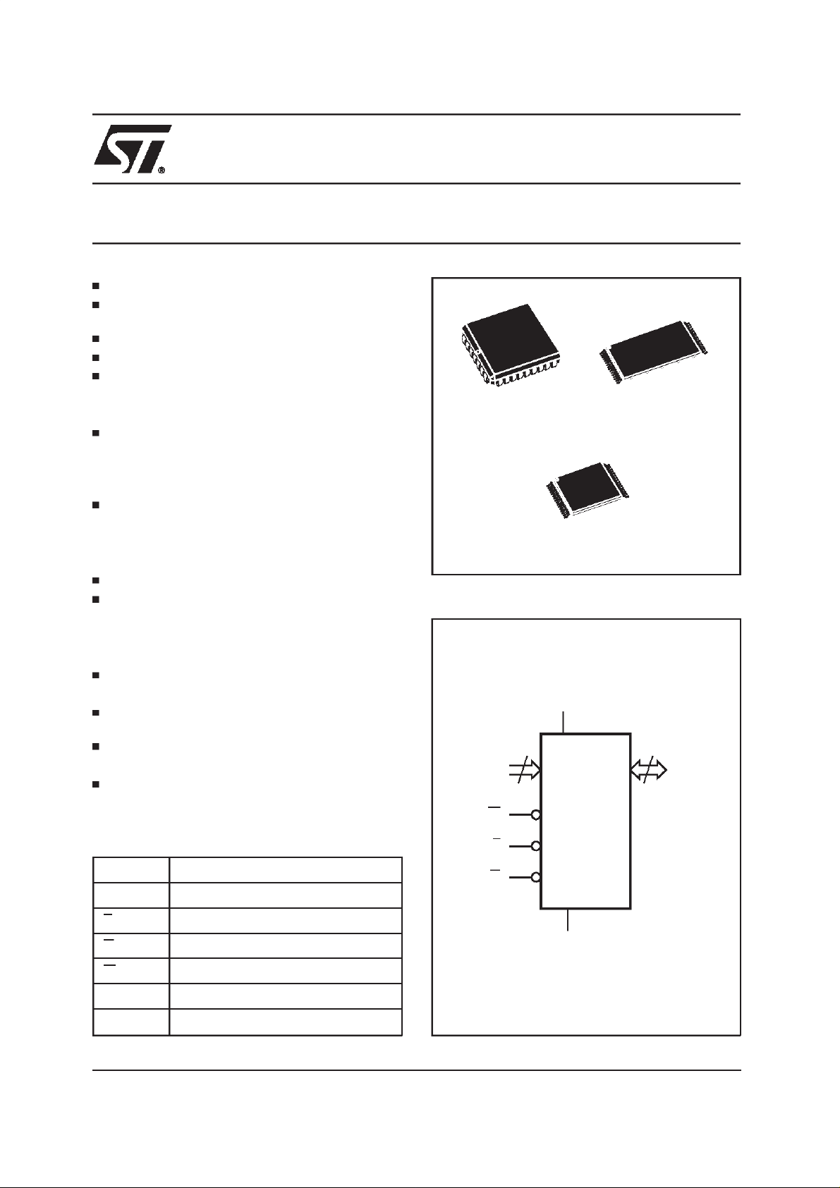
PLCC32 (K) TSOP32 (N)
TSOP32 (NZ)
8 x 14mm
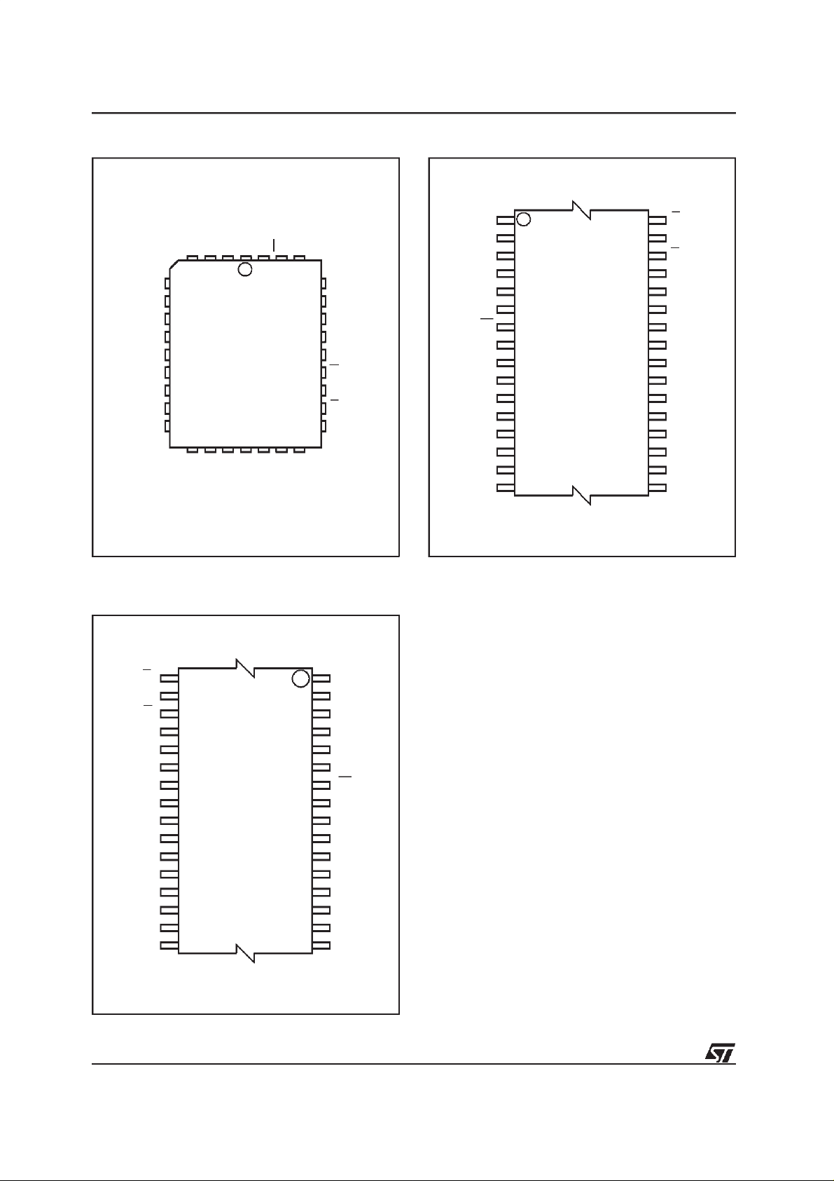
Figure 1. LogicDiagram
V
CC
19
A0-A18
W
E
M29W040
8 x 20mm
8
DQ0-DQ7
A0-A18 Address Inputs
DQ0-DQ7 Data Input / Outputs
E Chip Enable
G Output Enable
W Write Enable
V
CC
V
SS
November 1999 1/31
This is information ona product still in productionbutnot recommendedfor new designs.
Supply Voltage
Ground
G
V
SS
AI02074
M29W040
Figure 2A. LCC Pin Connections
CC
A18
32
DQ3
V
DQ4
W
DQ5
A7
A6
A5
A4
A3
A2
A1
A0
DQ0
A16
A12
A15
1
9
M29W040
DQ1
DQ2
V
17
SS
A17
25
DQ6
A14
A13
A8
A9
A11
G
A10
E
DQ7
AI02075
Figure 2B. TSOP Pin Connections
A11 G
A13
A14
A17
V
CC
A18
A16
A15
A12
1
A9
A8
W
8
M29W040
(Normal)
9
A7
A6
A5
A4 A3
16 17
32
25
24
AI02076
A10
E
DQ7
DQ6
DQ5
DQ4
DQ3
V
SS
DQ2
DQ1
DQ0
A0
A1
A2
Figure 2C. TSOP Reverse Pin Connections DESCRIPTION
The M29W040is a non-volatilememory that may
be erased electrically at the block level, and programmed Byte-by-Byte.
The interface is directly compatible with most microprocessors. PLCC32,TSOP32(8x 20mm)and
TSOP32(8 x 14mm)packagesare available.Both
normal and reverse pin outs are available for the
TSOP32(8 x 20mm) package.
Organisation
TheFlashMemoryorganisationis512Kx8 bitswith
Address lines A0-A18 and Data Inputs/Outputs
DQ0-DQ7. Memory control is provided by Chip
Enable,Output EnableandWrite Enable Inputs.
Erase and Program are performed through the
internal Program/EraseController(P/E.C.).
DataOutputsbits DQ7 and DQ6 provide pollingor
togglesignals duringAutomaticProgram or Erase
to indicate the Ready/Busy state of the internal
Program/EraseController.
MemoryBlocks
Erasure of the memory is in blocks. There are 8
uniform blocks of 64 Kbytes each in the memory
A10
DQ7
DQ6
DQ5
DQ4
DQ3
V
SS
DQ2
DQ1
DQ0
A0
A1
A2
1
E
8
9
16 17
M29W040
(Reverse)
32
25
24
AI02077
A11G
A9
A8
A13
A14
A17
W
V
CC
A18
A16
A15
A12
A7
A6
A5
A4A3
address space. Each block can be programmed
and erased over 100,000 cycles. Each uniform
2/31
M29W040
Table2. AbsoluteMaximum Ratings
Symbol Parameter Value Unit
T
A
T
BIAS
T
STG
(2)
V
IO
V
CC
(2)
V
A9
Notes:
1. Except for the rating ”Operating TemperatureRange”, stresses above those listed in theTable ”Absolute Maximum Ratings”
may cause permanent damage to the device. These are stressratings only and operation of the device at these or any other
conditions above those indicated in the Operating sections of this specification is not implied. Exposure to Absolute Maximum
Rating conditions for extended periods may affect device reliability.Refer also to the STMicroelectronicsSURE Program and other
relevant quality documents.
2. Minimum Voltage may undershoot to–2V during transition and for less than 20ns.
3. Depends on range.
Ambient Operating Temperature
TemperatureUnder Bias –50 to 125 °C
Storage Temperature –65 to 150
Input or OutputVoltages –0.6 to 5 V
Supply Voltage –0.6 to 5 V
A9 Voltage –0.6 to 13.5 V
block may separately be protected and unprotected against program and erase. Block erasure
may be suspended, while data is read from other
blocks of the memory,and then resumed.
Bus Operations
Seven operationscan be performed by the appropriate bus cycles, Read Array, Read Electronic
Signature,OutputDisable, Standby,ProtectBlock,
Unprotect Block, and Write the Command of an
Instruction.
Command Interface
Command Bytes can be written to a Command
Interface(C.I.) latch to perform Reading (from the
Array or Electronic Signature), Erasure or Programming. For added data protection, command
executionstarts after 4 or 6 commandcycles. The
first, second, fourth and fifth cycles are used to
input a code sequenceto the CommandInterface
(C.I.).Thissequenceis equal for allP/E.C. instructions. Command itself and its confirmation - if it
applies - are given on the third and fourth or sixth
cycles.
Instructions
Eight instructions are defined to perform Reset,
Read Electronic Signature, Auto Program, Block
Auto Erase, Chip Auto Erase, Block Erase Suspend, BlockErase Resumeand Power Down. The
internalProgram/EraseController(P/E.C.)handles
(1)
(3)
–40 to 85
instructionsandprovidesDataPolling,Toggle,and
Statusdata to indicatecompletionof Programand
EraseOperations.
Instructionsare composed of up to six cycles.The
firsttwocycles input a code sequenceto theCommand Interface which is common to all P/E.C.
instructions (see Table 7 for Command Descriptions). The third cycleinputs the instruction set up
command instruction to the Command Interface.
SubsequentcyclesoutputSignature,BlockProtection or the addressed data for Read operations.
For addeddataprotection,the instructionsfor program,and blockor chiperase require further commandinputs. Fora Programinstruction,the fourth
commandcycleinputsthe addressand data to be
programmed. For an Erase instruction (block or
chip),the fourthand fifthcyclesinputa furthercode
sequence before the Erase confirm command on
the sixth cycle. Byte programming takes typically
12µs while erase is performed in typically1.5 second.
Erasureof a memory block may be suspended,in
order to read data from another block, and then
resumed.Data Polling,Toggleand Errordata may
be read at any time,includingduring the programming or erase cycles, to monitor the progress of
the operation.When poweris firstapplied or ifV
fallsbelow V
,thecommandinterfaceis resetto
LKO
ReadArray.
all timingandverificationof theProgramandErase
C
°
C
°
CC
3/31
M29W040
Table3. Operations
Operation E G W DQ0 - DQ7
Read V
Write V
Output Disable V
Standby V
Note:
X=V
or V
IL
IH
Table4. ElectronicSignature
IL
IL
IL
IH
V
IL
V
IH
V
IH
V
IH
V
IL
V
IH
X X Hi-Z
Data Output
Data Input
Hi-Z
Code E G W A0 A1 A6 A9
Manufact. Code V
Device Code V
IL
IL
V
IL
V
IL
V
IH
V
IH
V
IL
V
IH
V
IL
V
IL
Table5. BlockProtectionStatus
Code E G W A0 A1 A6 A16 A17 A18
Protected Block V
Unprotected Block V
Note: SA = Address of block being checked
DEVICEOPERATION
Signal Descriptions
AddressInputs (A0-A18). Theaddress inputs for
the memoryarrayare latchedduring awrite operation. The A9 address input is used also for the
Electronic Signature read and BlockProtect verification. When A9 is raised to V
Manufacturer Code, Read Device Code or Verify
BlockProtectionisenableddependingon thecombinationof levelson A0, A1 and A6. WhenA0, A1
and A6areLow,the ElectronicSignatureManufacturer codeis read,when A0is Highand A1 and A6
are Low,the Device code is read, and when A1 is
High and A0 and A6 are low, the Block Protection
Status with protect/unprotectalgorithm is read for
the blockaddressedbyA16, A17, A18.
Data Input/Outputs(DQ0-DQ7).Thedata inputis
a byteto be programmedor a commandwrittento
the C.I. Both are latched when ChipEnable E and
WriteEnable W areactive.The dataoutput isfrom
the memory Array, the Electronic Signature, the
Data Polling bit (DQ7), the Toggle Bit (DQ6), the
Error bit (DQ5) or the Erase Timer bit (DQ3). Ouputs are valid when Chip Enable E and Output
EnableG are active.The outputis highimpedance
V
V
V
V
IL
IL
IH
IL
V
V
IL
IL
V
IH
IL
V
IH
IL
V
V
IH
IL
when the chip is deselected or the outputs are
disabled.
Chip Enable (E). The Chip Enable activates the
memorycontrol logic, input buffers, decoders and
senseamplifiers.EHighdeselectsthememoryand
reduces the power consumption to the standby
, either a Read
ID
level. E can also be used to control writing to the
command registerand tothe memoryarray,while
W remains at a low level. Addresses are then
latchedon thefallingedgeofEwhiledataislatched
on the rising edge of E. The Chip Enable must be
forcedto V
OutputEnable (G). The OutputEnable gates the
outputs through the data buffers during a read
operation. G must be forced to V
BlockProtect and Block Unprotectoperations.
WriteEnable(W).This inputcontrolswritingto the
CommandRegisterandAddressandDatalatches.
Addressesare latchedon thefallingedgeofW, and
DataInputs are latched on the rising edgeof W.
V
CC
operations(Read, Program and Erase).
V
SS
measurements.
Other
Addresses
V
V
V
IL
IL
ID
V
ID
Don’t Care 20h
Don’t Care E3h
Other
Addresses
DQ0 - DQ7
DQ0 - DQ7
SA SA SA Don’t Care 01h
SA SA SA Don’t Care 00h
during Block Unprotectoperations.
ID
level during
ID
Supply Voltage. The power supply for all
Ground. VSSis the reference for all voltage
4/31
M29W040
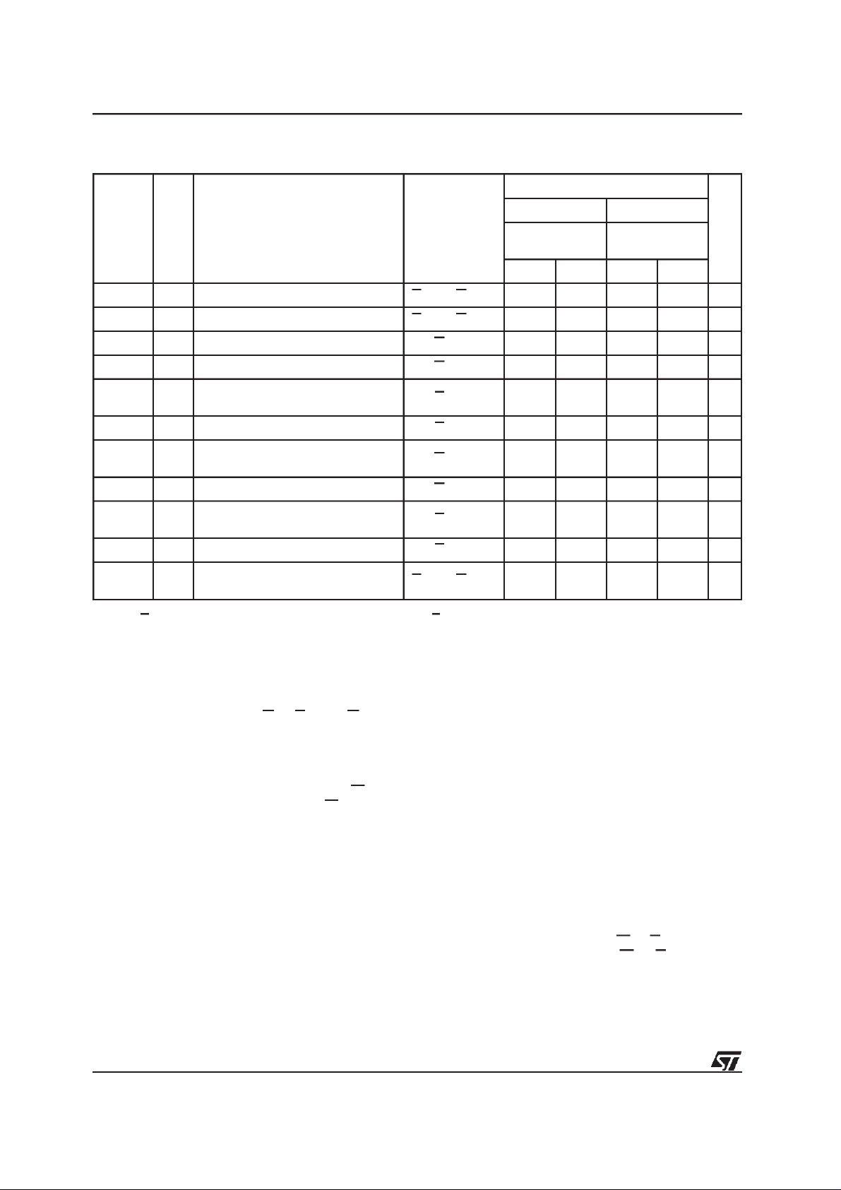
Table6. Instructions
(1)
Mne. Instr. Cyc. 1st Cyc. 2nd Cyc. 3rd Cyc. 4th Cyc. 5th Cyc. 6th Cyc. 7th Cyc.
RST
Read Array/
(3,9)
Reset
Addr.
1+
Data F0h
Addr.
3+
(2,6)
(2,6)
X
Read Memory Array until a new write cycle is initiated.
5555h 2AAAh 5555h
Read Memory Array until a new write
cycle is initiated.
Data AAh 55h F0h
(2,6)
Addr.
5555h 2AAAh 5555h
Data AAh 55h 90h
(2,6)
Addr.
5555h 2AAAh 5555h
Read Electronic Signature until a new
write cycle is initiated. See Note 4.
Read Block Protection untila new write
cycle is initiated. See Note 5.
RSIG
RBP
Read
(3)
Electronic
Signature
Read Block
(3)
Protection
3+
3+
Data AAh 55h 90h
Program
Address
Program
Data
Read Data Pollingor Toggle Bit
until Program completes.
Block
Address
Additional
Block
PG Program 4
BE Block Erase 6
(2,6)
Addr.
5555h 2AAAh 5555h
Data AAh 55h A0h
(2,6)
Addr.
5555h 2AAAh 5555h 5555h 2AAAh
(7)
Data AAh 55h 80h AAh 55h 30h 30h
(2,6)
CE Chip Erase 6
Addr.
5555h 2AAAh 5555h 5555h 2AAAh 5555h
Data AAh 55h 80h AAh 55h 10h
(2,6)
ES
Erase
Suspend
Addr.
1
X
Read until Togglestops, then read all the data needed from any
uniform block(s) not being erased then Resume Erase.
Data B0h
(2,6)
ER
Erase
Resume
Addr.
1
X
Read Data Pollingor ToggleBit until Erase completes or Erase
is suspended another time
Data 30h
(2,6)
PD
(10)
Power
Down
Addr.
1
5555h
Puts the memory in Power Down mode where power
consumption is reduced to typically less than 1µA
Data 20h
Notes:
1. Command not interpreted in this table will default to read array mode.
2. X = Don’tCare.
3. The first cycle ofthe RST,RBP or RSIG instruction is followed by read operations to read memory array,Status Register or
Electronic Signature codes. Any number of read cycles can occur after one command cycle.
4. Signature Addressbits A0,A1, A6 at V
Device code.
5. Protection Address: A0, A6 at V
Block Protectionstatus.
6. Address bits A15-A18are don’tcare for coded address inputs.
7. Optional, additional blocks addresses must be enteredwithin a 80µs delay afterlast write entry, timeout status can be verified
through DQ3 value. When full command is entered, read Data Polling or Toggle bit until Erase is completed or suspended.
8. Read Data Polling or Togglebit until Erase completes.
9. Await time of 5µs is necessary after a Reset command, if the memory is in a Block Erase or Power Down status, before
starting any operation.
10. Writing an RST command to theP/E.C. is mandatory prior to any new operation when the memory is in Power Down mode.
will output Manufacturer code (20h). Addressbits A0 at VIHandA1, A6 atVILwill output
IL
,A1atVIHand A16,A17, A18 within the uniform block tobe checked,will output the
IL
Note 8
5/31

M29W040
MemoryBlocks
The memoryblocks of the M29W040are shownin
Figure3. Thememory array is dividedin 8 uniform
blocks of 64 Kbytes. Each block can be erased
separately or any combination of blocks can be
erased simultaneously.The BlockEraseoperation
ismanagedautomaticallyby theP/E.C.Theoperation can be suspended in order to read from any
other block, and thenresumed.
Block Protectionprovides additionaldata security.
Each uniformblock can be separatelyprotectedor
unprotectedagainst ProgramorErase.BringingA9
and G to V
G and E to V
initiatesprotection,whilebringing A9,
ID
cancels the protection. The block
ID
affected during protection is addressed by the inputs on A16, A17, and A18. Unprotect operation
affectsall blocks.
Operations
Operationsare defined as specific bus cyclesand
signals which allow Memory Read, Command
Write,Output Disable, Standby,Read Status Bits,
Block Protect/Unprotect, Block Protection Check
and ElectronicSignatureRead.Theyare shownin
Tables 3, 4, 5.
Read. Read operations are used to output the
contents of the Memory Array,the Status Register
or the Electronic Signature. Both Chip Enable E
and OutputEnable G must be low in order to read
the output of the memory. The Chip Enable input
alsoprovidespowercontroland shouldbe usedfor
deviceselection.OutputEnable shouldbe usedto
gatedataontothe outputindependentof thedevice
selection.The data read dependson the previous
commandwritten to the memory (see instructions
RST and RSIG, and StatusBits).
Write.Writeoperationsare usedtogiveInstruction
Commandsto thememoryor to latchinput data to
be programmed.Awrite operationis initiatedwhen
Chip Enable E is Low and Write Enable W is Low
with OutputEnableG High.Addressesare latched
onthefallingedge ofWor Ewhicheveroccurslast.
CommandsandInputDataarelatchedon therising
edge of W or E whicheveroccurs first.
OutputDisable. Thedataoutputsare highimpedance whenthe OutputEnable G is High withWrite
EnableW High.
Standby. The memory is in standby when Chip
Enable E is High and Program/Erase Controller
P/E.C. is Idle. The power consumptionis reduced
to the standby level and the outputs are high impedance, independent of the Output Enable G or
WriteEnable W inputs.
AutomaticStandby. After 150ns of inactivity and
when CMOS levels are driving the addresses,the
chip automaticallyenters a pseudo standbymode
where consumption is reduced to the CMOS
standby value, while outputs are still driving the
bus.
Power Down. When the PD command is written
to the P/E.C. the memory enters a power down
statuswhere the power consumptionis reducedto
(typicallyless than 1.0µA).
I
CC6
Electronic Signature. Two codes identifying the
manufacturer andthe devicecanbe read fromthe
memory,themanufacturer’scodefor STMicroelectronics is 20h, and the device code is E3h for the
M29W040. These codes allow programming
equipment or applicationsto automatically match
theirinterfaceto thecharacteristicsof theparticular
manufacturer’s product. TheElectronicSignature
is output by a Read operation when the voltage
applied to A9 is at V
and address inputs A1 and
ID
A6 are at Low. The manufacturer code is output
when the Address input A0 is Low and the device
codewhen thisinputis High.Other Addressinputs
are ignored. The codes are outputon DQ0-DQ7.
This is shown in Table4.
The ElectronicSignature can alsobe read, without
raisingA9 to V
by givingthe memory the instruc-
ID
tion RSIG (see below).
6/31
Figure 3. MemoryMap and Block AddressTable
M29W040
A18
AI01362B
A17
1
1 64K Bytes Block
1
1
0
0
001
000
A16
1
1
0
0
1
1
1
0
1
0
1
0
Block Protection. Each uniform block can be
separately protected against Program or Erase.
Block Protectionprovides additionaldata security,
as it disablesall programoreraseoperations.This
mode is activated when both A9 and G are set to
and the block address is applied on A16-A18.
V
ID
Block Protection is programmed using a Presto F
programlike algorithm.Protectionisinitiatedon the
edgeofWfallingtoV
the edge of W rising to V
.Thenafteradelayof 100µs,
IL
ends the protection
IH
operation.Protectionverify is achievedby bringing
G, E andA6 to V
while W is at VIHand A9 at VID.
IL
Undertheseconditions,readingthedataoutputwill
yield 01h if the block defined by the inputs on
A16-A18 is protected. Any attempt to program or
erase a protected block will be ignored by the
device.
Any protected block can be unprotected to allow
updating of bit contents. All blocks must be protected before an unprotect operation. Block Unprotect is activatedwhen A9, G and E are at V
ID
The addressesinputs A6,A12, A16 mustbe maintainedatV
.BlockUnprotectis performedthrough
IH
a Presto F Erase like algorithm. Unprotect is initiated by the edgeof W falling to V
of 10ms, the edge of W rising to V
. After a delay
IL
will end the
IH
unprotection operation. Unprotect verify is
achieved by bringing G and E to V
while A6 and
IL
64K Bytes Block
64K Bytes Block
64K Bytes Block
64K Bytes Block
TOP
ADDRESS
7FFFFh
6FFFFh
5FFFFh
4FFFFh
3FFFFh
2FFFFh
1FFFFh
0FFFFh
BOTTOM
ADDRESS
70000h
60000h
50000h
40000h
30000h
20000h
10000h
00000h
Table7. Commands
Hex Code Command
10h Chip Erase Confirm
20h Power Down
30h Block Erase Resume/Confirm
50h Reserved
80h Set-up Erase
Read Electronic Signature/
Block Protection Status
and A9 at VID. In these conditions,
IH
.
90h
A0h Program
B0h Erase Suspend
F0h Read Array/Reset
W are at V
reading the output data will yield 00h if the block
defined by the inputs on A16-A18has been successfullyunprotected.AllcombinationsofA16-A18
mustbe addressedin orderto ensurethatallof the
8 uniform blocks have been unprotected. Block
ProtectionStatus is shownin Table5.
7/31
M29W040
Table8. Status Register
DQ Name Logic Level Definition Note
’1’ Erase Complete
Data
7
Polling
’0’ Erase on going
DQ Program Complete
DQ Program on going
Indicates the P/E.C. status, check during
Program or Erase, and on completion
before checking bits DQ5 for Program or
Erase Success.
’-1-0-1-0-1-0-1-’ Erase or Program ongoing Successive read output complementary
6 ToggleBit
5 ErrorBit
4
Erase
3
TimeBit
2 Reserved
1 Reserved
0 Reserved
Note:
Logic level ’1’ is High, ’0’ is Low.-0-1-0-0-0-1-1-1-0- represent bitvalue in successive Read operations.
’-0-0-0-0-0-0-0-’
’-1-1-1-1-1-1-1-’
’1’ Program or Erase Error
’0’ Program or Erase on going
’1’
’0’
’1’ Erase TimeoutPeriod Expired P/E.C. Erase operation has started. Only
’0’
Instructionsand Commands
The Command Interface (C.I.) latches commands
written to the memory. Instructions are made up
from one or more commands to perform Read
Array/Reset, Read Electronic Signature, Power
Down, Block Erase, Chip Erase, Program, Block
Erase Suspend and Erase Resume. Commands
are made of address and data sequences. Addresses are latched on the falling edge of W or E
and data is latched on the rising of W or E. The
instructionsrequire from 1 to 6 cycles, the first or
first three of which are always write operations
used toinitiatethecommand.Theyarefollowed by
either further write cyclesto confirmthe first command orexecutethecommandimmediately.Command sequencing must be followed exactly. Any
invalid combination of commands will reset the
device to Read Array. The increased number of
cycles has been chosen to assure maximum data
security.Commands are initialised by two precedingcoded cycleswhich unlocktheCommandInterface.In addition,forErase,command confirmation
is again preceededby the two codedcycles.
P/E.C. statusis indicatedduringcommandexecutionby DataPolling onDQ7, detectionof Toggleon
Program (’0’ on DQ6)
Complete
Erase or Program
(’1’ on DQ6) Complete
Erase Timeout Period on
going
DQ6, or Error on DQ5 and Erase TimerDQ3 bits.
Any read attempt during Program or Erase commandexecutionwillautomaticallyoutputthosefour
bits.TheP/E.C. automaticallysetsbitsDQ3,DQ5,
DQ6 and DQ7. Other bits (DQ0, DQ1, DQ2 and
DQ4) are reserved for future use and should be
masked.
Data Polling bit (DQ7). When Programmingoperations are in progress, this bit outputs the complement of the bit being programmed on DQ7.
DuringErase operation,it outputsa ’0’. After completionof the operation,DQ7 will output the bit last
programmed or a ’1’ after erasing. Data Polling is
valid only effective duringP/E.C. operation,that is
after the fourth W pulse for programming or after
the sixth W pulse for Erase. It mustbe performed
at theaddressbeing programmedor at an address
within the block being erased. If the byte to be
programmedbelongsto aprotectedblock thecommand is ignored. If all the blocks selected for erasure are protected, DQ7 will set to ’0’ for about
100µs, and then return to previous addressed
memory data. See Figure 9 for the Data Polling
flowchartandFigure10 for the Data Polling waveforms.
data on DQ6 while Programming or Erase
operations are going on. DQ6 remain at
constant level when P/E.C. operations are
completed or Erase Suspend is
acknowledged.
This bit is set to ’1’ if P/E.C. has exceded
the specified time limits.
possible command entry is Erase Suspend
(ES). An additionalblock to be erased in
parallel can be entered to the P/E.C.
8/31
M29W040
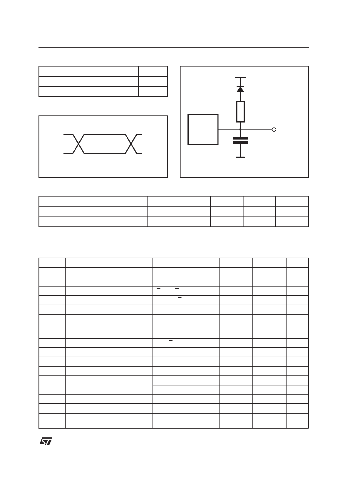
Table9. ACMeasurement Conditions
Input Rise and Fall Times
≤
10ns
Figure5. AC TestingLoad Circuit
0.8V
Input Pulse Voltages 0 to 3V
Input and Output Timing Ref. Voltages 1.5V
Figure 4. AC TestingInputOutput Waveform
3V
1.5V
0V
AI01417
Table10. Capacitance
(1)
(TA=25°C, f = 1 MHz)
DEVICE
UNDER
TEST
CLincludes JIG capacitance
1N914
3.3kΩ
CL= 30pF or 100pF
Symbol Parameter Test Condition Min Max Unit
C
IN
C
OUT
Note:
1. Sampled only,not 100% tested.
Input Capacitance VIN=0V 6 pF
Output Capacitance V
=0V 12 pF
OUT
OUT
AI01968
Table11. DC Characteristics
=0 to 70°C, –20 to 85°C or –40 to85°C; VCC= 2.7V to 3.6V)
(T
A
Symbol Parameter Test Condition Min Max Unit
V
I
I
I
I
I
I
V
V
I
LI
I
LO
CC1
CC2
CC3
CC4
CC5
CC6
V
V
OL
OH
V
I
ID
LKO
Input Leakage Current 0V ≤ VIN≤ V
Output LeakageCurrent 0V ≤ V
OUT
≤ V
CC
CC
Supply Current (Read) E= VIL,G=VIH, f = 6MHz 20 mA
Supply Current (Standby) TTL E = V
Supply Current (Standby) CMOS E = V
Supply Current (Program or Erase)
Byte Program,
Block Erase
IH
0.2V 50
±
CC
Supply Current Chip Erase in progress 40 mA
Power Down Current E = V
Input Low Voltage –0.5 0.8 V
IL
Input High Voltage 0.7 V
IH
0.2V 5
±
CC
CC
Output Low Voltage IOL= 2mA 0.45 V
I
= –100µAV
Output High Voltage CMOS
A9 Voltage (Electronic Signature) 11.5 12.5 V
ID
A9 Current (Electronic Signature) A9 = V
OH
= –2.0mA 0.85 V
I
OH
ID
Supply Voltage (Erase and
Program lock-out)
–0.4 V
CC
CC
1.9 2.2 V
±1 µA
±1 µA
0.2 mA
20 mA
VCC+ 0.5 V
50 µA
A
µ
A
µ
V
9/31
M29W040
Table12A. Read AC Characteristics
=0 to 70°C, –20 to 85°C or –40 to85°C)
(T
A
Symbol Alt Parameter Test Condition
t
t
AVAV
t
AVQVtACC
(1)
t
ELQX
(2)
t
ELQV
(1)
t
GLQX
(2)
t
GLQV
t
EHQX
(1)
t
EHQZ
t
GHQX
(1)
t
GHQZ
t
AXQX
Notes: 1. Sampled only,not 100% tested.
2. G may be delayed by up to t
Address Validto Next Address Valid E = VIL,G=V
RC
Address Validto Output Valid E = VIL,G=V
tLZChip Enable Low toOutput Transition G = V
t
Chip Enable Low to Output Valid G = V
CE
Output Enable Low to Output
t
OLZ
Transition
t
Output Enable Low to OutputValid E = V
OE
Chip Enable High to Output
t
OH
Transition
E=V
G=V
tHZChip Enable High to Output Hi-Z G = V
Output Enable High to Output
t
OH
Transition
E=V
tDFOutput Enable High to Output Hi-Z E = V
Address Transition to Output
t
OH
Transition
ELQV-tGLQV
afterthe falling edge of E without increasing t
E=V
IL
IL
IL
IL
IL
IL
IL
IL
IL
,G=V
M29W040
-100 -120
= 3.3V±0.3V
V
CC
C
= 30pF
L
= 3.3V±0.3V
V
CC
Unit
Min Max Min Max
100 120 ns
IL
IL
100 120 ns
00ns
100 120 ns
00ns
40 50 ns
00ns
20 30 ns
00ns
20 30 ns
00ns
IL
.
ELQV
Toggle bit (DQ6). When Programmingoperations
are in progress, successiveattempts to read DQ6
will output complementary data. DQ6 will toggle
following toggling of either G or E when G is low.
The operation is completed when two successive
reads yield the same output data. The next read
will output the bit last programmed or a ’1’ after
erasing. Thetogglebit is validonlyeffectiveduring
P/E.C. operations, that is after the fourth W pulse
for programming or after the sixth W pulse for
Erase. If the byte to be programmed belongs to a
protectedblockthe commandwill beignored.If the
blocksselectedfor erasureare protected,DQ6will
toggle for about 100µs and then return back to
Read. See Figure 11 for ToggleBit flowchart and
Figure 12 for ToggleBit waveforms.
Error bit (DQ5). This bit is set to ’1’ by the P/E.C
when there is a failure ofbyte programming,block
erase, or chip erase that results in invalid data
being programmedin thememory block.In caseof
error in block erase or byte program, the block in
which the error occured or to which the pro-
10/31
grammedbyte belongs,must be discarded. Other
blocksmaystillbeused.Errorbitresetsafter Reset
(RST) instruction. In case of success, the error bit
will set to ’0’ during Program or Erase and to valid
data afterwrite operation is completed.
Erase Timer bit (DQ3). Thisbit is set to ’0’by the
P/E.C. when the last Block Erase command has
been entered to the Command Interface and it is
awaiting the Erase start. When the erase timeout
period is finished, after 80 to 120µs, DQ3 returns
backto ’1’.
Coded Cycles. The two coded cycles unlock the
Command Interface. They are followed by a command input or a comand confirmation.The coded
cycles consist of writing the data AAh at address
5555hduringthefirstcycleanddata55hat address
2AAAh during the second cycle. Addresses are
latched on the fallingedge of W or E while data is
latched on the rising edge of W or E. The coded
cycles happen on first and second cycles of the
commandwrite or on the fourth and fifth cycles.
 Loading...