

Low Voltage Single Supply Flash Memory
■ SINGLE 2.7 to3.6V SUPPLY VOLTAGEfor
PROGRAM, ERASE and READ OPERATIONS
■ ACCESS TIME: 55ns
■ PROGRAMMING TIME
–10µs by Byte typical
■ 7 MEMORY BLOCKS
– 1 Boot Block (Top or Bottom Location)
– 2 Parameter and 4 Main Blocks
■ PROGRAM/ERASE CONTROLLER
– Embedded Byte Program algorithm
– Embedded Multi-Block/Chip Erase algorithm
– Status Register Polling and Toggle Bits
■ ERASE SUSPEND and RESUME MODES
– Read and Program another Block during
Erase Suspend
■ UNLOCK BYPASS PROGRAM COMMAND
– Faster Production/Batch Programming
■ LOW POWER CONSUMPTION
– Standby andAutomatic Standby
■ 100,000 PROGRAM/ERASE CYCLES per
BLOCK
■ 20 YEARS DATA RETENTION
– Defectivity below 1 ppm/year
■ ELECTRONIC SIGNATURE
– Manufacturer Code:20h
– Top Device Code M29W022BT: C4h
– Bottom DeviceCode M29W022BB: C3h
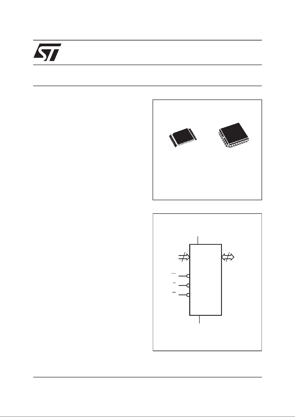
M29W022BT
M29W022BB
2 Mbit (256Kb x8, Boot Block)
TSOP32 (NZ)
8 x 14mm
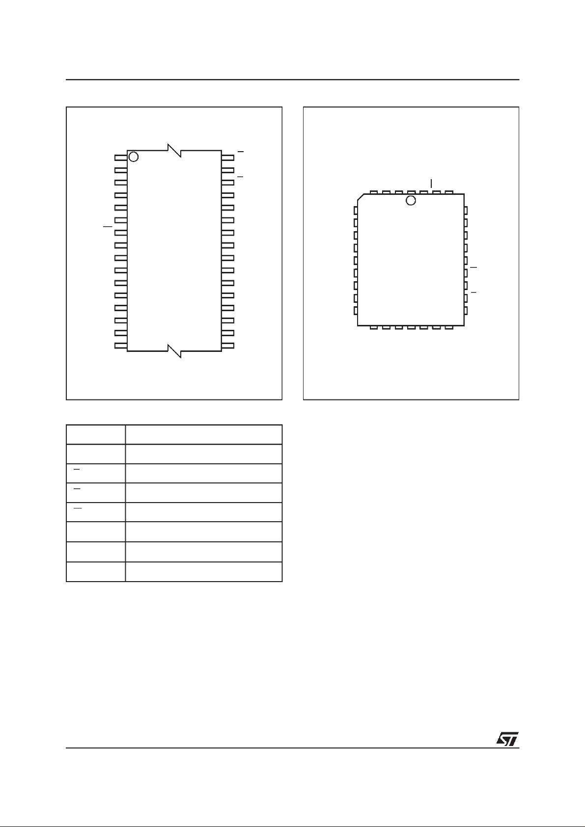
Figure 1. Logic Diagram
V
CC
18
A0-A17
W
E
G
M29W022BT
M29W022BB
PLCC32 (K)
8
DQ0-DQ7
V
SS
AI02971
1/20March 2000
M29W022BT, M29W022BB
Figure 2. TSOP Connections
A11 G
A9
A8
A13
A14
A17
V
CC
NC
A16
A15
A12
A7
A6
A5
A4 A3
1
W
8
M29W022BT
M29W022BB
9
16 17
32
25
24
AI02970
A10
E
DQ7
DQ6
DQ5
DQ4
DQ3
V
SS
DQ2
DQ1
DQ0
A0
A1
A2
Figure 3. PLCC Connections
A16
A7
A6
A5
A4
A3
A2
A1
A0
DQ0
A12
9
DQ1
NC
V
17
SS
1
32
DQ3
V
DQ4
A15
M29W022BT
M29W022BB
DQ2
CC
W
DQ5
A17
25
DQ6
A14
A13
A8
A9
A11
G
A10
E
DQ7
AI03045
Table 1. Signal Names
A0-A17 Address Inputs
DQ0-DQ7 Data Inputs/Outputs
E Chip Enable
G Output Enable
W Write Enable
V
CC
V
SS
NC Not Connected Internally
Supply Voltage
Ground
SUMMARY DESCRIPTION
The M29W022B is a 2 Mbit (256Kb x8) non-volatile memory that can be read, erased and reprogrammed. These operations can be performed
using a single lowvoltage (2.7 to 3.6V) supply. On
power-up the memory defaults to its Read mode
where itcan be read in the same wayas aROM or
EPROM.
The memory is divided into blocks that can be
erased independently so it is possible to preserve
valid datawhile old datais erased. Eachblock can
be protected independently to prevent accidental
Program or Erase commands from modifying the
memory. Program and Erase commands are written to the Command Interface of the memory. An
on-chip Program/Erase Controller simplifies the
process of programming orerasing the memoryby
taking care of all ofthe special operations that are
required to update thememory contents. The end
of a program or erase operation can be detected
and any error conditions identified. The command
set required to control the memory is consistent
with JEDEC standards.
The blocks in the memory are asymmetrically arranged,see Tables 3 and 4, Block Addresses.The
first or last 64 Kbytes have been divided into four
additional blocks.The 16 Kbyte Boot Block can be
used for small initialization code to start the microprocessor, the two 8 Kbyte Parameter Blocks can
be used for parameter storage and the remaining
32 Kbyte is a small MainBlock where the application may bestored.
Chip Enable, Output Enable and Write Enable signals control the bus operation of the memory.
They allow simple connection to most microprocessors, often without additional logic.
The memory is offered in a TSOP32 (8 x 14mm)
and PLCC32 packages and it is supplied with all
the bits erased (set to ’1’).
2/20
M29W022BT, M29W022BB
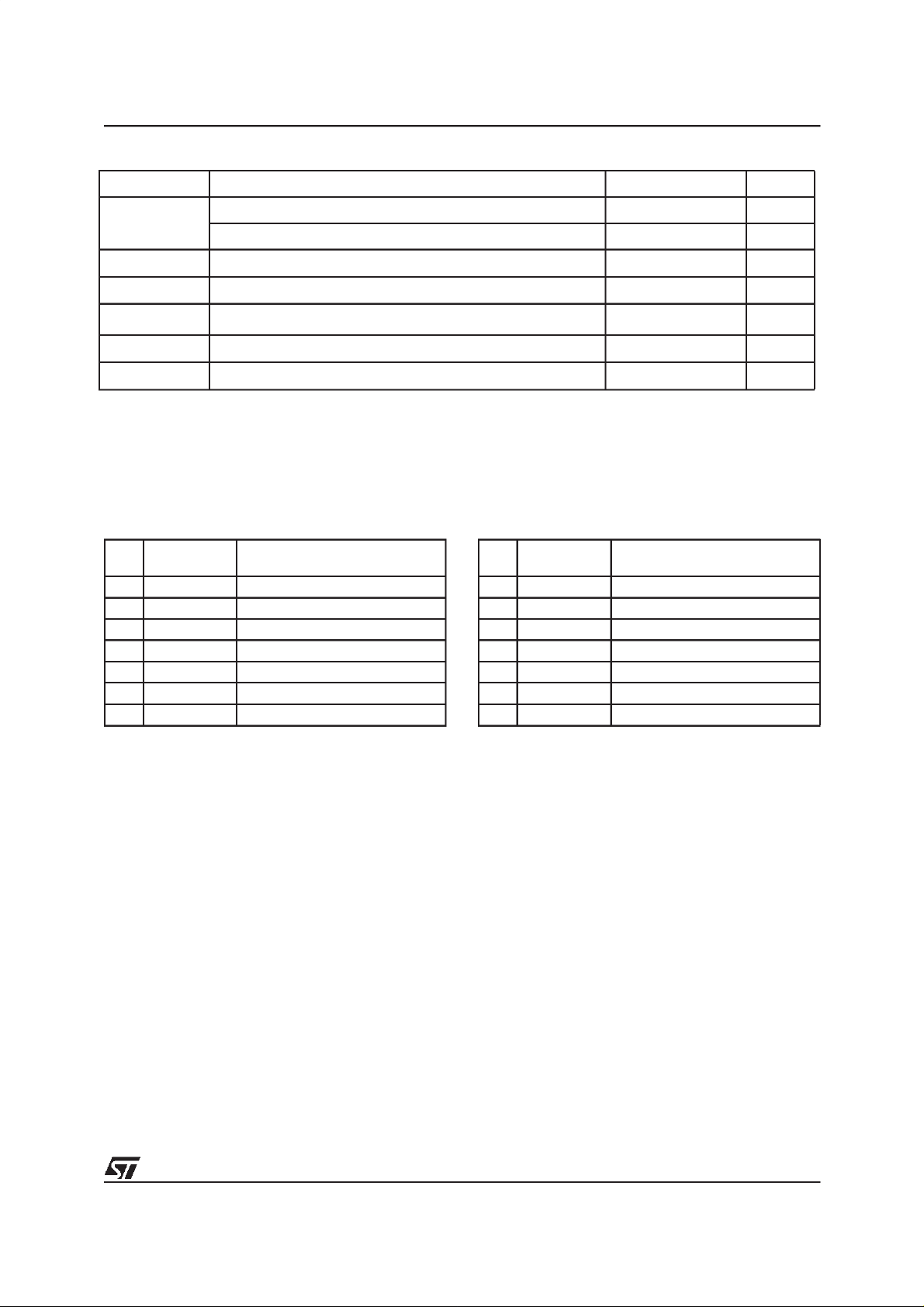
Table 2. Absolute Maximum Ratings
(1)
Symbol Parameter Value Unit
Ambient Operating Temperature (Temperature Range Option 1) 0 to 70 °C
T
A
T
BIAS
T
STG
(2)
V
IO
V
CC
V
ID
Note: 1. Except for the rating ”Operating Temperature Range”, stresses above those listed in the Table ”Absolute Maximum Ratings” may
cause permanent damage to the device. These are stress ratings only and operation of the device atthese or any other conditions
above those indicated in the Operating sections of this specification is not implied. Exposure to Absolute Maximum Rating conditions for extended periods may affect device reliability. Refer also to theSTMicroelectronics SURE Program and other relevant quality documents.
2. Minimum Voltage may undershoot to –2V during transition and for less than 20ns during transitions.
Table 3. Top Boot Block Addresses
M29W022BT
#
(Kbytes)
6 16 3C000h-3FFFFh
5 8 3A000h-3BFFFh
4 8 38000h-39FFFh
3 32 30000h-37FFFh
2 64 20000h-2FFFFh
1 64 10000h-1FFFFh
0 64 00000h-0FFFFh
Ambient Operating Temperature (Temperature Range Option 6) –40 to 85 °C
Temperature Under Bias –50 to 125 °C
Storage Temperature –65 to 150 °C
Input or Output Voltage –0.6 to 4 V
Supply Voltage –0.6 to 4 V
Identification Voltage –0.6 to 13.5 V
Table 4. Bottom Boot Block Addresses
M29W022BB
Size
Address Range
#
6 64 30000h-3FFFFh
5 64 20000h-2FFFFh
4 64 10000h-1FFFFh
3 32 08000h-0FFFFh
2 8 06000h-07FFFh
1 8 04000h-05FFFh
0 16 00000h-03FFFh
Size
(Kbytes)
Address Range
3/20

M29W022BT, M29W022BB
SIGNAL DESCRIPTIONS
See Figure 1, Logic Diagram, and Table 1, Signal
Names, forabriefoverview ofthesignalsconnected to this device.
Address Inputs (A0-A17). The Address Inputs
select thecells in the memoryarray to access during BusRead operations. During Bus Write operations they control the commands sent to the
Command Interface of the internal state machine.
Data Inputs/Outputs (DQ0-DQ7). The Data Inputs/Outputs outputthe data storedatthe selected
address during aBus Readoperation. During Bus
Write operations they represent the commands
sent tothe CommandInterfaceof the internal state
machine.
Chip Enable (E). The Chip Enable, E, activates
the memory, allowing BusRead and BusWriteoperations to be performed. When Chip Enable is
High, VIH, all other pins are ignored.
Output Enable (G). The Output Enable, G, controls the BusRead operation of the memory.
Write Enable (W). The Write Enable, W,controls
the Bus Write operation of the memory’s Command Interface.
VCCSupply Voltage. The VCCSupply Voltage
supplies the power for all operations (Read, Program, Eraseetc.).
The Command Interface is disabledwhen the V
CC
Supply Voltage is less than the Lockout Voltage,
V
. Thisprevents Bus Write operationsfrom ac-
LKO
cidentally damaging the data during power-up,
power-down and power surges. If the Program/
Erase Controller is programming or erasing during
this time then the operationaborts and the memory contents being altered will be invalid.
A 0.1µF capacitor should be connected between
the VCCSupply Voltage pin and the VSSGround
pin to decouple the current surges from the power
supply. ThePCB track widthsmust be sufficientto
carry the currents required during program and
erase operations,I
CC3
.
VSSGround. The VSSGroundis the reference for
all voltage measurements.
4/20
M29W022BT, M29W022BB
BUS OPERATIONS
There are fivestandard bus operations thatcontrol
the device. These are Bus Read, Bus Write, Output Disable,Standby andAutomatic Standby. See
Table 5,Bus Operations,for asummary. Typically
glitches of less than 5ns on Chip Enable or Write
Enable are ignored by the memory and do not affect busoperations.
Bus Read. Bus Read operations read from the
memory cells, or specific registers in the Command Interface. A valid Bus Read operation involves settingthe desired address on theAddress
Inputs, applying a Low signal, VIL, to Chip Enable
and Output Enable and keeping Write Enable
High, VIH. The Data Inputs/Outputs will output the
value, see Figure 8, Read Mode AC Waveforms,
and Table12, Read AC Characteristics, fordetails
of when the output becomes valid.
Bus Write. Bus Write operations write to the
Command Interface. A valid Bus Write operation
begins by setting the desired address on the Address Inputs. The Address Inputs are latched by
the CommandInterface on thefalling edge of Chip
Enable or Write Enable, whichever occurs last.
The Data Inputs/Outputs are latched by the Command Interface on the rising edge of Chip Enable
or WriteEnable, whicheveroccursfirst.Output Enable must remain High, VIH, during the whole Bus
Write operation. See Figures 9 and 10, Write AC
Waveforms, and Tables 13 and 14, Write AC
Characteristics, for details of the timing requirements.
Output Disable. The Data Inputs/Outputs are in
the high impedance state when Output Enable is
High, VIH.
Standby. When Chip Enable is High, VIH, the
memory enters Standby mode and the Data Inputs/Outputs pins are placed in the high-impedance state. To reduce the Supply Current to the
Standby Supply Current, I
, ChipEnable should
CC2
be held withinVCC± 0.2V.For the Standby current
level see Table 11, DC Characteristics.
During program or erase operations the memory
will continue to use the Program/Erase Supply
Current, I
, forProgramor Erase operationsun-
CC3
til the operation completes.
Automatic Standby. If CMOSlevels (VCC± 0.2V)
are used to drive the bus andthe bus is inactive for
150ns or more the memory enters Automatic
Standby where the internal Supply Current is reduced to the Standby Supply Current, I
CC2
. The
Data Inputs/Outputs will still output data if a Bus
Read operation is in progress.
Special Bus Operations
Additional bus operations can be performed to
read the Electronic Signature and also to apply
and remove Block Protection. These bus operations are intended for use by programming equipment and are not usually used in applications.
They require VIDto be applied to some pins.
Electronic Signature. The memory has two
codes, the manufacturer code and the device
code, that can be read to identify the memory.
These codes can be read by applying the signals
listed in Table 5, Bus Operations.
Block Protection and BlocksUnprotection. Each
block can be separately protected against accidental Program or Erase.Protected blocks canbe
unprotected to allow data to be changed. Block
Protection and Blocks Unprotection operations
must only be performed on programming equipment. For further information refer to Application
Note AN1122, Applying Protection and Unprotection to M29 Series Flash.
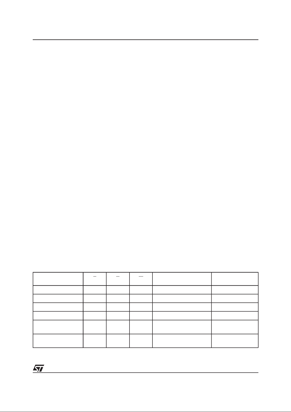
Table 5. Bus Operations
Operation E G W Address Inputs
Bus Read
Bus Write V
Output Disable
Standby
Read Manufacturer
Code
Read Device Code
Note: X = VILor VIH.
V
IL
IL
XV
V
IH
V
IL
V
IL
V
IL
V
IH
IH
X X X Hi-Z
V
IL
V
IL
Data
Inputs/Outp uts
V
V
V
V
V
Cell Address Data Output
IH
Command Address Data Input
IL
X Hi-Z
IH
A0 = VIL,A1=VIL,A9=VID,
IH
Others V
A0 = VIH,A1=VIL,A9=VID,
IH
Others V
or V
IL
IH
or V
IL
IH
20h
C4h (M29W022BT)
C3h (M29W022BB)
5/20

M29W022BT, M29W022BB
COMMAND INTERFACE
All Bus Write operations to the memory are interpreted by the Command Interface. Commands
consist of one or more sequential Bus Write operations. Failureto observe a valid sequence of Bus
Write operations will result in the memory returning to Readmode.The long command sequences
are imposed to maximize data security.
The commands are summarized in Table 6, Commands. Refer to Table 6 in conjunction with the
text descriptions below.
Read/Reset Command. The Read/Reset command returnsthe memory toits Read mode where
it behaves like a ROM or EPROM. It also resets
the errors in the Status Register. Either one or
three Bus Write operations can be used to issue
the Read/Reset command.
If the Read/Reset command is issued during a
Block Eraseoperation or followinga Programming
or Eraseerror then thememory will take upto 10µs
to abort. Duringthe abort period no valid data can
be read from the memory. Issuing a Read/Reset
command during a Block Erase operation will
leave invalid datain the memory.
Auto Select Command. The Auto Select command is used to read the Manufacturer Code, the
Device Code and the Block Protection Status.
Three consecutive Bus Write operations are required to issue the Auto Select command. Once
the Auto Select command is issued the memory
remains in Auto Select mode until another command is issued.
From the Auto Select mode the Manufacturer
Code can be read using a Bus Read operation
with A0 = VILand A1 = VIL. The other address bits
may be set to either VILor VIH. The Manufacturer
Code for STMicroelectronics is 20h.
The Device Code can be read using a Bus Read
operation with A0 = VIHand A1 = VIL. The other
address bits may be set to either VILor VIH.The
Device Code for the M29W022BT is C4h and the
M29W022BB is C3h.
The Block Protection Status of each block can be
read using a Bus Read operation with A0 = VIL,
A1 = VIH, and A13-A17 specifying the address of
the block. The otheraddress bits maybe set toeither VILor VIH. If the addressed block is protected
then 01his outputon the DataInputs/Outputs,otherwise 00h is output.
Program Command. The Program command
can be usedto program a value to one addressin
the memory array at a time. The command requires fourBus Writeoperations,the finalwriteoperation latchestheaddressand data in theinternal
state machine and starts the Program/Erase Controller.
If the address falls in a protected block then the
Program command is ignored, the data remains
unchanged. The Status Registerisnever read and
no errorcondition is given.
During the program operation the memory will ignore all commands. It is not possible to issue any
command to abort or pause the operation. Typical
program timesare given in Table 7.Bus Read operations during the program operation will output
the Status Register on the Data Inputs/Outputs.
See the section on the Status Register for more
details.
After the program operation has completed the
memory will return to the Read mode, unless an
error has occurred. When an error occurs the
memory will continue to output the Status Register. A Read/Reset command must be issued to reset the error condition and return to Read mode.
Note thatthe Programcommand cannotchange a
bit set at ’0’ back to ’1’. One of the Erase Commands must beused to setall the bits in ablock or
in the wholememory from ’0’ to ’1’.
Unlock Bypass Command. The Unlock Bypass
command is used in conjunction with the Unlock
Bypass Program commandto programthe memory. When the access time to the device is long (as
with some EPROM programmers) considerable
time saving can be made by using these commands. Three Bus Write operations are required
to issue the Unlock Bypass command.
Once the Unlock Bypass command has been issued the memory will only accept the Unlock Bypass Program command and the Unlock Bypass
Reset command. The memorycan be read as if in
Read mode.
Unlock Bypass Program Command. The Un-
lock Bypass Program command can be used to
program one address in memory at a time. The
command requires two Bus Write operations, the
final write operation latches the address and data
in the internal state machine and starts the Program/Erase Controller.
The Program operation using the Unlock Bypass
Program command behaves identically tothe Program operation using the Program command. A
protected block cannot be programmed; the operation cannot be aborted and theStatusRegister is
read. Errors must be reset using the Read/Reset
command, which leaves the device in Unlock Bypass Mode. See the Programcommand for details
on thebehavior.
Unlock Bypass Reset Command. The Unlock
Bypass Reset command can be used to return to
Read/Reset mode from Unlock Bypass Mode.
TwoBus Write operations are requiredtoissue the
Unlock Bypass Reset command.
6/20
 Loading...