

SGS Thomson Microelectronics M29F800AB70M1, M29F800AB, M29F800AT90N1, M29F800AT90M1, M29F800AT70N1 Datasheet
...
1/21
PRELIMINARY DATA
January 2000
This is preliminary information on a new product now in development or undergoing evaluation. Details are subject to change without notice.
M29F800AT
M29F800AB
8 Mbit (1Mb x8 or 512Kb x16, Boot Block)
Single Supply Flash Memory
■ SINGLE 5V±10% SUPPLY VOLTAGE for
PROGRAM, ERASE and READ OPERATIONS
■ ACCESS TIME: 70ns
■ PROGRAMMING TIME
–8µs per Byte/Word typical
■ 19 MEMORYBLOCKS
– 1 BootBlock (Top or Bottom Location)
– 2 Parameterand 16 Main Blocks
■ PROGRAM/ERASE CONTROLLER
– Embedded Byte/Word Program algorithm
– Embedded Multi-Block/Chip Erase algorithm
– Status Register Polling and Toggle Bits
– Ready/Busy OutputPin
■ ERASE SUSPEND and RESUME MODES
– Read and Programanother Block during
Erase Suspend
■ TEMPORARY BLOCK UNPROTECTION
MODE
■ LOW POWER CONSUMPTION
– Standby andAutomatic Standby
■ 100,000 PROGRAM/ERASE CYCLESper
BLOCK
■ 20 YEARS DATA RETENTION
– Defectivity below 1 ppm/year
■ ELECTRONIC SIGNATURE
– Manufacturer Code: 0020h
– M29F800ATDevice Code: 00ECh
– M29F800AB Device Code:0058h
44
1
TSOP48 (N)
12 x 20mm
SO44 (M)
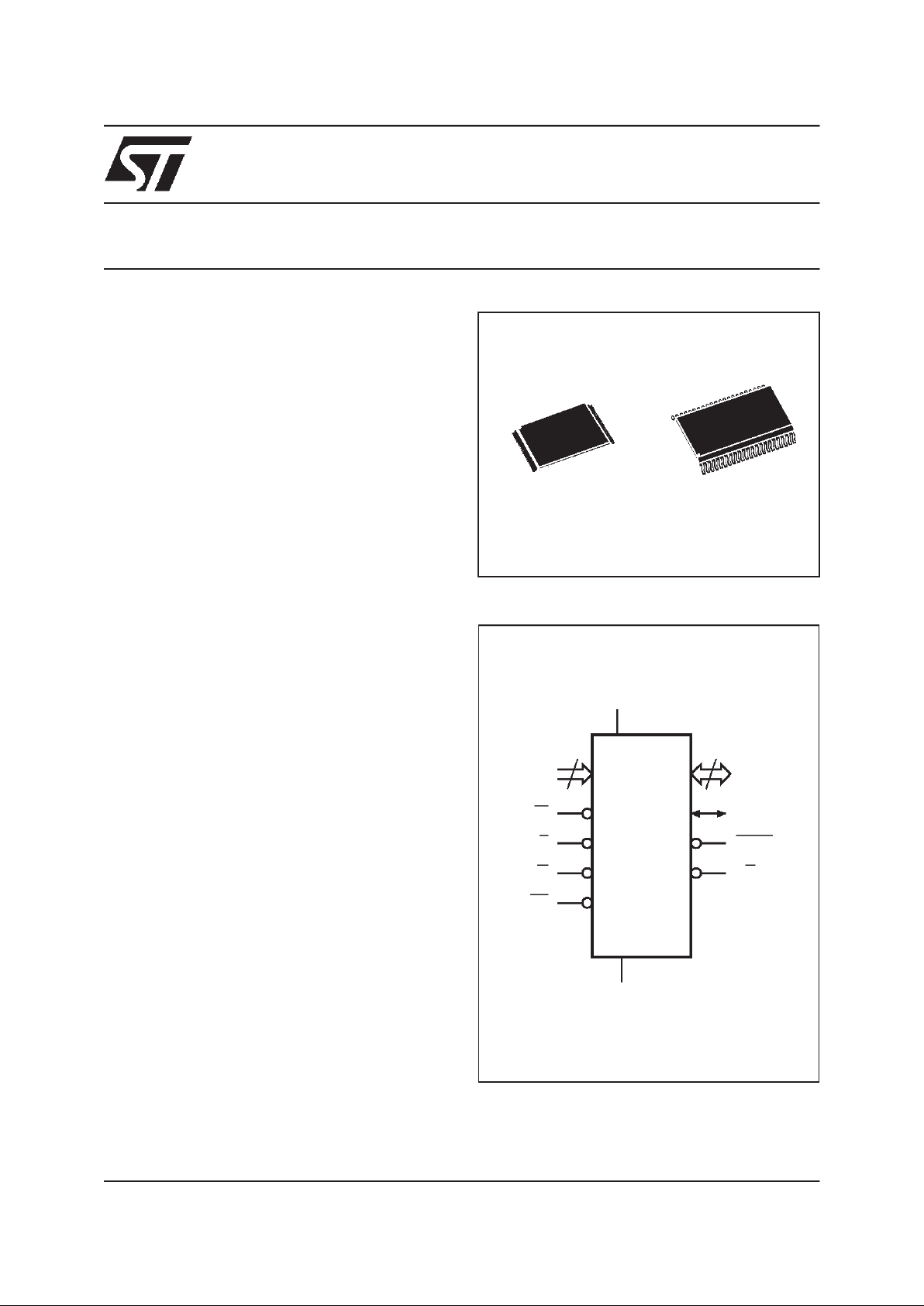
Figure 1. Logic Diagram
AI02198B
19
A0-A18
W
DQ0-DQ14
V
CC
M29F800AT
M29F800AB
E
V
SS
15
G
RP
DQ15A–1
BYTE
RB
M29F800AT, M29F800AB
2/21
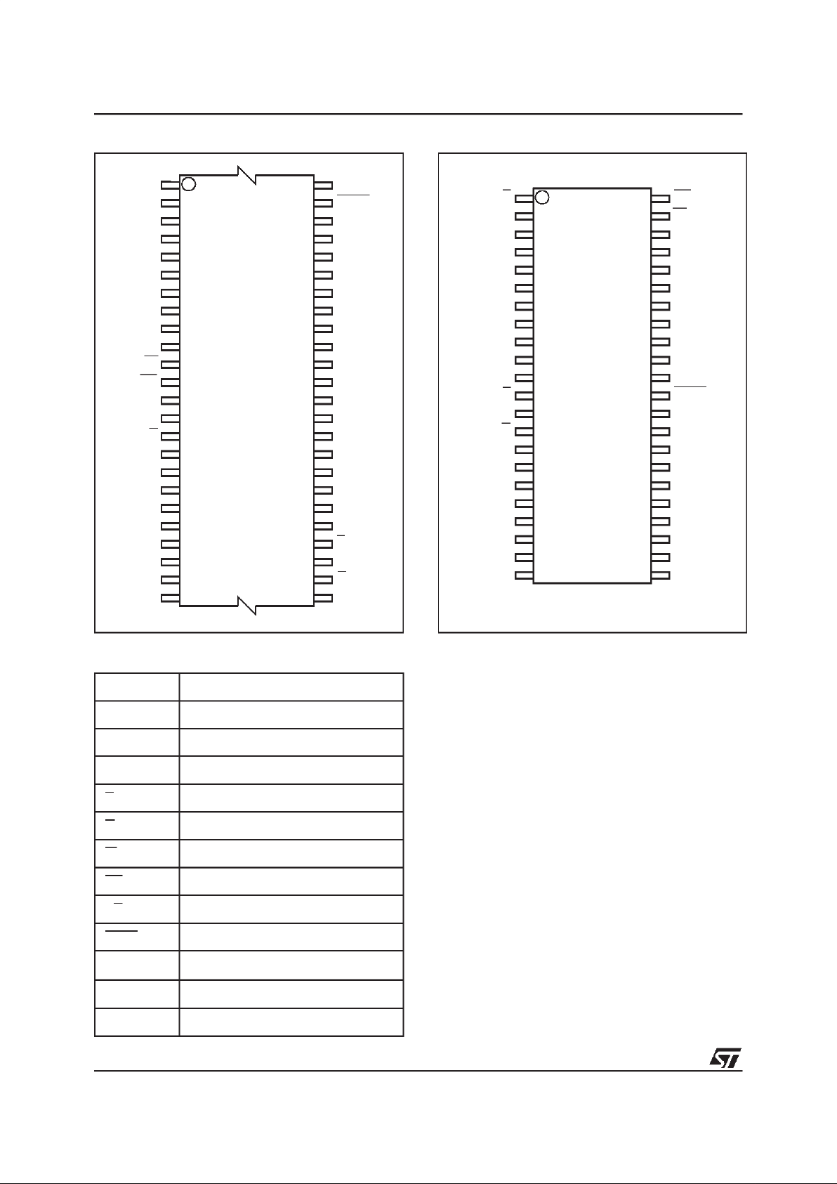
Figure 2A. TSOP Connections
DQ3
DQ9
DQ2
DQ0
DQ6
DQ13
DQ14
DQ12
DQ10
DQ15A–1
V
CC
DQ4
DQ5
DQ7
AI02199
M29F800AT
M29F800AB
12
1
13
24 25
36
37
48
DQ8
DQ1
DQ11
A16
BYTE
V
SS
A0
V
SS
A6
A3
A8
A9
A17
A10
A2
A7
NC
NC
NC
NC
A1
A18
A4
A5
A12
A13
A11
A15
A14
RP
W
RB
G
E
Table 1. Signal Names
A0-A18 Address Inputs
DQ0-DQ7 Data Inputs/Outputs
DQ8-DQ14 Data Inputs/Outputs
DQ15A–1 Data Input/Output or Address Input
E Chip Enable
G Output Enable
W Write Enable
RP Reset/Block Temporary Unprotect
RB Ready/Busy Output
BYTE Byte/Word Organization Select
V
CC
Supply Voltage
V
SS
Ground
NC Not Connected Internally
SUMMARY DESCRIPTION
The M29F800A is an 8 Mbit (1Mb x8 or 512Kb
x16) non-volatile memorythat canbe read,erased
and reprogrammed. These operations can be performed using a single 5V supply.On power-up the
memory defaultsto its Readmode where it can be
read in the same way as a ROM or EPROM.
The memory is divided into blocks that can be
erased independently so it is possible to preserve
valid data while olddata is erased. Each block can
be protected independently to prevent accidental
Program or Erase commands from modifying the
memory. Program and Erase commands arewritten to the Command Interface of the memory. An
on-chip Program/Erase Controller simplifies the
process of programming or erasingthe memoryby
taking care of all of the specialoperations that are
required to update the memory contents. The end
of a program or erase operation can be detected
and any error conditions identified. The command
set required to control the memory is consistent
with JEDEC standards.
Figure 2B. SO Connections
G
DQ0
DQ8
A3
A0
E
V
SS
A2
A1
A13
V
SS
A14
A15
DQ7
A12
A16
BYTE
DQ15A–1
DQ5DQ2
DQ3
V
CC
DQ11
DQ4
DQ14
A9
W
RB
A4
A18
RP
A7
AI02101B
M29F800AT
M29F800AB
8
2
3
4
5
6
7
9
10
11
12
13
14
15
16
32
31
30
29
28
27
26
25
24
2322
20
19
18
17DQ1
DQ9
A6
A5
DQ6
DQ13
44
39
38
37
36
35
34
33
A11
A10
DQ10
21
DQ12
40
43
1
42
41
A17 A8
3/21
M29F800AT, M29F800AB
The blocks in the memory are asymmetrically arranged, see Tables 3A and 3B, Block Addresses.
The first or last 64 Kbytes have been divided into
four additional blocks. The 16 Kbyte Boot Block
can beused forsmall initialization codeto startthe
microprocessor, the two 8 Kbyte Parameter
Blocks can be used for parameter storage and the
remaining 32K is a small MainBlock wherethe application may be stored.
Chip Enable, OutputEnable andWrite Enable signals control the bus operation of the memory.
They allow simple connection to most microprocessors, often without additional logic.
The memory is offered in TSOP48 (12 x 20mm)
and SO44 packages. Access times of 70ns and
90ns are available. The memory is supplied with
all the bits erased (set to ’1’).
SIGNAL DESCRIPTIONS
See Figure 1, Logic Diagram, and Table 1, Signal
Names, for a brief overview of thesignals connected to this device.
Address Inputs (A0-A18). The Address Inputs
select the cells in the memory array to access during Bus Read operations. During BusWrite operations they control the commands sent to the
Command Interface of the internal state machine.
Data Inputs/Outputs (DQ0-DQ7). The Data Inputs/Outputs output thedata stored at theselected
address during a Bus Readoperation. During Bus
Write operations they represent the commands
sentto theCommand Interface ofthe internal state
machine.
Data Inputs/Outputs (DQ8-DQ14). The Data Inputs/Outputs output thedata stored at theselected
address during a Bus Readoperation when BYTE
is High, VIH. When BYTE is Low, VIL, these pins
are not usedand are high impedance.During Bus
Write operations the Command Register does not
use these bits. When reading the Status Register
these bits should be ignored.
Data Input/Output or Address Input (DQ15A-1).
When BYTE is High, VIH, this pin behaves as a
Data Input/Output pin (as DQ8-DQ14). When
BYTE is Low, VIL, this pin behaves as an address
pin; DQ15A–1Low will select the LSB of theWord
on the other addresses, DQ15A–1 High will select
the MSB. Throughout the text consider references
to the Data Input/Output to include this pin when
BYTE is High and references to the Address Inputs to include this pin when BYTE is Low except
when stated explicitly otherwise.
Table 2. Absolute Maximum Ratings
(1)
Note: 1. Except for the rating ”Operating Temperature Range”, stresses above those listed in the Table ”Absolute Maximum Ratings” may
cause permanent damage to the device. These are stress ratings only and operation of the device atthese or any other conditions
above those indicated in the Operating sections of this specification is not implied. Exposure to Absolute Maximum Rating conditions forextended periods may affect device reliability. Refer also tothe STMicroelectronics SURE Program and other relevantquality documents.
2. Minimum Voltage may undershoot to –2V during transition and for less than 20ns during transitions.
Symbol Parameter Value Unit
T
A
Ambient Operating Temperature (Temperature Range Option 1) 0 to 70 °C
Ambient Operating Temperature (Temperature Range Option 6) –40 to 85 °C
Ambient Operating Temperature (Temperature Range Option 3) –40 to 125 °C
T
BIAS
Temperature Under Bias –50 to 125 °C
T
STG
Storage Temperature –65 to 150 °C
V
IO
(2)
Input or Output Voltage –0.6 to 6 V
V
CC
Supply Voltage –0.6 to 6 V
V
ID
Identification Voltage –0.6 to 13.5 V
M29F800AT, M29F800AB
4/21
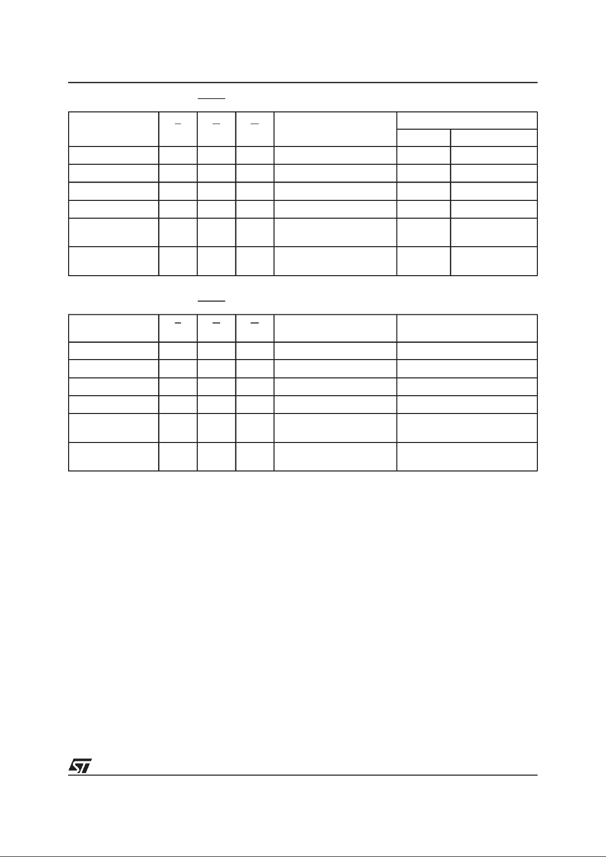
Table 3A. M29F800AT Block Addresses
Size
(Kbytes)
Address Range
(x8)
Address Range
(x16)
16 FC000h-FFFFFh 7E000h-7FFFFh
8 FA000h-FBFFFh 7D000h-7DFFFh
8 F8000h-F9FFFh 7C000h-7CFFFh
32 F0000h-F7FFFh 78000h-7BFFFh
64 E0000h-EFFFFh 70000h-77FFFh
64 D0000h-DFFFFh 68000h-6FFFFh
64 C0000h-CFFFFh 60000h-67FFFh
64 B0000h-BFFFFh 58000h-5FFFFh
64 A0000h-AFFFFh 50000h-57FFFh
64 90000h-9FFFFh 48000h-4FFFFh
64 80000h-8FFFFh 40000h-47FFFh
64 70000h-7FFFFh 38000h-3FFFFh
64 60000h-6FFFFh 30000h-37FFFh
64 50000h-5FFFFh 28000h-2FFFFh
64 40000h-4FFFFh 20000h-27FFFh
64 30000h-3FFFFh 18000h-1FFFFh
64 20000h-2FFFFh 10000h-17FFFh
64 10000h-1FFFFh 08000h-0FFFFh
64 00000h-0FFFFh 00000h-07FFFh
Table 3B. M29F800AB Block Addresses
Size
(Kbytes)
Address Range
(x8)
Address Range
(x16)
64 F0000h-FFFFFh 78000h-7FFFFh
64 E0000h-EFFFFh 70000h-77FFFh
64 D0000h-DFFFFh 68000h-6FFFFh
64 C0000h-CFFFFh 60000h-67FFFh
64 B0000h-BFFFFh 58000h-5FFFFh
64 A0000h-AFFFFh 50000h-57FFFh
64 90000h-9FFFFh 48000h-4FFFFh
64 80000h-8FFFFh 40000h-47FFFh
64 70000h-7FFFFh 38000h-3FFFFh
64 60000h-6FFFFh 30000h-37FFFh
64 50000h-5FFFFh 28000h-2FFFFh
64 40000h-4FFFFh 20000h-27FFFh
64 30000h-3FFFFh 18000h-1FFFFh
64 20000h-2FFFFh 10000h-17FFFh
64 10000h-1FFFFh 08000h-0FFFFh
32 08000h-0FFFFh 04000h-07FFFh
8 06000h-07FFFh 03000h-03FFFh
8 04000h-05FFFh 02000h-02FFFh
16 00000h-03FFFh 00000h-01FFFh
Chip Enable (E). The Chip Enable, E, activates
the memory,allowing BusRead and Bus Writeoperations to be performed. When Chip Enable is
High, VIH, all other pins are ignored.
Output Enable (G). The Output Enable, G, controls the Bus Read operation of the memory.
Write Enable (W). The WriteEnable, W, controls
the Bus Write operation of the memory’s Command Interface.
Reset/BlockTemporaryUnprotect(RP). The Reset/Block Temporary Unprotect pin can be used to
apply a Hardware Reset to the memory or totemporarily unprotect all blocks that have been protected.
A Hardware Reset is achieved by holding Reset/
Block Temporary Unprotect Low, VIL, for at least
t
PLPX
. After Reset/Block Temporary Unprotect
goes High, VIH, the memory will be ready for Bus
Read and Bus Write operations after t
PHEL
or
t
RHEL
, whicheveroccurs last. See the Ready/Busy
Output section, Table 14 and Figure 10, Reset/
Temporary Unprotect AC Characteristics for more
details.
Holding RP at VIDwill temporarily unprotect the
protected blocks in the memory. Program and
Erase operations on all blocks will be possible.
The transition fromVIHtoVIDmustbe slower than
t
PHPHH
.
Ready/Busy Output (RB). The Ready/Busy pin
is anopen-drain output that can beused to identify
when the memory array can be read. Ready/Busy
is high-impedance during Read mode,Auto Select
mode and Erase Suspend mode.
After a Hardware Reset, Bus Read and Bus Write
operations cannot begin until Ready/Busy becomes high-impedance. See Table 14 and Figure
10, Reset/Temporary Unprotect AC Characteristics.
During Program or Erase operations Ready/Busy
is Low, VOL. Ready/Busy will remain Low during
Read/Reset commands or Hardware Resets until
the memory is ready to enter Read mode.
The use ofan open-drain output allowsthe Ready/
Busy pins fromseveral memories tobe connected
to asingle pull-up resistor. A Low will then indicate
that one, or more, of the memories is busy.
Byte/WordOrganizationSelect(BYTE). The Byte/
Word OrganizationSelect pinis used to switch between the 8-bitand 16-bit Bus modes of the memory. When Byte/Word Organization Select is Low,
VIL, the memory is in 8-bit mode, when it is High,
VIH, the memory is in 16-bit mode.
5/21
M29F800AT, M29F800AB
Table 4A. Bus Operations, BYTE = V
IL
Note: X = VILor VIH.
Table 4B. Bus Operations, BYTE = V
IH
Note: X = VILor VIH.
Operation E G W
Address Inputs
DQ15A–1, A0-A18
Data Inputs/Outputs
DQ14-DQ8 DQ7-DQ0
Bus Read V
IL
V
IL
V
IH
Cell Address Hi-Z Data Output
Bus Write
V
IL
V
IH
V
IL
Command Address Hi-Z Data Input
Output Disable X
V
IH
V
IH
X Hi-Z Hi-Z
Standby
V
IH
X X X Hi-Z Hi-Z
Read Manufacturer
Code
V
IL
V
IL
V
IH
A0 = VIL,A1=VIL,A9=VID,
Others V
IL
or V
IH
Hi-Z 20h
Read Device Code
V
IL
V
IL
V
IH
A0 = VIH,A1=VIL,A9=VID,
Others V
IL
or V
IH
Hi-Z
ECh (M29F800AT)
58h (M29F800AB)
Operation E G W
Address Inputs
A0-A18
Data Inputs/Outputs
DQ15A–1, DQ14-DQ0
Bus Read
V
IL
V
IL
V
IH
Cell Address Data Output
Bus Write
V
IL
V
IH
V
IL
Command Address Data Input
Output Disable X
V
IH
V
IH
X Hi-Z
Standby
V
IH
X X X Hi-Z
Read Manufacturer
Code
V
IL
V
IL
V
IH
A0 = VIL,A1=VIL,A9=VID,
Others V
IL
or V
IH
0020h
Read Device Code
V
IL
V
IL
V
IH
A0 = VIH,A1=VIL,A9=VID,
Others V
IL
or V
IH
00ECh (M29F800AT)
0058h (M29F800AB)
VCCSupply Voltage. The VCCSupply Voltage
supplies the power for all operations (Read, Program, Erase etc.).
The Command Interface is disabled whenthe V
CC
Supply Voltage is less than the Lockout Voltage,
V
LKO
. Thisprevents BusWrite operationsfrom accidentally damaging the data during power up,
power down and power surges. If the Program/
Erase Controller is programming or erasingduring
this time then the operation aborts and the memory contents being altered will be invalid.
A 0.1µF capacitor should be connected between
the VCCSupply Voltage pin and the VSSGround
pin to decouple the current surges from the power
supply. The PCB trackwidths must be sufficient to
carry the currents required during program and
erase operations, I
CC4
.
VSSGround. TheVSSGroundis the reference for
all voltage measurements.
BUS OPERATIONS
There are five standard bus operations that control
the device. These are Bus Read, Bus Write, Output Disable,Standby and Automatic Standby. See
Tables 4A and 4B, Bus Operations, for a summary. Typically glitches of less than 5ns on Chip Enable or Write Enable are ignored by the memory
and do not affect bus operations.
Bus Read. Bus Read operations read from the
memory cells, or specific registers in the Command Interface. A valid Bus Read operation involves settingthe desired address on the Address
Inputs, applying a Low signal, VIL, to Chip Enable
and Output Enable and keeping Write Enable
High, VIH. The Data Inputs/Outputs will outputthe
value, see Figure 7, Read Mode AC Waveforms,
and Table11, Read ACCharacteristics, for details
of when the output becomes valid.
Bus Write. Bus Write operations write to the
Command Interface. A valid Bus Write operation
begins by setting the desired address on the Ad-

M29F800AT, M29F800AB
6/21
dress Inputs. The Address Inputs are latched by
the CommandInterface on the falling edgeof Chip
Enable or Write Enable, whichever occurs last.
The Data Inputs/Outputs are latched by theCommand Interface on the rising edge of Chip Enable
or WriteEnable, whichever occursfirst.Output Enable must remain High, VIH, during the whole Bus
Write operation. See Figures 8 and 9, Write AC
Waveforms, and Tables 12 and 13, Write AC
Characteristics, for details of the timing requirements.
Output Disable. The Data Inputs/Outputs are in
the high impedance state when Output Enable is
High, VIH.
Standby. When Chip Enable is High, VIH, the
Data Inputs/Outputs pins are placed in the highimpedance state and the Supply Current is reduced to the Standby level.
When Chip Enable is at VIHthe Supply Current is
reduced to the TTL Standby Supply Current,I
CC2
.
To furtherreduce the SupplyCurrent tothe CMOS
Standby Supply Current, I
CC3
, ChipEnable should
be held within VCC± 0.2V. For Standby current
levels see Table 10, DC Characteristics.
During program or erase operations the memory
will continue to use the Program/Erase Supply
Current, I
CC4
, forProgram or Erase operationsun-
til the operation completes.
AutomaticStandby. If CMOS levels (VCC± 0.2V)
are usedto drive thebus and the busis inactivefor
150ns or more the memory enters Automatic
Standby where the internal Supply Current is reduced tothe CMOS Standby Supply Current,I
CC3
.
The Data Inputs/Outputs will still output data if a
Bus Read operation is in progress.
Special Bus Operations
Additional bus operations can be performed to
read the Electronic Signature and also to apply
and remove Block Protection. These bus operations are intended for use by programming equipment and are not usually used in applications.
They require VIDto be applied to some pins.
Electronic Signature. The memory has two
codes, the manufacturer code and the device
code, that can be read to identify the memory.
These codes can be read by applying the signals
listed in Tables 4A and 4B, Bus Operations.
Block Protection andBlocksUnprotection. Each
block can be separately protected against accidental Program or Erase.Protected blocks can be
unprotected to allow data to be changed. Block
Protection and Block Unprotection operations
must only be performed on programming equipment.
For further information refer to Application Note
AN1122, Applying Protection and Unprotection to
M29 Series Flash.
COMMAND INTERFACE
All Bus Write operations to the memory are interpreted by the Command Interface. Commands
consist of one or more sequential Bus Write operations. Failure toobserve a valid sequence of Bus
Write operations will result in the memory returning toRead mode. In this case, after at least 50ns,
an address transition or Chip Enable going Low is
required before reading correct data. The long
command sequences are imposed to maximize
data security.
The address used for the commands changes depending on whether the memory is in 16-bit or 8bit mode. See either Table 5A, or 5B, depending
on the configuration that is being used, for a summary of the commands.
Read/Reset Command. The Read/Reset command returns the memory toits Read mode where
it behaves like a ROM or EPROM. It also resets
the errors in the Status Register. Either one or
three Bus Write operations can be used to issue
the Read/Reset command.
If the Read/Reset command is issued during a
Block Erase operation orfollowing a Programming
or Erase errorthen the memory willtakeup to10µs
to abort. During the abort period no validdata can
be read from the memory. Issuing a Read/Reset
command during a Block Erase operation will
leave invalid data in the memory.
Auto Select Command. The Auto Select command is used to read the Manufacturer Code, the
Device Code and the Block Protection Status.
Three consecutive Bus Write operations are required to issue the Auto Select command. Once
the Auto Select command is issued the memory
remains in Auto Select mode until another command is issued.
From the Auto Select mode the Manufacturer
Code can be read using a Bus Read operation
with A0 = VILandA1 = VIL. The otheraddress bits
may be set to either VILor VIH. The Manufacturer
Code for STMicroelectronics is 0020h.
The Device Code can be read using a Bus Read
operation with A0 = VIHand A1 = VIL. The other
address bits may be set to either VILor VIH. The
Device Codefor theM29F800AT is 00ECh and for
the M29F800AB is 0058h.
The Block Protection Status of each block can be
read using a Bus Read operation with A0 = VIL,
A1 = VIH, and A12-A18 specifying the address of
the block. The otheraddress bitsmay be set to either VILor VIH. If the addressed block is protected
then 01h is output on Data Inputs/Outputs DQ0DQ7, otherwise 00h is output.
Program Command. The Program command
can be used to program a value to one address in
the memory array at a time. The command re-
7/21
M29F800AT, M29F800AB
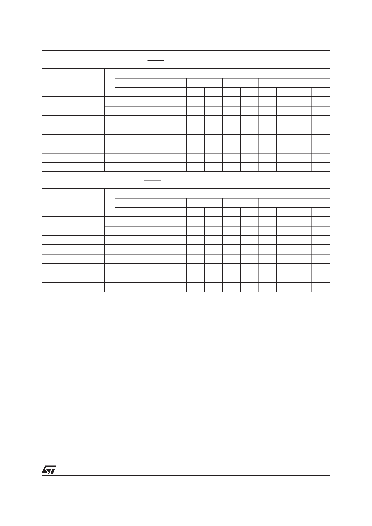
Table 5A. Commands, 16-bit mode, BYTE = V
IH
Table 5B. Commands, 8-bit mode, BYTE = V
IL
Note: X Don’t Care, PA Program Address, PD Program Data, BA Any address in the Block.
All values in the table are in hexadecimal.
The Command Interface only uses A–1, A0-A10 and DQ0-DQ7 to verify the commands; A11-A18, DQ8-DQ14 and DQ15 are Don’t Care.
DQ15A–1 is A–1 when BYTE is V
IL
or DQ15 when BYTE is VIH.
Read/Reset. After a Read/Reset command, read the memory as normal until another command is issued.
Auto Select. After an Auto Select command, readManufacturer ID, Device ID or Block Protection Status.
Program, Chip Erase, Block Erase. After these commands read the Status Register until the Program/Erase Controller completes and the
memory returns to Read Mode. Add additional Blocks during Block Erase Command withadditional Bus Write Operations until the Timeout
Bit is set.
Erase Suspend. After the EraseSuspend command readnon-erasing memory blocks as normal, issue AutoSelect and Program commands
on non-erasing blocks as normal.
Erase Resume. After the Erase Resume command the suspended Erase operation resumes, read the Status Register until the Program/
Erase Controller completes and the memory returns to Read Mode.
Command
Length
Bus Write Operations
1st 2nd 3rd 4th 5th 6th
Addr Data Addr Data Addr Data Addr Data Addr Data Addr Data
Read/Reset
1X F0
3 555 AA 2AA 55 X F0
Auto Select 3 555 AA 2AA 55 555 90
Program 4 555 AA 2AA 55 555 A0 PA PD
Chip Erase 6 555 AA 2AA 55 555 80 555 AA 2AA 55 555 10
Block Erase 6+ 555 AA 2AA 55 555 80 555 AA 2AA 55 BA 30
Erase Suspend 1 X B0
Erase Resume 1 X 30
Command
Length
Bus Write Operations
1st 2nd 3rd 4th 5th 6th
Addr Data Addr Data Addr Data Addr Data Addr Data Addr Data
Read/Reset
1X F0
3 AAA AA 555 55 X F0
Auto Select 3 AAA AA 555 55 AAA 90
Program 4 AAA AA 555 55 AAA A0 PA PD
Chip Erase 6 AAA AA 555 55 AAA 80 AAA AA 555 55 AAA 10
Block Erase 6+ AAA AA 555 55 AAA 80 AAA AA 555 55 BA 30
Erase Suspend 1 X B0
Erase Resume 1 X 30
quires fourBus Write operations,the final write operation latchesthe address and data inthe internal
state machine and starts the Program/Erase Controller.
If the address falls in a protected block then the
Program command is ignored, the data remains
unchanged. The Status Registeris neverread and
no error condition is given.
During the program operation the memory will ignore all commands. It is not possible to issue any
command to abort orpause theoperation. Typical
program times are given inTable 6. Bus Read operations during the program operation will output
the Status Register on the Data Inputs/Outputs.
See the section on the Status Register for more
details.
After the program operation has completed the
memory will return to the Read mode, unless an
error has occurred. When an error occurs the
memory will continue to output the Status Register. A Read/Reset command must be issued to reset the error condition and return to Read mode.
Note thatthe Program command cannotchange a
bit set at ’0’ backto ’1’ and attempting to do so will
cause anerror. One of the Erase Commands must
be used to set all thebits in a blockor in the whole
memory from ’0’ to ’1’.
 Loading...