

512 Kbit (64Kb x8, Bulk) Single Supply Flash Memory
■ SINGLE 5V±10% SUPPL Y VOLTAGE for
PROGRAM, ERAS E and READ O PER AT IONS
■ ACCESS TIME: 45ns
■ PROGRAMMING TIME
– 8µs per Byte typical
■ PROGRAM/E RA SE CONTROLLER
– Embedded Byte Program algorithm
– Embedded Chip Erase algorithm
– Status Register Polling and Toggle Bits
■ UNLOCK BYPASS PROGRAM COMMAND
– Faster Production/Batch Programming
■ LOW POWER CONSUMPTION
– Standby and Automatic Standby
■ 100,000 PROGRAM/ERASE CYCL ES
■ 20 YEARS DATA RETENTI ON
– Defectivity below 1 ppm/year
■ ELECTRONIC SIGNATURE
– Manufacturer Code: 20h
– Device Code: 24h
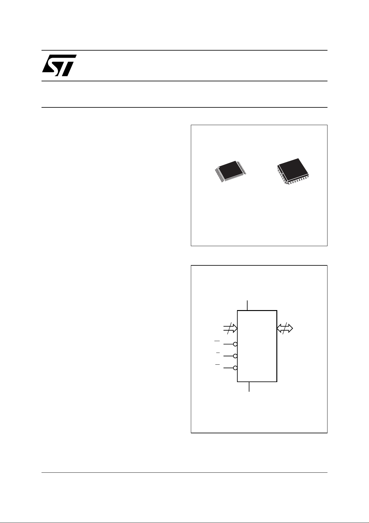
TSOP32 (NZ)
8 x 14mm
Figure 1. Logic Diagram
V
CC
M29F512B
PRELIMINARY DATA
PLCC32 (K)
16
A0-A15
W
E
G
July 1999
This is preliminary information on a new product now in development or undergoing evaluation. Details are subject to change without notice.
M29F512B
V
SS
8
DQ0-DQ7
AI02739
1/16
M29F512B
Figure 2A. TSOPConnections
A11 G
A9
A8
A13
A14
NC
V
CC
NC
NC
A15
A12
A7
A6
A5
A4 A3
1
W
8
M29F512B
9
16 17
32
25
24
AI02741
A10
E
DQ7
DQ6
DQ5
DQ4
DQ3
V
SS
DQ2
DQ1
DQ0
A0
A1
A2
Figure 2B. PLCC Connections
CC
NC
A7
A6
A5
A4
A3
A2
A1
A0
DQ0
A12
9
DQ1
NC
A15
32
1
M29F512B
17
SS
V
DQ2
DQ3
V
DQ4
W
DQ5
NC
25
DQ6
A14
A13
A8
A9
A11
G
A10
E
DQ7
AI02930
Table 1. Signal Names
A0-A15 Address Inputs
DQ0-DQ7 Data Inputs/Outputs
E
G
W
V
CC
V
SS
NC Not Connected Internally
Chip Enable
Output Enable
Write Enable
Supply Voltage
Ground
SUMMARY DESCRIPTION
The M29F512B is a 512 Kbit (64Kb x 8) non-volatile memory that can be read, erased and reprogrammed. These operations can be performed
using a single 5V supply. On power-up the memory defaults to its Read m ode where it can be read
in the same way as a ROM or EPROM.
Program and Erase command s are written to the
Command Interface of the memory. An on-chip
Program/Erase Controller simplifies the process of
programming or erasing the memory by taking
care of all of the special operations that are re-
quired to update the memory contents. The end of
a program or erase operation can be detected and
any error conditions identified. The command set
required to control the memory is consistent with
JEDEC standards.
Chip Enable, Output Enable and Write Enable signals control the bus operation of the memory.
They allow simple conne ction to most m icroprocessors, often without additional logic.
The memory is offered in TSOP32 (8 x 14mm) and
PLCC32 packages. Access times of 45ns and
70ns are available. The m emory is supplied with
all the bits erased (set to ’1’).
SIGNAL DESCRIPTIONS
See Figure 1, Logic Diagram, and Table 1, Sig nal
Names, for a brief overview of the signals connected to this device.
Address Inputs (A0-A15). The Address Inputs
select the cells i n the memory array to a ccess during Bus Read operations. During Bus Write operations they control the commands sent to the
Command Interface of the internal state machine.
Data Inputs/Outputs (DQ0-DQ7). The Data Inputs/Outputs output the data stored at the selected
address during a Bus Read operation. During Bus
Write operations they represent the commands
sent to the Command Interface of the internal state
machine.
2/16

M29F512B
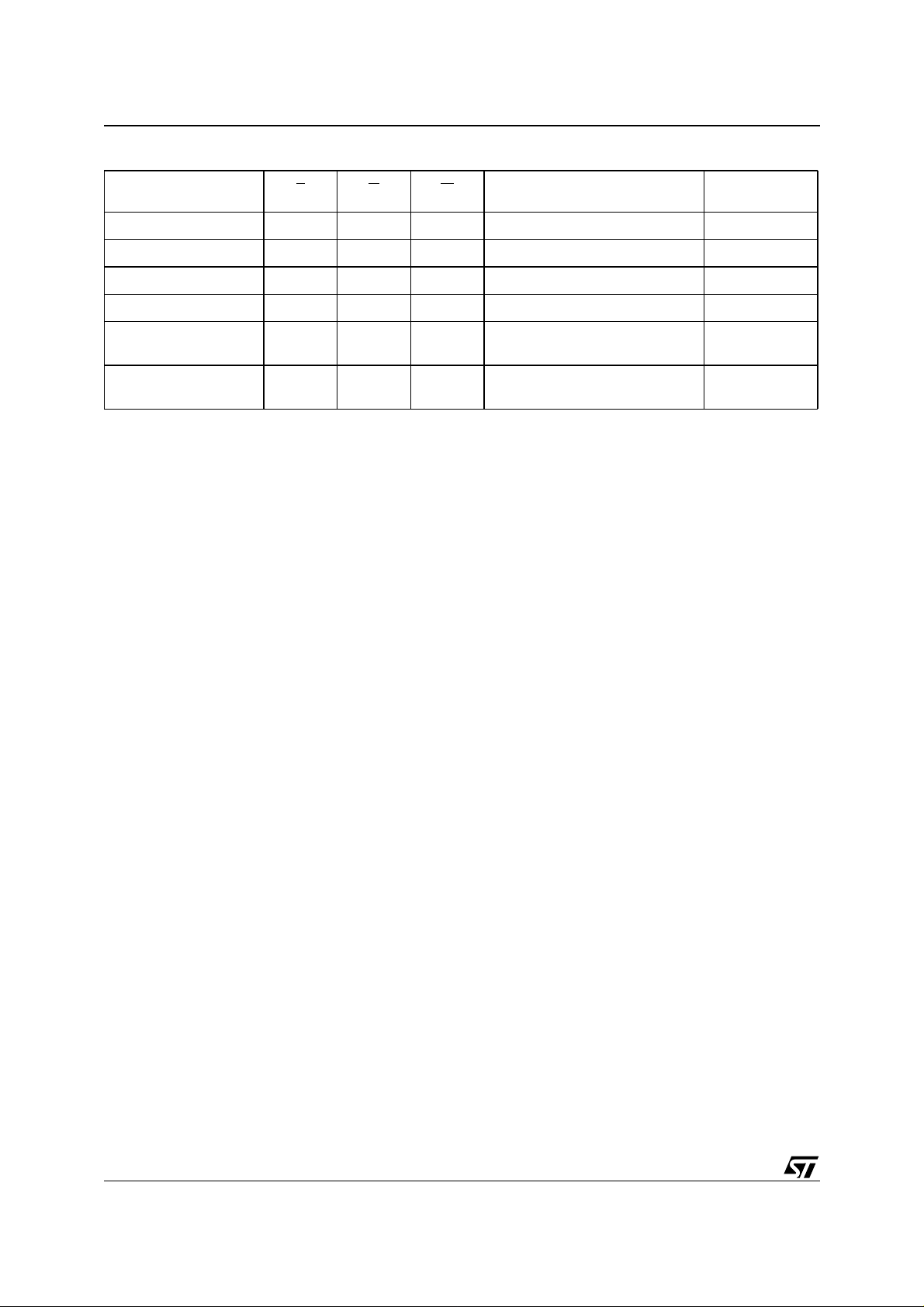
Table 2. Absolute Maximum Ratings
Symbol Parameter Value Unit
T
A
T
BIAS
T
STG
(2)
V
IO
V
CC
V
ID
Note: 1. Except for the rating "Operating Temperature Range", stresses above those listed in the Table "Absolute Maximum Ratings" may
cause permanent damage to the device. These are stress ratings only and operation of the device at these or any other conditions
above those indicated in the Operating section s of this specific at i on is not impli ed. Exposure to Absolu te Maximum Rati ng conditions for extended periods may affect device reliability. Refer also to the STMicroelectronics SURE Program and other relevant
quality documents.
2. Mini m um Voltage may undershoot to –2V duri ng transit i on and for less than 20ns duri ng transitio ns.
Ambient Operating Temperature 0 to 70 °C
Temperature Under Bias –50 to 125 °C
Storage Temperature –65 to 150 °C
Input or Output Voltage –0.6 to 6 V
Supply Voltage –0.6 to 6 V
Identification Voltage –0.6 to 13.5 V
Chip Enable (E). The Chip Enable, E, activates
the memory, allowing Bus Read and Bus Write operations to be performed. When Chip Enable is
High, V
Output Enable (G
, all other pins are ignored.
IH
). The Output Enable, G, con-
trols the Bus Read operation of the memory.
Write Enable (W
). The Write Enable, W, controls
the Bus Write operation of the memory’s Command Interf a c e .
Supply Voltage. The VCC Supply Voltage
V
CC
supplies the power for all operations (Read, Program, Erase etc.).
The Command Interface is disabled when the V
Supply Voltage is less than the L ockout Voltage,
V
. This prevents Bus Write operations from ac-
LKO
cidentally damaging the data during power up,
power down and power surges. If the Program/
Erase Controller is programming or erasing during
this time then the operation aborts and the memory contents being altered will be invalid.
A 0.1µF capacitor should be connected between
the V
Supply Voltage pin and the VSS Ground
CC
pin to decouple the current surges from the power
supply. The PCB track widths must be sufficient to
carry the currents required during program and
erase operations, I
Vss Ground. The V
.
CC3
Ground is the reference
SS
for all voltage measurements.
(1)
CC
BUS OPERATIONS
There are five standard bus operations that control
the device. These are Bus Read, Bus Wri te, Output Disable, Standby and Automatic Standby. See
Table 3, Bus Operations, for a summary. Typically
glitches of less than 5ns are ig nored b y the mem ory and do not affect bus operations.
Bus Read. Bus Read operations read from the
memory cells, or specific registers in the Command Interface. A valid Bus Read operation involves setting the desired address on the Address
Inputs, applying a Low sig nal, V
, to Chip Enable
IL
and Output Enable and keeping Write Enable
High, V
. The Data Inputs/Outputs will output the
IH
value, see Figure 7, Rea d Mode AC Wav eforms,
and Table 10, Read AC Characteristics, for details
of when the output becomes valid.
Bus Write. Bus Write operations write to the
Command Interface. A valid Bus Write operation
begins by setting the des ired address on t he Address Inputs. The Address Inputs are latched by
the Command Interface on the falling edge of Chip
Enable or Write Enable, whichever occurs last.
The Data Inputs/Outputs a re latched by the Command Interface on the rising edge of Chip Enable
or Write Enable, whichever occurs first. Output Enable must remain High, V
, during the whole Bus
IH
Write operation. See Figures 8 an d 9, Write AC
Waveforms, and Tables 11 and 12, Write AC
Characteristics, for details of the timing requirements.
3/16
M29F512B
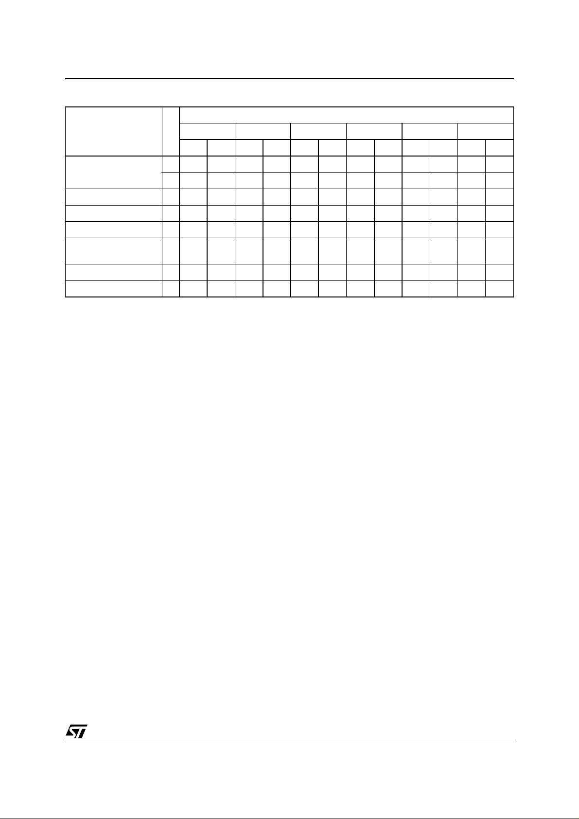
Table 3. Bus Operations
Operation E G W Address Inputs
Bus Read
Bus Write
Output Disable X
Standby
Read Manufacturer
Code
Read Device Code
Note: X = VIL or VIH.
Data
Inputs/Outputs
V
IL
V
IL
V
IH
V
IL
V
IL
V
IL
V
IH
V
IH
XXX Hi-Z
V
IL
V
IL
V
V
V
V
V
Cell Address Data Output
IH
Command Address Data Input
IL
XHi-Z
IH
A0 = VIL, A1 = VIL, A9 = VID,
IH
Others V
A0 = VIH, A1 = VIL, A9 = VID,
IH
Others V
IL
IL
or V
or V
IH
IH
20h
24h
Output Disa bl e . The Data Inputs/Outputs are in
the high impedance s tate when Output Enable is
High, V
Standby. When Chip Enable is High, V
.
IH
, the
IH
memory enters Standby mode and the Data Inputs/Outputs pins are placed in the high-impedance state. To reduce the S upply Current to the
Standby Supply Current, I
be held within V
± 0.2V. For the Standby current
CC
, Chip Enable should
CC2
level see Table 9, DC Characteristics.
During program or erase operations the memory
will continue to use the Program/Erase Supply
Current, I
, for Program or Erase operations un-
CC3
til the operation completes.
Automatic Standby. If CMOS levels (V
± 0.2V)
CC
are used to drive the bus and the bus is inactive for
150ns or more the memory enters Automatic
Standby where the internal Supply Current is reduced to the Standby Supply Current, I
CC2
. The
Data Inputs/Outputs will still output data if a Bus
Read operation is in progress.
Special Bus Operations
Additional bus operations can be performed to
read the Electronic S ignature. These bus operations are intended for use by programming equipment and are not usually used in applications.
They require V
to be applied to some pins.
ID
Electronic Signature. The memory has two
codes, the manufacturer code and the device
code, that can be read to identify the memory.
These codes can be read by applying t he signals
listed in Table 3, Bus Operations.
COMMAND INTERFACE
All Bus Write operations t o the me mory are in terpreted by the Command Interface. Commands
consist of one or more sequential Bus Write operations. Failure to observe a valid sequence of Bus
Write operations will result in the memory returning to Read mode. The long command sequences
are imposed to maximize data security.
The commands are summarized in Table 4, Commands. Refer to Table 4 in conjunction with the
text descriptions below.
Read/Reset Command. The Read/Reset command returns the memory to its Read mode where
it behaves like a ROM or EPROM. It also resets
the errors in the Status Register. Either one or
three Bus Write operations can be u sed to issue
the Read/Reset command.
If the Read/Reset command is issued during a
Chip Erase operation the memory will take about
10µs to abort the Chip Erase. During the abort period no valid data can be read from the memory.
Issuing a Read/Reset command during a Chip
Erase operation will leave invalid data in the memory.
Auto Select Command. The Auto Select command is used to read the Manufacturer Code and
the Device Code. Three consecutive Bus Write operations are required to issue the Auto Select command. Once the Auto Select command is issued
the memory remains in Auto Select mode until another command is issued.
4/16
M29F512B
Table 4. Commands
Bus Write Operations
Command
Read/Reset
Auto Select 3 555 AA 2AA 55 555 90
Program 4 555 AA 2AA 55 555 A0 PA PD
Unlock Bypass 3 555 AA 2AA 55 555 20
Unlock Bypass
Program
Unlock Bypass Reset 2 X 90 X 00
Chip Erase 6 555 AA 2AA 55 555 80 555 AA 2AA 55 555 10
Note: X Don’t Care, PA Program Address, PD Program Data.
All values in the table are in hexadecimal.
The Comman d Interface only uses add ress bits A0-A 10 to verify the comman ds, the upper address bits are Don’t Care.
Read/Re set. After a Read/Reset command, read the memory as normal until another command is issued.
Auto Select. After an Auto Select command, read Manufacturer ID or Device ID.
Program, Un lock Bypa ss Program, Ch ip Erase. After t hese commands read the Sta tus Registe r until the Program/Eras e Controlle r com-
pletes and the memory re turns to Re ad M ode.
Unlock Bypass. After the Unlock Bypass command issue Unlock Bypass Program or Unlock Bypass Reset commands.
Unlock Bypass Reset. After the Unlock Bypass Reset command read the memory as normal until another command is issued.
1X F0
3 555 AA 2AA 55 X F0
2X A0PAPD
1st 2nd 3rd 4th 5th 6th
Length
Addr Data Addr Data Addr Data Addr Data Addr Data Addr Data
From the Auto Select mode the Manufacturer
Code can be read using a Bus Read operation
with A0 = V
may be set to either V
and A1 = VIL. The other address bits
IL
or VIH. The Manufa cturer
IL
Code for STMicroelectronics is 20h.
The Device Code can be read using a B us Read
operation with A0 = V
address bits may be set to e ither V
and A1 = VIL. The other
IH
or VIH. The
IL
Device Code for the M29F512B is 24h.
Program Command. The Program command
can be used to program a value to one address in
the memory array at a time. The command requires four Bus Write operations, the final write operation latches the address and data in the internal
state machine and starts the Program/Erase Controller.
During the program operat ion the memo ry will ignore all commands. I t is n ot poss ible t o iss ue any
command to abort or pause the operation. Typical
program times are given in Table 5. Bus Read operations during the program o peration will output
the Status Register on the Data Inputs/Outputs.
See the section on the S tatus Register for more
details.
After the program operation has completed the
memory will return to the Read mode, unle ss an
error has occurred. When an error occurs the
memory will continue to output the Status Register. A Read/Reset command must be issued to reset the error condition and return to Read mode.
Note that the Program command cannot change a
bit set at ’0’ back to ’1’ and attempting to do so will
cause an error. The Chip Erase command must be
used to set all the bits in the memory from ’0’ to ’1’.
Unlock Bypass Command. The Unlock Bypass
command is used in conjunction with the Unlock
Bypass Program command to program the memory. When the access time to the device is long (as
with some EPROM programmers) considerable
time saving can be made by using these commands. Three Bus Write operations are requ ired
to issue the Unlock Bypass command.
Once the Unlock Bypas s command has bee n issued the memory will only accept the Unloc k Bypass Program command and the Unlock Bypass
Reset command. The memory can be read as if in
Read mode.
5/16
 Loading...