

SGS Thomson Microelectronics M29F400BT90N6, M29F400BT70N6, M29F400BT70N1, M29F400BT70M1, M29F400BT55N1 Datasheet
...
4 Mbit (512Kb x8 or 256Kb x16, Boot Block)
■ SINGLE 5V±10% SUPPLY VOLTAGE for
PROGRAM, ERASE and READ OPERATIONS
■ ACCESS TIME: 45ns
■ PROGRAMMING TIME
–8µs per Byte/Word typical
■ 11 MEMORY BLOCKS
– 1 Boot Block (Top or Bottom Location)
– 2 Parameter and 8 Main Blocks
■ PROGRAM/ERASE CONTROLLER
– Embedded Byte/Word Program algorithm
– Embedded Multi-Block/Chip Erase algorithm
– Status Register Polling and Toggle Bits
– Ready/Busy Output Pin
■ ERASE SUSPEND and RESUME MODES
– Read and Program another Block during
Erase Suspend
■ UNLOCK BYPASS PROGRAM COMMAND
– Faster Production/Batch Programming
■ TEMPORARY BLOCK UNPROTECTION
MODE
■ LOW POWERCONSUMPTION
– Standby and Automatic Standby
■ 100,000 PROGRAM/ERASE CYCLESper
BLOCK
■ 20 YEARS DATA RETENTION
– Defectivity below 1 ppm/year
■ ELECTRONIC SIGNATURE
– Manufacturer Code: 0020h
– M29F400BT Device Code: 00D5h
– M29F400BB Device Code: 00D6h
M29F400BT
M29F400BB
Single Supply Flash Memory
PRELIMINARY DATA
44
1
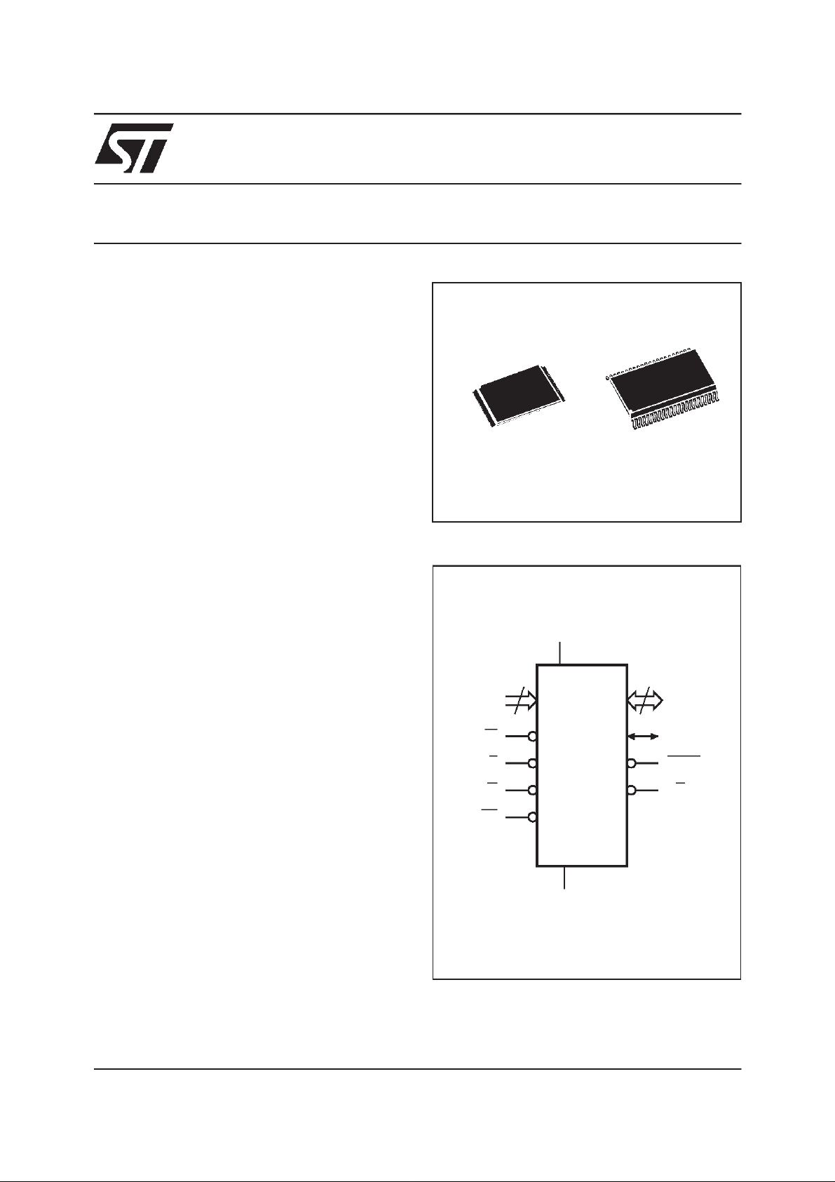
TSOP48(N)
12 x 20mm
Figure 1. Logic Diagram
V
CC
18
A0-A17
W
E
G
RP
M29F400BT
M29F400BB
V
SS
SO44 (M)
15
DQ0-DQ14
DQ15A–1
BYTE
RB
AI02904
October 1999
This is preliminary information on a new product now in development or undergoing evaluation. Details are subject to change without notice.
1/22
M29F400BT, M29F400BB
Figure 2A. TSOP Connections
A15
A14
A13
A12
A11
A10 DQ14
NC
NC
RP
NC
NC
RB
NC
A17
1
A9
A8
W
12
M29F400BT
M29F400BB
13
A7
A6
A5
A4
A3
A2
A1
24 25
48
37
36
AI02905
A16
BYTE
V
SS
DQ15A–1
DQ7
DQ6
DQ13
DQ5
DQ12
DQ4
V
CC
DQ11
DQ3
DQ10
DQ2
DQ9
DQ1
DQ8
DQ0
G
V
SS
E
A0
Figure 2B. SO Connections
NC RP
A17 A8
V
SS
DQ0
DQ8
DQ9
DQ10
DQ3
DQ11
A7
A6
A5
A4
A3
A2
A1
A0
1
2
3
4
5
6
7
8
9
10
11
M29F400BT
E
G
M29F400BB
12
13
14
15
16
17DQ1
18
19
20
21
44
43
42
41
40
39
38
37
36
35
34
33
32
31
30
29
28
27
26
25
24
2322
AI02906
WRB
A9
A10
A11
A12
A13
A14
A15
A16
BYTE
V
SS
DQ15A–1
DQ7
DQ14
DQ6
DQ13
DQ5DQ2
DQ12
DQ4
V
CC
Table 1. Signal Names
A0-A17 Address Inputs
DQ0-DQ7 Data Inputs/Outputs
DQ8-DQ14 Data Inputs/Outputs
DQ15A–1 Data Input/Output or Address Input
E Chip Enable
G Output Enable
W Write Enable
RP Reset/Block Temporary Unprotect
RB Ready/Busy Output
BYTE Byte/Word Organization Select
V
CC
V
SS
NC Not Connected Internally
2/22
Supply Voltage
Ground
SUMMARY DESCRIPTION
The M29F400B is a 4 Mbit (512Kb x8 or 256Kb
x16) non-volatile memorythat canbe read,erased
and reprogrammed. These operations can be performed using a single 5V supply.On power-up the
memory defaultsto its Readmode where it can be
read in the same way as a ROM or EPROM. The
M29F400B is fully backward compatible with the
M29F400.
The memory is divided into blocks that can be
erased independently so it is possible to preserve
valid data while olddata is erased. Each block can
be protected independently to prevent accidental
Program or Erase commands from modifying the
memory. Program and Erase commands arewritten to the Command Interface of the memory. An
on-chip Program/Erase Controller simplifies the
process of programming or erasingthe memoryby
taking care of all of the specialoperations that are
required to update the memory contents. The end
of a program or erase operation can be detected
and any error conditions identified. The command
set required to control the memory is consistent
with JEDEC standards.
M29F400BT, M29F400BB
Table 2. Absolute Maximum Ratings
Symbol Parameter Value Unit
Ambient Operating Temperature (Temperature Range Option 1) 0 to 70 °C
T
A
T
BIAS
T
STG
(2)
V
IO
V
CC
V
ID
Note: 1. Except for the rating ”Operating Temperature Range”, stresses above those listed in the Table ”Absolute Maximum Ratings” may
cause permanent damage to the device. These are stress ratings only and operation of the device atthese or any other conditions
above those indicated in the Operating sections of this specification is not implied. Exposure to Absolute Maximum Rating conditions forextended periods may affect device reliability. Refer also tothe STMicroelectronics SURE Program and other relevantquality documents.
2. Minimum Voltage may undershoot to –2V during transition and for less than 20ns during transitions.
Ambient Operating Temperature (Temperature Range Option 6) –40 to 85 °C
Ambient Operating Temperature (Temperature Range Option 3) –40 to 125 °C
Temperature Under Bias –50 to 125 °C
Storage Temperature –65 to 150 °C
Input or Output Voltage –0.6 to 6 V
Supply Voltage –0.6 to 6 V
Identification Voltage –0.6 to 13.5 V
The blocks in the memory are asymmetrically arranged, see Tables 3A and 3B, Block Addresses.
The first or last 64 Kbytes have been divided into
four additional blocks. The 16 Kbyte Boot Block
can beused forsmall initialization codeto startthe
microprocessor, the two 8 Kbyte Parameter
Blocks can be used for parameter storage and the
remaining 32K is a small MainBlock wherethe application may be stored.
Chip Enable, OutputEnable andWrite Enable signals control the bus operation of the memory.
They allow simple connection to most microprocessors, often without additional logic.
The memory is offered in TSOP48 (12 x 20mm)
and SO44 packages. Access times of45ns, 55ns,
70ns and 90ns are available. The memory is supplied with all the bits erased (set to ’1’).
SIGNAL DESCRIPTIONS
See Figure 1, Logic Diagram, and Table 1, Signal
Names, for a brief overview of thesignals connected to this device.
Address Inputs (A0-A17). The Address Inputs
select the cells in the memory array to access during Bus Read operations. During BusWrite operations they control the commands sent to the
Command Interface of the internal state machine.
Data Inputs/Outputs (DQ0-DQ7). The Data Inputs/Outputs output thedata stored atthe selected
address during a Bus Readoperation. During Bus
Write operations they represent the commands
(1)
sentto theCommand Interface ofthe internal state
machine.
Data Inputs/Outputs (DQ8-DQ14). The Data Inputs/Outputs output thedata stored at theselected
address during a Bus Readoperation when BYTE
is High, VIH. When BYTE is Low, VIL, these pins
are not usedand are high impedance.During Bus
Write operations the Command Register does not
use these bits. When reading the Status Register
these bits should be ignored.
Data Input/Output or Address Input (DQ15A-1).
When BYTE is High, VIH, this pin behaves as a
Data Input/Output pin (as DQ8-DQ14). When
BYTE is Low, VIL, this pin behaves as an address
pin; DQ15A–1Low will select the LSB of theWord
on the other addresses, DQ15A–1 High will select
the MSB. Throughout the text consider references
to the Data Input/Output to include this pin when
BYTE is High and references to the Address Inputs to include this pin when BYTE is Low except
when stated explicitly otherwise.
Chip Enable (E). The Chip Enable, E, activates
the memory, allowing BusRead and Bus Write operations to be performed. When Chip Enable is
High, VIH, all other pins are ignored.
Output Enable (G). The Output Enable, G, controls the Bus Read operation of the memory.
Write Enable (W). The Write Enable, W, controls
the Bus Write operation of the memory’s Command Interface.
3/22
M29F400BT, M29F400BB
Table 3A. M29F400BT Block Addresses
Size
(Kbytes)
16 7C000h-7FFFFh 3E000h-3FFFFh
8 7A000h-7BFFFh 3D000h-3DFFFh
8 78000h-79FFFh 3C000h-3CFFFh
32 70000h-77FFFh 38000h-3BFFFh
64 60000h-6FFFFh 30000h-37FFFh
64 50000h-5FFFFh 28000h-2FFFFh
64 40000h-4FFFFh 20000h-27FFFh
64 30000h-3FFFFh 18000h-1FFFFh
64 20000h-2FFFFh 10000h-17FFFh
64 10000h-1FFFFh 08000h-0FFFFh
64 00000h-0FFFFh 00000h-07FFFh
Address Range
(x8)
Address Range
(x16)
Reset/BlockTemporaryUnprotect(RP). The Re-
set/Block Temporary Unprotect pin can be used to
apply a Hardware Reset to the memory or totemporarily unprotect all Blocks that have been protected.
A Hardware Reset is achieved by holding Reset/
Block Temporary Unprotect Low, VIL, for at least
t
. After Reset/Block Temporary Unprotect
PLPX
goes High,VIH, the memory will be ready for Bus
Read and Bus Write operations after t
t
, whicheveroccurs last. See the Ready/Busy
RHEL
PHEL
or
Output section, Table 14 and Figure 10, Reset/
Temporary Unprotect AC Characteristics for more
details.
Holding RP at VIDwill temporarily unprotect the
protected Blocks in the memory. Program and
Erase operations on all blocks will be possible.
The transition from VIHtoVIDmust be slower than
t
PHPHH
.
Ready/Busy Output (RB). The Ready/Busy pin
is anopen-drain output thatcan beused toidentify
when the memory array can be read. Ready/Busy
is high-impedanceduring Readmode, AutoSelect
mode and Erase Suspend mode.
After a Hardware Reset, Bus Read and Bus Write
operations cannot begin until Ready/Busy becomes high-impedance. See Table14 and Figure
10, Reset/Temporary Unprotect AC Characteristics.
During Program or Erase operations Ready/Busy
is Low, VOL. Ready/Busy will remain Low during
Table 3B. M29F400BB Block Addresses
Size
(Kbytes)
64 70000h-7FFFFh 38000h-3FFFFh
64 60000h-6FFFFh 30000h-37FFFh
64 50000h-5FFFFh 28000h-2FFFFh
64 40000h-4FFFFh 20000h-27FFFh
64 30000h-3FFFFh 18000h-1FFFFh
64 20000h-2FFFFh 10000h-17FFFh
64 10000h-1FFFFh 08000h-0FFFFh
32 08000h-0FFFFh 04000h-07FFFh
8 06000h-07FFFh 03000h-03FFFh
8 04000h-05FFFh 02000h-02FFFh
16 00000h-03FFFh 00000h-01FFFh
Address Range
(x8)
Address Range
(x16)
Read/Reset commands or Hardware Resets until
the memory is ready to enter Read mode.
The use ofan open-drain output allowsthe Ready/
Busy pins fromseveral memories tobe connected
to asingle pull-up resistor. A Low will then indicate
that one, or more, of the memories is busy.
Byte/WordOrganizationSelect(BYTE). The Byte/
Word OrganizationSelect pinis used to switch between the 8-bitand 16-bit Bus modes of the memory. When Byte/Word Organization Select is Low,
VIL, the memory is in 8-bit mode, when it is High,
VIH, the memory is in 16-bit mode.
VCCSupply Voltage. The VCCSupply Voltage
supplies the power for all operations (Read, Program, Erase etc.).
The Command Interface is disabledwhen the V
CC
Supply Voltage is less than the Lockout Voltage,
V
. Thisprevents Bus Write operationsfrom ac-
LKO
cidentally damaging the data during power up,
power down and power surges. If the Program/
Erase Controller is programming orerasing during
this time thenthe operation aborts and the memory contents being altered will be invalid.
A 0.1µF capacitor should be connected between
the VCCSupply Voltage pin and the VSSGround
pin to decouplethe current surges from the power
supply. The PCB track widthsmust be sufficient to
carry the currents required during program and
erase operations, I
CC4
.
Vss Ground. The VSSGround is the reference
for all voltage measurements.
4/22
M29F400BT, M29F400BB
Table 4A. Bus Operations, BYTE = V
Operation E G W
Bus Read V
Bus Write
Output Disable X
Standby
Read Manufacturer
Code
Read Device Code
Note: X = VILor VIH.
IL
V
IL
V
IH
V
IL
V
IL
V
IL
V
IH
V
IH
X X X Hi-Z Hi-Z
V
IL
V
IL
Table 4B. Bus Operations, BYTE = V
Operation E G W
Bus Read
Bus Write
Output Disable X
Standby
Read Manufacturer
Code
Read Device Code
Note: X = VILor VIH.
V
IL
V
IL
V
IH
V
IL
V
IL
V
IL
V
IH
V
IH
X X X Hi-Z
V
IL
V
IL
IL
Address Inputs
DQ15A–1, A0-A17
V
Cell Address Hi-Z Data Output
IH
V
Command Address Hi-Z Data Input
IL
V
X Hi-Z Hi-Z
IH
A0 = VIL,A1=VIL,A9=VID,
V
IH
Others V
A0 = VIH,A1=VIL,A9=VID,
V
IH
Others V
IH
IL
IL
or V
or V
IH
IH
Address Inputs
A0-A17
V
Cell Address Data Output
IH
V
Command Address Data Input
IL
V
X Hi-Z
IH
A0 = VIL,A1=VIL,A9=VID,
V
IH
Others V
A0 = VIH,A1=VIL,A9=VID,
V
IH
Others V
IL
IL
or V
or V
IH
IH
Data Inputs/Outputs
DQ14-DQ8 DQ7-DQ0
Hi-Z 20h
Hi-Z
D5h (M29F400BT)
D6h (M29F400BB)
Data Inputs/Outputs
DQ15A–1, DQ14-DQ0
0020h
00D5h (M29F400BT)
00D6h (M29F400BB)
BUS OPERATIONS
There are five standardbusoperations that control
the device. These are Bus Read, Bus Write, Output Disable, Standby and Automatic Standby. See
Tables 4A and 4B, Bus Operations, for a summary. Typically glitches of less than 5ns on Chip Enable or Write Enable are ignored by the memory
and do not affect bus operations.
Bus Read. Bus Read operations read from the
memory cells, or specific registers in the Command Interface. A valid Bus Read operation involves setting the desiredaddress on the Address
Inputs, applying a Low signal, VIL, to Chip Enable
and Output Enable and keeping Write Enable
High, VIH. The Data Inputs/Outputs will output the
value, see Figure 7, Read Mode AC Waveforms,
and Table 11, Read AC Characteristics, for details
of when the output becomes valid.
Bus Write. Bus Write operations write to the
Command Interface. A valid Bus Write operation
begins by setting the desired address on the Address Inputs. The Address Inputs are latched by
the Command Interface onthe falling edgeof Chip
Enable or Write Enable, whichever occurs last.
The Data Inputs/Outputs are latched by the Command Interface on the rising edge of Chip Enable
or Write Enable,whichever occursfirst.OutputEnable must remain High, VIH, during the whole Bus
Write operation. See Figures 8 and 9, Write AC
Waveforms, and Tables 12 and 13, Write AC
Characteristics, for details of the timing requirements.
Output Disable. The Data Inputs/Outputs are in
the high impedance state when Output Enable is
High, VIH.
5/22

M29F400BT, M29F400BB
Standby. When Chip Enable is High, VIH, the
Data Inputs/Outputs pins are placed in the highimpedance state and the Supply Current is reduced to the Standby level.
When Chip Enable is at VIHthe Supply Current is
reduced to the TTL Standby Supply Current,I
CC2
To furtherreduce the SupplyCurrent tothe CMOS
Standby Supply Current, I
, ChipEnable should
CC3
be held within VCC± 0.2V. For Standby current
levels see Table 10, DC Characteristics.
During program or erase operations the memory
will continue to use the Program/Erase Supply
Current, I
, forProgram or Erase operationsun-
CC4
til the operation completes.
AutomaticStandby. If CMOS levels (VCC± 0.2V)
are usedto drive thebus and the busis inactivefor
150ns or more the memory enters Automatic
Standby where the internal Supply Current is reduced tothe CMOS Standby Supply Current,I
CC3
The Data Inputs/Outputs will still output data if a
Bus Read operation is in progress.
Special Bus Operations
Additional bus operations can be performed to
read the Electronic Signature and also to apply
and remove Block Protection. These bus operations are intended for use by programming equipment and are not usually used in applications.
They require VIDto be applied to some pins.
Electronic Signature. The memory has two
codes, the manufacturer code and the device
code, that can be read to identify the memory.
These codes can be read by applying the signals
listed in Tables 4A and 4B, Bus Operations.
Block Protection andBlocksUnprotection. Each
block can be separately protected against accidental Program or Erase.Protected blocks can be
unprotected to allow data to be changed.
There are two methods available for protecting
and unprotecting the blocks, one for use on programming equipment and the other for in-system
use. For further information refer to Application
Note AN1122, Applying Protection and Unprotection to M29 Series Flash.
COMMAND INTERFACE
All Bus Write operations to the memory are interpreted by the Command Interface. Commands
consist of one or more sequential Bus Write operations. Failure toobserve a valid sequence of Bus
.
Write operations will result in the memory returning to Readmode. The long command sequences
are imposed to maximize data security.
The address used for the commands changes depending on whether the memory is in 16-bit or 8bit mode. See either Table 5A, or 5B, depending
on the configuration that is being used, for a summary of the commands.
Read/Reset Command. The Read/Reset command returns the memory toits Read mode where
it behaves like a ROM or EPROM. It also resets
the errors in the Status Register. Either one or
three Bus Write operations can be used to issue
.
the Read/Reset command.
If the Read/Reset command is issued during a
Block Erase operation orfollowing a Programming
or Erase error then the memory will takeupto 10µs
to abort. During the abort period no validdata can
be read from the memory. Issuing a Read/Reset
command during a Block Erase operation will
leave invalid data in the memory.
Auto Select Command. The Auto Select command is used to read the Manufacturer Code, the
Device Code and the Block Protection Status.
Three consecutive Bus Write operations are required to issue the Auto Select command. Once
the Auto Select command is issued the memory
remains in Auto Select mode until another command is issued.
From the Auto Select mode the Manufacturer
Code can be read using a Bus Read operation
with A0 = VILandA1 = VIL. The otheraddress bits
may be set to either VILor VIH. The Manufacturer
Code for STMicroelectronics is 0020h.
The Device Code can be read using a Bus Read
operation with A0 = VIHand A1 = VIL. The other
address bits may be set to either VILor VIH. The
Device Code for the M29F400BT is 00D5h and for
the M29F400BB is 00D6h.
6/22
M29F400BT, M29F400BB
Table 5A. Commands, 16-bit mode, BYTE = V
IH
Bus Write Operations
Command
Read/Reset
1X F0
3 555 AA 2AA 55 X F0
1st 2nd 3rd 4th 5th 6th
Length
Addr Data Addr Data Addr Data Addr Data Addr Data Addr Data
Auto Select 3 555 AA 2AA 55 555 90
Program 4 555 AA 2AA 55 555 A0 PA PD
Unlock Bypass 3 555 AA 2AA 55 555 20
Unlock Bypass
Program
2X A0PAPD
Unlock Bypass Reset 2 X 90 X 00
Chip Erase 6 555 AA 2AA 55 555 80 555 AA 2AA 55 555 10
Block Erase 6+ 555 AA 2AA 55 555 80 555 AA 2AA 55 BA 30
Erase Suspend 1 X B0
Erase Resume 1 X 30
Table 5B. Commands, 8-bit mode, BYTE = V
IL
Bus Write Operations
Command
Read/Reset
1X F0
3 AAA AA 555 55 X F0
1st 2nd 3rd 4th 5th 6th
Length
Addr Data Addr Data Addr Data Addr Data Addr Data Addr Data
Auto Select 3 AAA AA 555 55 AAA 90
Program 4 AAA AA 555 55 AAA A0 PA PD
Unlock Bypass 3 AAA AA 555 55 AAA 20
Unlock Bypass
Program
2X A0PAPD
Unlock Bypass Reset 2 X 90 X 00
Chip Erase 6 AAA AA 555 55 AAA 80 AAA AA 555 55 AAA 10
Block Erase 6+ AAA AA 555 55 AAA 80 AAA AA 555 55 BA 30
Erase Suspend 1 X B0
Erase Resume 1 X 30
Note: X Don’t Care, PA Program Address, PD Program Data, BA Any address in the Block.
All values in the table are in hexadecimal.
The Command Interface only uses A–1, A0-A10 and DQ0-DQ7 to verify the commands; A11-A17, DQ8-DQ14 and DQ15 are Don’t Care.
DQ15A–1 is A–1 when BYTE is V
Read/Reset. After a Read/Reset command, read the memory as normal until another command is issued.
Auto Select. After an Auto Select command, readManufacturer ID, Device ID or Block Protection Status.
Program, Unlock Bypass Program, Chip Erase, BlockErase. After these commands read the Status Register until the Program/Erase
Controller completes and the memory returns to Read Mode. Add additional Blocks during Block Erase Command with additional Bus Write
Operations until Timeout Bit isset.
Unlock Bypass. After the Unlock Bypass command issue Unlock Bypass Program or Unlock Bypass Reset commands.
Unlock Bypass Reset. After the Unlock Bypass Reset command read the memory asnormal until another command is issued.
Erase Suspend. After the EraseSuspend command readnon-erasing memory blocks as normal, issue AutoSelect and Program commands
on non-erasing blocks as normal.
Erase Resume. After the Erase Resume command the suspended Erase operation resumes, read the Status Register until the Program/
Erase Controller completes and the memory returns to Read Mode.
or DQ15when BYTE is VIH.
IL
7/22

M29F400BT, M29F400BB
Table 6. Program, Erase Times and Program, Erase EnduranceCycles
(TA= 0 to 70°C, –40 to 85°C or –40 to 125°C)
Parameter Min
Chip Erase (All bits in the memory set to ‘0’) 1.5 1.5 sec
Chip Erase 5 5 20 sec
Block Erase (64 Kbytes) 0.6 0.6 4 sec
Program (Byte or Word) 8 8 150 µs
Chip Program (Byte by Byte) 4.5 4.5 18 sec
Chip Program (Word by Word) 2.3 2.3 9 sec
Program/Erase Cycles (per Block) 100,000 cycles
Note: 1. TA=25°C, VCC=5V.
Typ
(1)
Typical after
100k W/E Cycles
(1)
Max Unit
The Block Protection Status of each block can be
read using a Bus Read operation with A0 = VIL,
A1 = VIH, and A12-A17 specifying the address of
the block. The otheraddress bits maybe set to either VILorVIH. If the addressed block isprotected
then 01h is output on Data Inputs/Outputs DQ0DQ7, otherwise 00h is output.
Program Command. The Program command
can be used to program a value to one address in
the memory array at a time. The command requires fourBus Write operations,the final write operation latchesthe address and data inthe internal
state machine and starts the Program/Erase Controller.
If the address falls in a protected block then the
Program command is ignored, the data remains
unchanged. The Status Registeris neverread and
no error condition is given.
During the program operation the memory will ignore all commands. It is not possible toissue any
command to abort orpause theoperation. Typical
program times are given inTable 6. Bus Read operations during the program operation will output
the Status Register on the Data Inputs/Outputs.
See the section on the Status Register for more
details.
After the program operation has completed the
memory will return to the Read mode, unless an
error has occurred. When an error occurs the
memory will continue to output the Status Register. A Read/Reset command must be issued to reset the error condition and return to Read mode.
Note that the Program command cannotchange a
bit set at ’0’ backto ’1’ and attempting to do so will
cause anerror. One of the Erase Commands must
be used to set all thebits in a blockor in the whole
memory from ’0’ to ’1’.
Unlock Bypass Command. The Unlock Bypass
command is used in conjunction with the Unlock
Bypass Programcommand to program the memory. When the access time to the device is long (as
with some EPROM programmers) considerable
time saving can be made by using these commands. Three Bus Write operations are required
to issue the Unlock Bypass command.
Once the Unlock Bypass command has been issued the memory will only accept the Unlock Bypass Program command and the Unlock Bypass
Reset command. Thememory can be readas if in
Read mode.
Unlock Bypass Program Command. The Un-
lock Bypass Program command can be used to
program one address in memory at a time. The
command requires two Bus Write operations, the
final write operation latches the address and data
in the internal state machine and starts the Program/Erase Controller.
The Program operation using the Unlock Bypass
Program command behaves identically tothe Program operation using the Program command. A
protected block cannot be programmed; the operation cannotbe aborted and theStatus Register is
read. Errors must be reset using the Read/Reset
command, which leaves the device in Unlock Bypass Mode. See the Program command for details
on the behavior.
Unlock Bypass Reset Command. The Unlock
Bypass Reset command can be used to return to
8/22

M29F400BT, M29F400BB
Read/Reset mode from Unlock Bypass Mode.
Two BusWrite operations are required to issuethe
Unlock Bypass Reset command.
Chip Erase Command. The Chip Erase command canbeused to erase the entire chip. SixBus
Write operations are required to issue the Chip
Erase Command and start the Program/Erase
Controller.
If any blocks are protected then these are ignored
and all the other blocks are erased. If all of the
blocks are protected the ChipErase operation appears tostart but will terminatewithinabout 100µs,
leaving the data unchanged. No error condition is
given when protected blocks are ignored.
During the erase operationthe memory will ignore
all commands. It is not possible to issue any command to abort the operation. Typical chip erase
times are given in Table 6. All Bus Read operations during the Chip Erase operation will output
the Status Register on the Data Inputs/Outputs.
See the section on the Status Register for more
details.
After the Chip Erase operation has completed the
memory will return to the Read Mode, unless an
error has occurred. When an error occurs the
memory will continue to output the Status Register. A Read/Reset command must be issued to reset the error condition and return to Read Mode.
The ChipErase Command setsallof thebits inunprotected blocks of the memory to ’1’.All previous
data is lost.
Block Erase Command. The Block Erase command can be used to erase a list of one or more
blocks. Six Bus Write operations are required to
select the first block in the list. Each additional
block in the list can be selected by repeating the
sixth Bus Write operation using theaddress of the
additional block. The Block Eraseoperation starts
the Program/Erase Controllerabout 50µs after the
last Bus Write operation. Oncethe Program/Erase
Controller starts it is not possible to select any
more blocks. Each additionalblock must therefore
be selected within 50µsof the last block.The 50µs
timer restartswhen anadditional block is selected.
The Status Register can be read after the sixth
Bus Write operation. See the Status Register for
details on how to identify if the Program/Erase
Controller has started the Block Erase operation.
If any selected blocks are protected then theseare
ignored and all the other selected blocks are
erased. If all of the selected blocks are protected
the Block Erase operation appears to start but will
terminate within about 100µs, leaving thedata unchanged.No error condition is givenwhen protected blocks are ignored.
During the Block Erase operation the memorywill
ignore all commands except the Erase Suspend
and Read/Reset commands. Typical block erase
times are given in Table 6. All Bus Read operations during the Block Erase operation will output
the Status Register on the Data Inputs/Outputs.
See the section on the Status Register for more
details.
After the Block Erase operation has completedthe
memory will return to the Read Mode, unless an
error has occurred. When an error occurs the
memory will continue to output the Status Register. A Read/Reset command must be issued to reset the error condition and return to Read mode.
The Block Erase Command sets all of the bits in
the unprotected selected blocks to ’1’. All previous
data in the selected blocks is lost.
Erase Suspend Command. The Erase Suspend
Command may be used totemporarily suspend a
Block Erase operation and return the memory to
Read mode. The command requires one Bus
Write operation.
The Program/Erase Controller willsuspend within
15µs of the Erase Suspend Command being issued. Once the Program/Erase Controller has
stopped thememory will be set to Read mode and
the Erase willbe suspended. Ifthe Erase Suspend
command is issued during the period when the
memory is waiting for an additional block (before
the Program/Erase Controller starts) then the
Erase is suspended immediately and will start immediately when the Erase Resume Command is
issued. It will not be possible to select any further
blocks for erasure after the Erase Resume.
During Erase Suspend it is possible to Read and
Program cells in blocks that are not being erased;
both Read and Program operations behave as
normal on these blocks. Reading from blocks that
are being erased willoutput the Status Register. It
is alsopossible toenter the Auto Selectmode: the
memorywill behaveas in the Auto Selectmode on
all blocks until aRead/Reset commandreturnsthe
memory to Erase Suspend mode.
Erase Resume Command. The Erase Resume
command must be used to restart the Program/
Erase Controller from Erase Suspend. An erase
can be suspended and resumed more than once.
9/22

M29F400BT, M29F400BB
Table 7. Status Register Bits
Operation Address DQ7 DQ6 DQ5 DQ3 DQ2 RB
Program Any Address DQ7 Toggle 0 – – 0
Program During Erase
Suspend
Program Error Any Address DQ7 Toggle 1 – – 0
Chip Erase Any Address 0 Toggle 0 1 Toggle 0
Block Erase before
timeout
Block Erase
Erase Suspend
Erase Error
Note: Unspecified data bits should be ignored.
STATUS REGISTER
Bus Read operations from any address always
read the Status Register during Program and
Erase operations. It isalso read during Erase Suspend whenanaddress within a block beingerased
is accessed.
The bits in the Status Register are summarized in
Table 7, Status Register Bits.
Data Polling Bit (DQ7). The Data Polling Bit can
be used to identify whether the Program/Erase
Controller has successfully completed its operation or if it has responded to an Erase Suspend.
The Data Polling Bit is output on DQ7 when the
Status Register is read.
During Program operations the Data Polling Bit
outputs the complement of the bit being programmed to DQ7. After successful completion of
the Program operation the memory returns to
Read modeand BusRead operationsfrom theaddress just programmed output DQ7, not its complement.
During Erase operations the Data Polling Bit outputs ’0’, the complement of the erased state of
DQ7. After successfulcompletion of the Erase operation the memory returns to Read Mode.
In Erase Suspend mode the Data Polling Bit will
output a ’1’ during a Bus Read operation within a
block being erased. The Data Polling Bit will
change from a ’0’ to a ’1’ when the Program/Erase
Controller has suspended the Erase operation.
Figure 3, Data Polling Flowchart, gives an example of how touse theData Polling Bit. A Valid Ad-
Any Address DQ7 Toggle 0 – – 0
Erasing Block 0 Toggle 0 0 Toggle 0
Non-Erasing Block 0 Toggle 0 0 No Toggle 0
Erasing Block 0 Toggle 0 1 Toggle 0
Non-Erasing Block 0 Toggle 0 1 No Toggle 0
Erasing Block 1 No Toggle 0 1 Toggle 1
Non-Erasing Block Data read as normal 1
Good Block Address 0 Toggle 1 1 No Toggle 0
Faulty Block Address 0 Toggle 1 1 Toggle 0
dress is the address being programmed or an
address within the block being erased.
Toggle Bit (DQ6). The Toggle Bit can be used to
identify whetherthe Program/Erase Controllerhas
successfully completed its operation or if ithas responded to an Erase Suspend. The Toggle Bit is
output on DQ6 when the Status Register is read.
During Program and Erase operations the Toggle
Bit changes from ’0’ to ’1’ to ’0’, etc., with successive Bus Read operations at any address. After
successful completion of the operation thememory returns to Read mode.
During Erase Suspend mode the Toggle Bit will
output whenaddressing a cellwithin a block being
erased. The Toggle Bit will stop toggling when the
Program/Erase Controller has suspended the
Erase operation.
Figure 4, Data Toggle Flowchart, gives an example of how to use the Data Toggle Bit.
Error Bit (DQ5). The Error Bit can be used to
identify errors detected by the Program/Erase
Controller. The Error Bit is set to ’1’ when a Program, BlockErase or Chip Erase operationfails to
write the correct data to the memory. If the Error
Bit is set a Read/Reset command must be issued
before other commands are issued. The Error bit
is output onDQ5 whenthe Status Registeris read.
Note thatthe Program command cannotchange a
bit set at ’0’ backto ’1’ and attempting to do so will
cause an error. One of the Erasecommands must
be used to set all thebits in a blockor in the whole
memory from ’0’ to ’1’.
10/22

M29F400BT, M29F400BB
Figure 3. Data Polling Flowchart
START
READ DQ5&
at VALID ADDRESS
NO
READ DQ7
DQ7
DQ7
DATA
DQ5
DQ7
DATA
FAIL PASS
=
=1
=
YES
YES
NO
YES
NO
Figure 4. Data Toggle Flowchart
START
READ
DQ5 & DQ6
DQ6
=
TOGGLE
NO
DQ5
=1
READ DQ6
DQ6
=
TOGGLE
FAIL PASS
NO
YES
YES
NO
YES
AI01369
Erase Timer Bit (DQ3). The Erase Timer Bit can
be used to identify the start of Program/Erase
Controller operation during a Block Erase command. Once the Program/Erase Controller starts
erasing the EraseTimer Bit is set to ’1’. Beforethe
Program/Erase Controller starts the Erase Timer
Bit is set to ’0’ and additional blocks to be erased
may be written to the Command Interface. The
Erase Timer Bit is output on DQ3 when the Status
Register is read.
Alternative Toggle Bit (DQ2). The Alternative
Toggle Bit can be used to monitor the Program/
Erase controller during Erase operations. The Alternative Toggle Bit is output on DQ2 when the
Status Register is read.
During ChipErase andBlock Eraseoperations the
Toggle Bit changes from ’0’ to ’1’ to ’0’, etc., with
successive Bus Read operations from addresses
AI01370
within the blocksbeing erased. Oncethe operation
completes the memory returns to Read mode.
During Erase Suspend the Alternative Toggle Bit
changes from ’0’ to ’1’ to ’0’, etc. with successive
Bus Read operations from addresses within the
blocks being erased. Bus Read operations to addresses within blocks not being erased will output
the memory cell data as if in Read mode.
After an Erase operation that causes the Error Bit
to be setthe Alternative Toggle Bit can be used to
identify which block or blocks have caused the error. The Alternative Toggle Bit changes from ’0’ to
’1’ to ’0’, etc. with successive Bus Read Operations from addresses within blocks that have not
erased correctly. The Alternative Toggle Bit does
not change ifthe addressed block haserased correctly.
11/22

M29F400BT, M29F400BB
Table 8. AC Measurement Conditions
Parameter
45 / 55 70 / 90
ACTest Conditions High Speed Standard
M29F400B
Load Capacitance (C
) 30pF 100pF
L
Input Rise and Fall Times ≤ 10ns ≤ 10ns
Input Pulse Voltages 0 to 3V 0.45 to 2.4V
Input and Output Timing Ref. Voltages 1.5V 0.8V and 2.0V
Figure 5. AC Testing Input Output Waveform
High Speed
3V
1.5V
0V
Standard
2.4V
0.45V
2.0V
0.8V
AI01275B
Figure 6. AC Testing Load Circuit
1.3V
1N914
Ω
3.3k
DEVICE
UNDER
TEST
CL= 30pF or 100pF
CLincludes JIG capacitance
OUT
AI03027
Table 9. Capacitance
(TA=25°C, f = 1 MHz)
Symbol Parameter Test Condition Min Max Unit
C
IN
C
OUT
Note: Sampled only, not 100% tested.
Input Capacitance
Output Capacitance V
12/22
V
=0V
IN
=0V 12 pF
OUT
6pF

Table 10. DC Characteristics
(TA= 0 to 70°C, –40 to 85°C or –40 to 125°C)
Symbol Parameter Test Condition Min
I
Input Leakage Current
LI
I
I
CC1
I
CC2
I
CC3
I
CC4
V
V
V
Output Leakage Current 0V ≤ V
LO
Supply Current (Read)
Supply Current (Standby) TTL
Supply Current (Standby) CMOS
(1)
Supply Current (Program/Erase)
Input Low Voltage –0.5 0.8 V
IL
Input High Voltage 2
IH
Output Low Voltage
OL
Output High Voltage TTL
V
OH
Output High Voltage CMOS I
V
I
V
LKO
Note: 1. Sampled only, not 100% tested.
Identification Voltage 11.5 12.5 V
ID
Identification Current
ID
Program/Erase Lockout Supply
(1)
Voltage
2. T
=25°C,VCC= 5V.
A
0V ≤ V
E=V
IL
E=V
RP = V
Program/Erase
Controller active
I
OH
OH
≤ V
IN
CC
≤ V
OUT
CC
,G=VIH, f = 6MHz
E=V
IH
± 0.2V,
CC
± 0.2V
CC
I
= 5.8mA
OL
= –2.5mA
= –100µA
A9 = V
ID
V
CC
M29F400BT, M29F400BB
(2)
Typ.
720mA
30 100
2.4 V
–0.4
3.2 4.2 V
Max Unit
±1
±1
µA
µA
1mA
µA
20 mA
V
+ 0.5
CC
0.45 V
100 µA
V
V
13/22

M29F400BT, M29F400BB
Table 11. ReadAC Characteristics
(TA = 0 to 70°C, –40 to 85°C or –40 to 125°C)
Symbol Alt Parameter Test Condition
E=V
,
t
AVAV
t
AVQV
t
ELQX
(1)
t
t
ACC
t
Address Validto NextAddress Valid
RC
Address Valid to Output Valid
Chip Enable Low to Output
LZ
Transition
G=V
E=V
G=V
G=V
IL
IL
,
IL
IL
IL
M29F400B
Unit
45 55 70 / 90
Min 45 55 70 ns
Max 45 55 70 ns
Min 0 0 0 ns
t
Chip Enable Low to Output Valid
t
ELQV
(1)
t
GLQX
t
GLQV
(1)
t
EHQZ
(1)
t
GHQZ
t
EHQX
t
GHQX
t
AXQX
t
ELBL
t
ELBH
t
BLQZ
t
BHQV
Note: 1. Sampled only, not 100% tested.
CE
t
OLZ
t
OE
t
HZ
t
DF
t
OH
t
ELFL
t
ELFH
t
FLQZ
t
FHQV
Output Enable Low to Output
Transition
Output Enable Low to Output Valid
Chip Enable High to Output Hi-Z
Output Enable High to Output Hi-Z
Chip Enable, Output Enable or
Address Transition to Output
Transition
Chip Enable to BYTE Low or High Max 5 5 5 ns
BYTE Low to Output Hi-Z Max 15 15 20 ns
BYTE High to Output Valid Max 30 30 30 ns
Figure 7. Read Mode AC Waveforms
A0-A17/
A–1
tAVQV tAXQX
tAVAV
VALID
G=V
E=V
E=V
G=V
E=V
Max 45 55 70 ns
IL
Min 0 0 0 ns
IL
Max 25 30 30 ns
IL
Max 15 18 20 ns
IL
Max 15 18 20 ns
IL
Min 0 0 0 ns
14/22
E
G
DQ0-DQ7/
DQ8-DQ15
BYTE
tELQV tEHQX
tELQX tEHQZ
tGLQX tGHQX
tGLQV
tBHQV
tELBL/tELBH tBLQZ
tGHQZ
VALID
AI02907
Table 12. Write AC Characteristics, Write Enable Controlled
(TA= 0 to 70 °C, –40 to 85 °C or –40 to 125 °C)
Symbol Alt Parameter
t
AVAV
t
ELWL
t
WLWH
t
DVWH
t
WHDX
t
WHEH
t
WHWL
t
AVWL
t
WLAX
t
GHWL
t
WHGL
(1)
t
WHRL
t
VCHEL
Note: 1. Sampled only, not 100% tested.
t
WC
t
CS
t
WP
t
DS
t
DH
t
CH
t
WPH
t
AS
t
AH
t
OEH
t
BUSY
t
VCS
Address Valid toNext Address Valid Min 45 55 70 ns
Chip Enable Low to Write Enable Low Min 0 0 0 ns
Write Enable Low to Write Enable High Min 40 40 45 ns
Input Valid to Write Enable High Min 25 25 30 ns
Write Enable High to Input Transition Min 0 0 0 ns
Write Enable High to Chip Enable High Min 0 0 0 ns
Write Enable High to Write Enable Low Min 20 20 20 ns
Address Valid toWrite Enable Low Min 0 0 0 ns
Write Enable Low to Address Transition Min 40 40 45 ns
Output Enable High to Write Enable Low Min 0 0 0 ns
Write Enable High to Output Enable Low Min 0 0 0 ns
Program/Erase Valid to RB Low Max 30 30 30 ns
VCCHigh to Chip Enable Low
M29F400BT, M29F400BB
M29F400B
45 55 70 / 90
Min 50 50 50
Unit
µs
Figure 8. Write AC Waveforms, Write Enable Controlled
tAVAV
A0-A17/
A–1
E
G
W
DQ0-DQ7/
DQ8-DQ15
V
CC
RB
tAVWL
tELWL
tVCHEL
VALID
tWLWHtGHWL
tDVWH
tWLAX
tWHEH
tWHGL
tWHWL
tWHDX
VALID
tWHRL
AI01869C
15/22

M29F400BT, M29F400BB
Table 13. Write AC Characteristics, Chip Enable Controlled
(TA= 0 to 70 °C, –40 to 85 °C or –40 to 125 °C)
Symbol Alt Parameter
t
AVAV
t
WLEL
t
ELEH
t
DVEH
t
EHDX
t
EHWH
t
EHEL
t
AVEL
t
ELAX
t
GHEL
t
EHGL
(1)
t
EHRL
t
VCHWL
Note: 1. Sampled only, not 100% tested.
t
WC
t
WS
t
CP
t
DS
t
DH
t
WH
t
CPH
t
AS
t
AH
t
OEH
t
BUSY
t
VCS
Address Valid toNext Address Valid Min 45 55 70 ns
Write Enable Low to Chip Enable Low Min 0 0 0 ns
Chip Enable Low to Chip Enable High Min 40 40 45 ns
Input Valid to Chip Enable High Min 25 25 30 ns
Chip Enable High to Input Transition Min 0 0 0 ns
Chip Enable High to Write Enable High Min 0 0 0 ns
Chip Enable High to Chip EnableLow Min 20 20 20 ns
Address Valid toChip Enable Low Min 0 0 0 ns
Chip Enable Low to Address Transition Min 40 40 45 ns
Output Enable High Chip Enable Low Min 0 0 0 ns
Chip Enable High to Output Enable Low Min 0 0 0 ns
Program/Erase Valid to RB Low Max 30 30 30 ns
VCCHigh to Write Enable Low
M29F400B
45 55 70 / 90
Min 50 50 50
Unit
µs
Figure 9. Write AC Waveforms, Chip Enable Controlled
tAVAV
A0-A17/
A–1
W
G
E
DQ0-DQ7/
DQ8-DQ15
V
CC
RB
tAVEL
tWLEL
tVCHWL
VALID
tELEHtGHEL
tDVEH
VALID
tELAX
tEHWH
tEHGL
tEHEL
tEHDX
16/22
tEHRL
AI01870C

Table 14. Reset/Block Temporary Unprotect AC Characteristics
(TA= 0 to 70 °C, –40 to 85 °C or –40 to 125 °C)
Symbol Alt Parameter
(1)
t
PHWL
t
PHEL
(1)
t
PHGL
(1)
t
RHWL
(1)
t
RHEL
(1)
t
RHGL
t
PLPX
(1)
t
PLYH
(1)
t
PHPHH
Note: 1. Sampled only, not 100% tested.
t
t
t
t
READY
t
VIDR
RP High to Write Enable Low,Chip Enable
RH
Low, Output Enable Low
RB High to Write Enable Low,Chip Enable
RB
Low, Output Enable Low
RP Pulse Width Min 500 500 500 ns
RP
Min 50 50 50 ns
Min 0 0 0 ns
RP Low to Read Mode Max 10 10 10 µs
RP Rise Timeto V
ID
Min 500 500 500 ns
Figure 10. Reset/Block Temporary Unprotect AC Waveforms
M29F400BT, M29F400BB
M29F400B
Unit
45 55 70 / 90
W,
E, G
tPHWL, tPHEL, tPHGL
RB
tRHWL, tRHEL, tRHGL
RP
tPLPX
tPHPHH
tPLYH
AI02931
17/22

M29F400BT, M29F400BB
Table 15. OrderingInformation Scheme
Example: M29F400BB 55 N 1 T
Device Type
M29
Operating Voltage
F=V
Device Function
400B = 4 Mbit (512Kb x8 or 256Kb x16), BootBlock
Array Matrix
T = Top Boot
B = Bottom Boot
Speed
45 = 45 ns
55 = 55 ns
70 = 70 ns
90 = 90 ns
=5V±10%
CC
Package
N = TSOP48: 12 x 20 mm
M = SO44
Temperature Range
1=0to70°C
3 = –40 to 125 °C
6=–40to85°C
Option
T = Tape & Reel Packing
Note: The last twocharacters of the ordering code may be replaced by a letter code for preprogrammed
parts, otherwise devices are shipped from the factory with thememory content erased (to FFFFh).
For a list of available options (Speed, Package, etc...) or for further information on anyaspect of this device, please contact the ST Sales Office nearest to you.
18/22

Table 16. Revision History
Date Revision Details
July 1999 First Issue
Chip Erase Max. specification added (Table6)
Block Erase Max. specification added (Table6)
09/21/99
10/04/99
Program Max. specification added (Table 6)
Chip Program Max. specification added (Table6)
I
Typ.specification added (Table 10)
CC1
Typ.specification added (Table 10)
I
CC3
I
TestCondition change (Table 10)
CC3
M29F400BT, M29F400BB
19/22
M29F400BT, M29F400BB
Table 17. TSOP48 - 48 lead Plastic Thin Small Outline, 12 x 20mm, Package Mechanical Data
Symbol
A 1.20 0.047
A1 0.05 0.15 0.002 0.006
A2 0.95 1.05 0.037 0.041
B 0.17 0.27 0.007 0.011
C 0.10 0.21 0.004 0.008
D 19.80 20.20 0.780 0.795
D1 18.30 18.50 0.720 0.728
E 11.90 12.10 0.469 0.476
e 0.50 – – 0.020 – –
L 0.50 0.70 0.020 0.028
α 0° 5° 0° 5°
N48 48
CP 0.10 0.004
Typ Min Max Typ Min Max
mm inches
Figure 11. TSOP48 - 48 lead Plastic Thin Small Outline, 12 x 20mm, Package Outline
A2
1N
e
E
B
N/2
D1
D
DIE
A
CP
C
TSOP-a
Drawing is not to scale.
LA1 α
20/22

M29F400BT, M29F400BB
Table 18. SO44 - 44 lead Plastic Small Outline, 525 mils body width, Package Mechanical Data
Symbol
Typ Min Max Typ Min Max
A 2.42 2.62 0.095 0.103
A1 0.22 0.23 0.009 0.010
A2 2.25 2.35 0.089 0.093
B 0.50 0.020
C 0.10 0.25 0.004 0.010
D 28.10 28.30 1.106 1.114
E 13.20 13.40 0.520 0.528
e 1.27 – – 0.050 – –
H 15.90 16.10 0.626 0.634
L 0.80 – – 0.031 – –
α 3° ––3°––
N44 44
CP 0.10 0.004
mm inches
Figure 12. SO44 - 44 lead Plastic Small Outline, 525 mils body width, Package Outline
A2
A
C
B
e
CP
D
N
E
H
1
LA1 α
SO-b
Drawing is not to scale.
21/22

M29F400BT, M29F400BB
Information furnished is believed to be accurate and reliable. However, STMicroelectronics assumes no responsibility for the consequences
of useofsuch information nor for any infringement ofpatents orother rights of third partieswhich may result from itsuse. Nolicense is granted
by implication or otherwise under any patent or patent rights of STMicroelectronics. Specifications mentioned in this publication are subject
to change without notice. This publication supersedes and replaces allinformation previously supplied. STMicroelectronics products are not
authorized for use as critical components in lifesupport devices or systems without express written approval of STMicroelectronics.
The ST logo is registered trademark of STMicroelectronics
1999 STMicroelectronics - All Rights Reserved
All othernames are the property of their respective owners.
Australia - Brazil - China - Finland - France - Germany - Hong Kong - India - Italy - Japan - Malaysia -Malta - Morocco -
Singapore - Spain - Sweden - Switzerland - United Kingdom - U.S.A.
STMicroelectronics GROUP OF COMPANIES
http://www.st.com
22/22
 Loading...