

SGS Thomson Microelectronics M29F160BT90N6, M29F160BT70N1, M29F160BT, M29F160BB90N6, M29F160BB70N1 Datasheet
...
1/22
PRELIMINARY DATA
March 2000
This is preliminary information on a new product now in development or undergoing evaluation. Details are subject to change without notice.
M29F160BT
M29F160BB
16 Mbit (2Mb x8 or 1Mb x16, Boot Block)
Single Supply Flash Memory
■ SINGLE 5V±10% SUPPL Y VOLTAGE for
PROGRAM, ERAS E and READ O PER AT IONS
■ ACCESS TIME: 55ns
■ PROGRAMMING TIME
– 8µs per Byte/Word typical
■ 35 MEMORY BLOCKS
– 1 Boot Block (Top or Bottom Location)
– 2 Parameter and 32 Main Blocks
■ PROGRAM/ERA SE CON T ROL LER
– Embedded Byte/Word Program algorithm
– Embedded Multi-Block/Chip Erase algorithm
– Status Register Polling and Toggle Bits
– Ready/Busy Output Pin
■ ERASE SUSPEND and RESUME MODES
– Read and Program another Block during
Erase Suspend
■ UNLOCK BYPASS PROGRAM COMMAND
– Faster Production/Batch Programming
■ TEMPORARY BLOCK UNPROTECTION
MODE
■ LOW POWER CONSUMPTION
– Standby and Automatic Standby
■ 100,000 PROGRAM/ER ASE CYCL ES per
BLOCK
■ 20 YEARS DATA RETENTI ON
– Defectivity below 1 ppm/year
■ ELECTRONIC SIGNATURE
– Manufacturer Code: 0020h
– Top Device Code M29F160BT: 22CCh
– Bottom Device Code M29F160BB: 224Bh
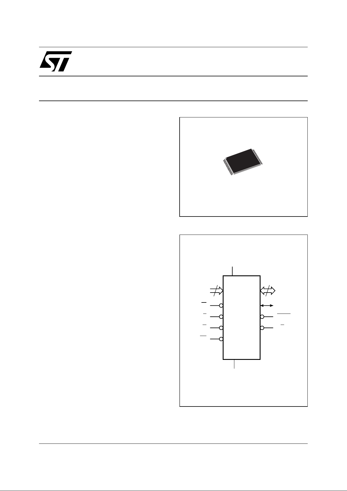
TSOP48 (N)
12 x 20mm
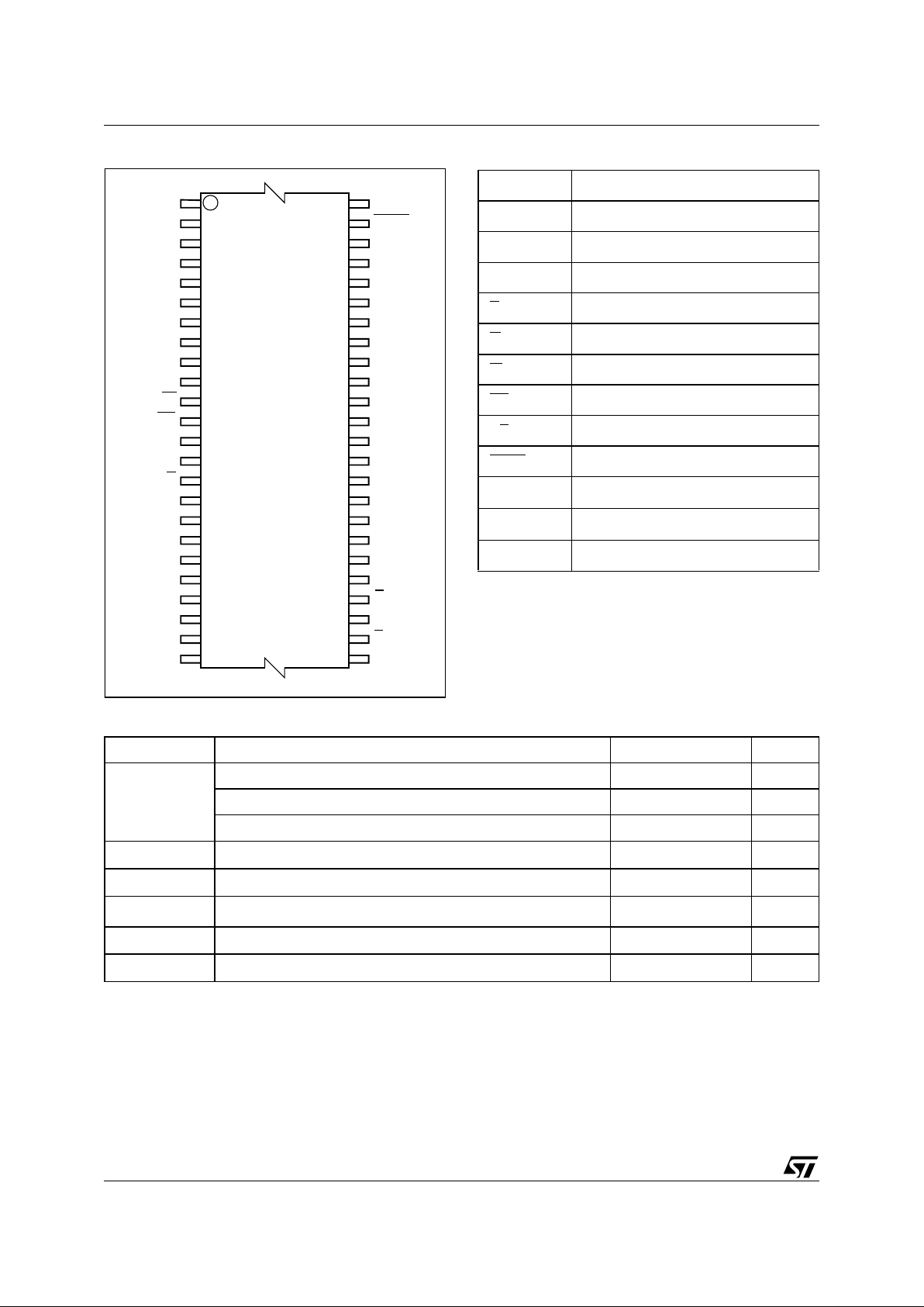
Figure 1. Logic Diagram
AI02920
20
A0-A19
W
DQ0-DQ14
V
CC
M29F160BT
M29F160BB
E
V
SS
15
G
RP
DQ15A–1
BYTE
RB
M29F160BT, M29F160BB
2/22
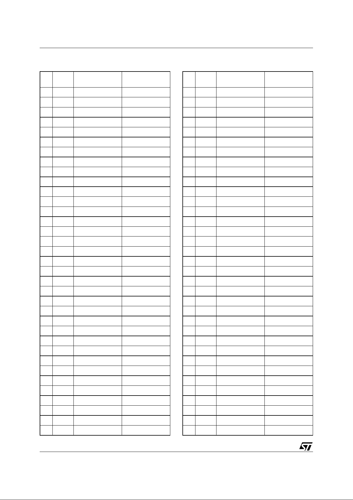
Figure 2. TSOP Connections
DQ3
DQ9
DQ2
A6
DQ0
W
A3
RB
DQ6
A8
A9
DQ13
A17
A10 DQ14
A2
DQ12
DQ10
DQ15A–1
V
CC
DQ4
DQ5
A7
DQ7
NC
NC
AI02921
M29F160BT
M29F160BB
12
1
13
24 25
36
37
48
DQ8
NC
A19
A1
A18
A4
A5
DQ1
DQ11
G
A12
A13
A16
A11
BYTE
A15
A14
V
SS
E
A0
RP
V
SS
Table 1. Signal Names
A0-A19 Address Inputs
DQ0-DQ7 Data Inputs/Outputs
DQ8-DQ14 Data Inputs/Outputs
DQ15A–1 Data Input/Output or Address Input
E
Chip Enable
G
Output Enable
W
Write Enable
RP
Reset/Block Temporary Unprotect
RB
Ready/Busy Output
BYTE
Byte/Word Organization Select
V
CC
Supply Voltage
V
SS
Ground
NC Not Connected Internally
Table 2. Absolute Maximum Ratings
(1)
Note: 1. Except for the ratin g "Operati ng Temperature Range" , stresses above those listed i n t he Table "Absolute M aximum Ratings" may
cause permanent damage to the device. These are stress ratings only and operation of the device at these or any other conditions
above those indi cated in t he Operating sect i ons of thi s specifi cation i s not impl i ed. Exposure to Absolute M aximum Rating c onditions for extended per iods may aff ect device reliabilit y. Refer also to the STMicroel ectronics SURE Program an d other relevan t qual ity docum en ts .
2. Mini m um Voltage may undershoot to –2V duri ng transit i on and for less than 20ns duri ng transitio ns.
Symbol Parameter Value Unit
T
A
Ambient Operating Temperature (Temperature Range Option 1) 0 to 70 °C
Ambient Operating Temperature (Temperature Range Option 6) –40 to 85 °C
Ambient Operating Temperature (Temperature Range Option 3) –40 to 125 °C
T
BIAS
Temperature Under Bias –50 to 125 °C
T
STG
Storage Temperature –65 to 150 °C
V
IO
(2)
Input or Output Voltage –0.6 to 6 V
V
CC
Supply Voltage –0.6 to 6 V
V
ID
Identification Voltage –0.6 to 13.5 V

3/22
M29F160BT, M29F160BB
SUMMARY DESCRIPTION
The M29F160B is a 16Mbit (2Mb x8 or 1Mb x16)
non-volatile memory that can be read, erased and
reprogrammed. These operations can be performed using a single 5V supply. On power-up the
memory defaults to its Read mode where it can be
read in the same way as a ROM or EPROM.
The memory is divided into blocks that can be
erased independently so it is pos sible to pres erve
valid data while old data is erased. Each block can
be protected independently to prev ent accidental
Program or Erase commands from modifying the
memory. Program and Erase com m ands are wri tten to the Command Interface of t he memory. An
on-chip Program/Erase Controller simplifies the
process of programming or erasing the memory by
taking care of all of the special operations that are
required to update the memory contents. The end
of a program or erase op eration can be de tected
and any error conditions identified. The command
set required to control the memory is consistent
with JEDEC standards.
The blocks in the memory are asymmetrically arranged, see Tables 3 and 4, Block Addresses. The
first or last 64 Kbytes hav e been divide d into four
additional blocks. The 16 Kbyte Boot Block can be
used for small initialization code to start the microprocessor, the two 8 Kbyte Parameter Blocks can
be used for parameter storage and the rem aining
32K is a small Main Block where the application
may be stored.
Chip Enable, Output Enable and Write Enable signals control the bus operation of the memory.
They allow simple conne ction to most m icroprocessors, often without additional logic.
The memory is offered in a TSOP48 (12 x 20mm)
package and it is supplied with all the bits eras ed
(set to ’1’).
M29F160BT, M29F160BB
4/22
Table 3. Top Boot Block Addresses
M29F160BT
#
Size
(Kbytes)
Address Range
(x8)
Address Range
(x16)
34 16 1FC000h-1FFFFFh FE000h-FFFFFh
33 8 1FA000h-1FBFFFh FD000h-FDFFFh
32 8 1F8000h-1F9FFFh FC000h-FCFFFh
31 32 1F0000h-1F7FFFh F8000h-FBFFFh
30 64 1E0000h-1EFFFFh F0000h-F7FFFh
29 64 1D0000h-1DFFFFh E8000h-EFFFFh
28 64 1C0000h-1CFFFFh E0000h-E7FFFh
27 64 1B0000h-1BFFFFh D8000h-DFFFFh
26 64 1A0000h-1AFFFFh D0000h-D7FFFh
25 64 190000h-19FFFFh C8000h-CFFFFh
24 64 180000h-18FFFFh C0000h-C7FFFh
23 64 170000h-17FFFFh B8000h-BFFFFh
22 64 160000h-16FFFFh B0000h-B7FFFh
21 64 150000h-15FFFFh A8000h-AFFFFh
20 64 140000h-14FFFFh A0000h-A7FFFh
19 64 130000h-13FFFFh 98000h-9FFFFh
18 64 120000h-12FFFFh 90000h-97FFFh
17 64 110000h-11FFFFh 88000h-8FFFFh
16 64 100000h-10FFFFh 80000h-87FFFh
15 64 0F0000h-0FFFFFh 78000h-7FFFFh
14 64 0E0000h-0EFFFFh 70000h-77FFFh
13 64 0D0000h-0DFFFFh 68000h-6FFFFh
12 64 0C0000h-0CFFFFh 60000h-67FFFh
11 64 0B0000h-0BFFFFh 58000h-5FFFFh
10 64 0A0000h-0AFFFFh 50000h-57FFFh
9 64 090000h-09FFFFh 48000h-4FFFFh
8 64 080000h-08FFFFh 40000h-47FFFh
7 64 070000h-07FFFFh 38000h-3FFFFh
6 64 060000h-06FFFFh 30000h-37FFFh
5 64 050000h-05FFFFh 28000h-2FFFFh
4 64 040000h-04FFFFh 20000h-27FFFh
3 64 030000h-03FFFFh 18000h-1FFFFh
2 64 020000h-02FFFFh 10000h-17FFFh
1 64 010000h-01FFFFh 08000h-0FFFFh
0 64 000000h-00FFFFh 00000h-07FFFh
Table 4. Bottom Boot Block Addresses
M29F160BB
#
Size
(Kbytes)
Address Range
(x8)
Address Range
(x16)
34 64 1F0000h-1FFFFFh F8000h-FFFFFh
33 64 1E0000h-1EFFFFh F0000h-F7FFFh
32 64 1D0000h-1DFFFFh E8000h-EFFFFh
31 64 1C0000h-1CFFFFh E0000h-E7FFFh
30 64 1B0000h-1BFFFFh D8000h-DFFFFh
29 64 1A0000h-1AFFFFh D0000h-D7FFFh
28 64 190000h-19FFFFh C8000h-CFFFFh
27 64 180000h-18FFFFh C0000h-C7FFFh
26 64 170000h-17FFFFh B8000h-BFFFFh
25 64 160000h-16FFFFh B0000h-B7FFFh
24 64 150000h-15FFFFh A8000h-AFFFFh
23 64 140000h-14FFFFh A0000h-A7FFFh
22 64 130000h-13FFFFh 98000h-9FFFFh
21 64 120000h-12FFFFh 90000h-97FFFh
20 64 110000h-11FFFFh 88000h-8FFFFh
19 64 100000h-10FFFFh 80000h-87FFFh
18 64 0F0000h-0FFFFFh 78000h-7FFFFh
17 64 0E0000h-0EFFFFh 70000h-77FFFh
16 64 0D0000h-0DFFFFh 68000h-6FFFFh
15 64 0C0000h-0CFFFFh 60000h-67FFFh
14 64 0B0000h-0BFFFFh 58000h-5FFFFh
13 64 0A0000h-0AFFFFh 50000h-57FFFh
12 64 090000h-09FFFFh 48000h-4FFFFh
11 64 080000h-08FFFFh 40000h-47FFFh
10 64 070000h-07FFFFh 38000h-3FFFFh
9 64 060000h-06FFFFh 30000h-37FFFh
8 64 050000h-05FFFFh 28000h-2FFFFh
7 64 040000h-04FFFFh 20000h-27FFFh
6 64 030000h-03FFFFh 18000h-1FFFFh
5 64 020000h-02FFFFh 10000h-17FFFh
4 64 010000h-01FFFFh 08000h-0FFFFh
3 32 008000h-00FFFFh 04000h-07FFFh
2 8 006000h-007FFFh 03000h-03FFFh
1 8 004000h-005FFFh 02000h-02FFFh
0 16 000000h-003FFFh 00000h-01FFFh

5/22
M29F160BT, M29F160BB
SIGNAL DESCRIPTIONS
See Figure 1, Logic Diagram, and Table 1, Sign al
Names, for a brief overview of the signals connected to this device.
Address Inputs (A0-A19). The Address Inputs
select the cells i n the memory array to a ccess during Bus Read operations. During Bus Write operations they control the commands sent to the
Command Interface of the internal state machine.
Data Inputs/Outputs (DQ0-DQ7). The Data Inputs/Outputs output the data stored at the selected
address during a Bus Read operation. During Bus
Write operations they represent the commands
sent to the Command Interface of the internal state
machine.
Data Inputs/Outputs (DQ8-DQ14). The Data Inputs/Outputs output the data stored at the selected
address during a Bus Read operation when BYTE
is High, VIH. When BYTE is Low, VIL, these pins
are not used and are high impedance. During Bus
Write operations the Command Register does not
use these bits. When reading t he Status Register
these bits should be ignored.
Data Input/Output or Address Input (DQ15A-1).
When BYTE
is High, VIH, this pin behaves as a
Data Input/Output pin (as DQ8-DQ14). When
BYTE
is Low, VIL, this pin behaves as an address
pin; DQ15A–1 Low will select the LSB of the Word
on the other addresses, DQ15A–1 High will select
the MSB. Throughout the text consider references
to the Data Input/Output to include this pin when
BYTE
is High and ref erences to the Address In-
puts to include this pin when BYTE
is Low except
when stated explicitly otherwise.
Chip Enable (E
). The Chip Enable, E, activates
the memory, allowing Bus Read and Bus Write operations to be performed. When Chip Enable is
High, V
IH
, all other pins are ignored.
Output Enable (G
). The Output Enable, G, con-
trols the Bus Read operation of the memory.
Write Enable (W
). The Write Enable, W, controls
the Bus Write operation of the memory’s Command Interf a c e .
Reset/Bloc k Tempor ary U nprot ect (RP
). The Re-
set/Block Temporary Unprotect pin can be used to
apply a Hardware Reset to the memory or to temporarily unprotect all blocks that have been protected.
A Hardware Reset is achieved by holding Reset/
Block Temporary Unprotect Low, V
IL
, for at least
t
PLPX
. After Reset/Block Temporary Unprotect
goes High, V
IH
, the memory will be ready for Bus
Read and Bus Write operations after t
PHEL
or
t
RHEL
, whichever occurs last. See the Ready/Busy
Output section, Table 17 and Figure 10, Reset/
Temporary Unprotect AC Characteristics for more
details.
Holding RP
at VID will temporarily unprotect the
protected blocks in the memory. Program and
Erase operations on all blocks will be possible.
The transition from V
IH
to VID must be slower than
t
PHPHH
.
Ready/Busy Output (RB
). The Ready/Busy pin
is an open-drain output that can be used to identify
when the memory array can be read. Ready/Busy
is high-impedance during Read mode, Auto Select
mode and Erase Suspend mode.
After a Hardware Reset, Bus Read and Bus Write
operations cannot begin until Ready/Busy becomes high-impedance. See Tabl e 17 and Figure
10, Reset/Temporary Unprotect AC Characteristics.
During Program or Erase operations Ready/Busy
is Low, V
OL
. Ready/Busy will remain Low during
Read/Reset commands or Hardw are Resets until
the memory is ready to enter Read mode.
The use of an open-drain output allows the Ready/
Busy pins from several memories to be connected
to a single pull-up resistor. A Low will then indicate
that one, or more, of the memories is busy.
Byte/Word Or ga nizat ion Select (BYTE
). The Byte/
Word Organization Select pin is used to switch between the 8-bit and 16-bit Bus modes of the memory. When Byte/Word Organi z ation S elect is Low,
V
IL
, the memory is in 8-bi t mode, w hen it is High,
V
IH
, the memory is in 16-bit mode.
V
CC
Supply Voltage. The VCC Supply Voltage
supplies the power for all operations (Read, Program, Erase etc.).
The Command Interface is disabled when the V
CC
Supply Voltage is less than the L ockout Voltage,
V
LKO
. This prevents Bus Write operations from accidentally damaging the data during power up,
power down and power surges. If the Program/
Erase Controller is programming or erasing during
this time then the operation aborts and the memory contents being altered will be invalid.
A 0.1µF capacitor should be connected between
the V
CC
Supply Voltage pin and the VSS Ground
pin to decouple the current surges from the power
supply. The PCB track widths must be sufficient to
carry the currents required during program and
erase operations, I
CC4
.
Vss Ground. The V
SS
Ground is the reference
for all voltage measurements.
M29F160BT, M29F160BB
6/22
Table 5. Bus Operations, BYTE = V
IL
Note: X = VIL or VIH.
Table 6. Bus Operations, BYTE = V
IH
Note: X = VIL or VIH.
Operation E G W
Address Inputs
DQ15A–1, A0-A1 9
Data Inputs/Outputs
DQ14-DQ8 DQ7-DQ0
Bus Read
V
IL
V
IL
V
IH
Cell Address Hi-Z Data Output
Bus Write
V
IL
V
IH
V
IL
Command Address Hi-Z Data Input
Output Disable X
V
IH
V
IH
X Hi-Z Hi-Z
Standby
V
IH
X X X Hi-Z Hi-Z
Read Manufacturer
Code
V
IL
V
IL
V
IH
A0 = VIL, A1 = VIL, A9 = VID,
Others V
IL
or V
IH
Hi-Z 20h
Read Device Code
V
IL
V
IL
V
IH
A0 = VIH, A1 = VIL, A9 = VID,
Others V
IL
or V
IH
Hi-Z
CCh (M29F160BT)
4Bh (M29F160BB)
Operation E
G W
Address Inputs
A0-A19
Data Inputs/Outputs
DQ15A–1, DQ14-DQ0
Bus Read
V
IL
V
IL
V
IH
Cell Address Data Output
Bus Write
V
IL
V
IH
V
IL
Command Address Data Input
Output Disable X
V
IH
V
IH
X Hi-Z
Standby
V
IH
X X X Hi-Z
Read Manufacturer
Code
V
IL
V
IL
V
IH
A0 = VIL, A1 = VIL, A9 = VID,
Others V
IL
or V
IH
0020h
Read Device Code
V
IL
V
IL
V
IH
A0 = VIH, A1 = VIL, A9 = VID,
Others V
IL
or V
IH
22CCh (M29F160B T)
224Bh (M29F160B B)
BUS OPERATIONS
There are five standard bus operations that control
the device. These are Bus Read, Bus Wri te, Output Disable, Standby and Automatic Standby. See
Tables 5 and 6, Bus Operat ions, for a summary.
Typically glitches of less than 5ns on Chip Enable
or Write Enable are ignored by the memory and do
not affect bus operations.
Bus Read. Bus Read operations read from the
memory cells, or specific registers in the Command Interface. A valid Bus Read operation involves setting the desired address on the Address
Inputs, applying a Low sig nal, V
IL
, to Chip Enable
and Output Enable and keeping Write Enable
High, V
IH
. The Data Inputs/Outputs will output the
value, see Figure 7, Rea d Mode AC Wav eforms,
and Table 14, Read AC Characteristics, for details
of when the output becomes valid.
Bus Write. Bus Write operations write to the
Command Interface. A valid Bus Write operation
begins by setting the desire d address on t he Address Inputs. The Address Inputs are latched by
the Command Interface on the falling edge of Chip
Enable or Write Enable, whichever occurs last.
The Data Inputs/Outputs a re latched by the Command Interface on the rising edge of Chip Enable
or Write Enable, whichever occurs first. Output Enable must remain High, V
IH
, during the whole Bus
Write operation. See Figures 8 an d 9, Write AC
Waveforms, and Tables 15 and 16, Write AC
Characteristics, for details of the timing requirements.
Output Disa bl e . The Data Inputs/Outputs are in
the high impedance s tate when Output Enable is
High, V
IH
.
Standby. When Chip Enable is High, V
IH
, the
Data Inputs/Outputs pins are placed in the highimpedance state and the Supply Current is reduced to the Standby level.
When Chip Enable is at V
IH
the Supply Current is
reduced to the TTL Standby Supply Current, I
CC2
.
To further reduce the Supply Current to the CMOS
Standby Supply Current, I
CC3
, Chip Enable should
be held within V
CC
± 0.2V. For Standby current
levels see Table 13, DC Characteristics.

7/22
M29F160BT, M29F160BB
During program or erase operations the memory
will continue to use the Program/Erase Supply
Current, I
CC4
, for Program or Erase operations un-
til the operation completes.
Auto m ati c S tan d by . If CMOS levels (V
CC
± 0.2V)
are used to drive the bus and the bus is inactive for
150ns or more the memory enters Automatic
Standby where the internal Supply Current is reduced to the CMOS Standby Supply Current, I
CC3
.
The Data In puts/Outputs will s till output data if a
Bus Read operation is in progress.
Special Bus Operations
Additional bus operations can be performed to
read the Electronic Signature and also to apply
and remove Block Protec tion. These bus operations are intended for use by programming equipment and are not usually used in applications.
They require V
ID
to be applied to some pins.
Electronic Signature. The memory has two
codes, the manufacturer code and the device
code, that can be read to identify the memory.
These codes can be read by applying t he signals
listed in Tables 5 and 6, Bus Operations.
Block Protection and Blocks Unprotection. Each
block can be separately protected against accidental Program or Erase. Protected blocks can be
unprotected to allow data to be changed.
There are two methods available for protecting
and unprotecting the blocks, one for use on programming equipment and the other for in-system
use. For further information refer to Application
Note AN1122, Applying P rotection and Unp rotection to M29 Series Flash.
COMMAND INTERFACE
All Bus Write operations t o the me mory are in terpreted by the Command Interface. Commands
consist of one or more sequential Bus Write operations. Failure to observe a valid sequence of Bus
Write operations will result in the memory returning to Read mode. The long command sequences
are imposed to maximize data security.
The address used for the commands changes depending on whether the memory is in 16-bit or 8bit mode. See either Table 7, or 8, de pending on
the configuration that is being used, for a summary
of the commands.
Read/Reset Command. The Read/Reset command returns the memory to its Read mode where
it behaves like a ROM or EPROM. It also resets
the errors in the Status Register. Either one or
three Bus Write operations can be u sed to issue
the Read/Reset command.
If the Read/Reset command is issued during a
Block Erase operation or following a Programming
or Erase error then the memory will take upto 10
µs
to abort. During the abort period no valid data can
be read from the memory. Issuing a Read/Reset
command during a Block Erase operation will
leave invalid data in the memory.
Auto Select Command. The Auto Select command is used to read the Manufacturer Code, the
Device Code and the Block Protection Status.
Three consecutive Bus Write operations are required to issue the Auto Select command. Once
the Auto Select comma nd is issued the memory
remains in Auto Select mode unt il another command is issued.
From the Auto Select mode the Manufacturer
Code can be read using a Bus Read operation
with A0 = V
IL
and A1 = VIL. The other address bits
may be set to either V
IL
or VIH. The Manufa cturer
Code for STMicroelectronics is 0020h.
The Device Code can be read using a B us Read
operation with A0 = V
IH
and A1 = VIL. The other
address bits may be set to e ither V
IL
or VIH. The
Device Code for the M29F160BT is 22CCh and for
the M29F160BB is 224Bh.
The Block Protecti on St at us of e ac h bl ock can be
read using a Bus Rea d operation with A0 = V
IL
,
A1 = V
IH
, and A12-A19 specifying the add ress of
the block. The other address bits may be set to either V
IL
or VIH. If the addressed block is protected
then 01h is output o n Data Inputs/Outputs DQ0DQ7, otherwise 00h is output.
Program Command. The Program command
can be used to program a value to one address in
the memory array at a time. The command requires four Bus Write operations, the final write operation latches the address and data in the internal
state machine and starts the Program/Erase Controller.
If the address falls in a pro tected block then the
Program command is ignored, the data remains
unchanged. The Status Register is never read and
no error condition is given.
During the program operat ion the memo ry will ignore all commands. I t is n ot poss ible t o iss ue any
command to abort or pause the operation. Typical
program times are given in Table 9. Bus Read operations during the program o peration will output
the Status Register on the Data Inputs/Outputs.
See the section on the S tatus Register for more
details.
After the program operation has completed the
memory will return to the Read mode, unle ss an
error has occurred. When an error occurs the
memory will continue to output the Status Register. A Read/Reset command must be issued to reset the error condition and return to Read mode.
Note that the Program command cannot change a
bit set at ’0’ bac k to ’1’. One of the E rase Commands must be used to set all the bits in a block or
in the whole memory from ’0’ to ’1’.
 Loading...