

1 Mbit (64Kb x16, Boot Block) Single Supply Flash Memory
■ SINGLE 5V±10% SUPPLY VOLTAGE for
PROGRAM, ERASE and READ OPERATIONS
■ ACCESS TIME: 35ns
■ PROGRAMMING TIME
–8µs per Word typical
■ 5 MEMORY BLOCKS
– 1 Boot Block (Bottom Location)
– 2 Parameter and 2 Main Blocks
■ PROGRAM/ERASE CONTROLLER
– Embedded Word Program algorithm
– Embedded Multi-Block/Chip Erase algorithm
– Status Register Polling and Toggle Bits
■ ERASE SUSPEND and RESUME MODES
– Read and Program another Block during
Erase Suspend
■ UNLOCK BYPASS PROGRAM COMMAND
– Faster Production/Batch Programming
■ TEMPORARY BLOCK UNPROTECTION
MODE
■ LOW POWERCONSUMPTION
– Standby and Automatic Standby
■ 100,000 PROGRAM/ERASE CYCLESper
BLOCK
■ M28F102 COMPATIBLE
– Pin-out and Read Mode
■ 20 YEARS DATA RETENTION
– Defectivity below 1 ppm/year
■ ELECTRONIC SIGNATURE
– Manufacturer Code: 0020h
– Device Code: 0097h
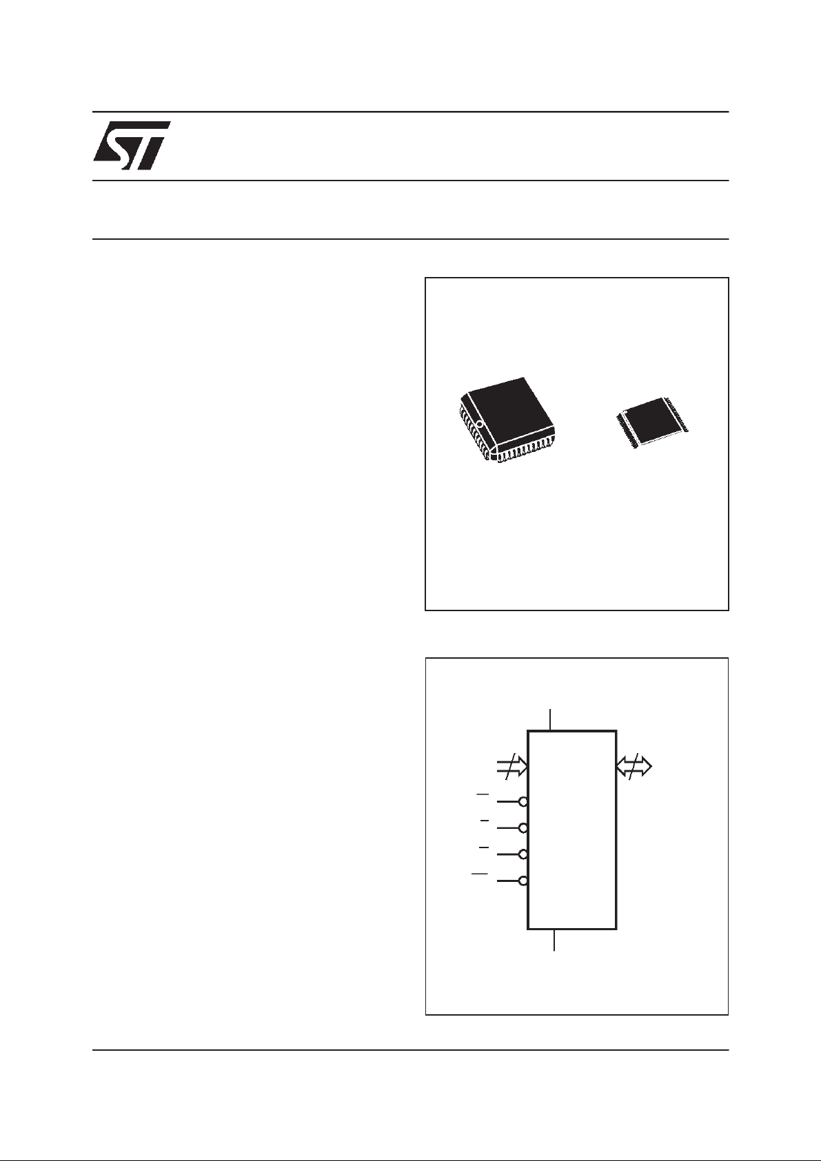
PLCC44 (K)
Figure 1. Logic Diagram
A0-A15
W
E
G
RP
16
V
CC
M29F102BB
M29F102BB
TSOP40 (N)
10 x 14mm
16
DQ0-DQ15
V
SS
AI02130C
1/20July 1999
M29F102BB
Figure 2A. PLCC Connections
RP
G
23
CC
NC
W
V
1
44
A0
A1
NC
DQ15
DQ13
DQ14
E
DQ12
DQ11
DQ10
DQ9 A10
DQ8
V
SS
NC
DQ6
DQ5
DQ4
12
DQ3
DQ2
DQ1
M29F102BB
DQ0
NC
A2
A15
A3
A14
34
A4
AI02131C
A13
A12
A11
A9
V
SS
NC
A8DQ7
A7
A6
A5
Figure 2B. TSOP Connections
A9
A10
A11
A12 A6
A13
A14
A15
NC
V
CC
RP
DQ15
DQ14
DQ13
DQ12
DQ11
DQ10
DQ9
DQ8
1
W
10
M29F102BB
11
E
20 21
AI02132C
40
31
30
V
SS
A8
A7
A5
A4
A3
A2
A1
A0
G
DQ0
DQ1
DQ2
DQ3
DQ4
DQ5
DQ6
DQ7
V
SS
Table 1. Signal Names
A0-A15 Address Inputs
DQ0-DQ15 Data Inputs/Outputs
E Chip Enable
G Output Enable
W Write Enable
RP Reset/Block Temporary Unprotect
V
CC
V
SS
NC Not Connected Internally
Supply Voltage
Ground
SUMMARY DESCRIPTION
The M29F102BB is a 1 Mbit (64Kb x16) non-volatile memory that can be read, erased and reprogrammed. These operations can be performed
using a single 5V supply. On power-up the memory defaults to its Read mode where it can be read
in the same way as a ROM or EPROM.
The memory is divided into blocks that can be
erased independently so it is possible to preserve
valid data while old data is erased. Each block can
be protected independently to prevent accidental
Program or Erase commands from modifying the
memory. Program and Erase commands are written to the Command Interface of the memory. An
on-chip Program/Erase Controller simplifies the
2/20

M29F102BB
Table 2. Absolute Maximum Ratings
Symbol Parameter Value Unit
T
A
T
BIAS
T
STG
(2)
V
IO
V
CC
V
ID
Note: 1. Except for the rating ”Operating Temperature Range”, stresses above those listed in the Table ”Absolute Maximum Ratings” may
cause permanent damage to the device. These are stress ratings only and operation of the device at these or any other conditions
above those indicated in the Operating sections of this specification is not implied. Exposure to Absolute Maximum Rating conditions for extended periodsmay affect device reliability. Refer also tothe STMicroelectronics SUREProgram and other relevant quality documents.
2. Minimum Voltage may undershoot to –2V during transition and for less than 20ns during transitions.
Ambient Operating Temperature 0 to 70 °C
Temperature Under Bias –50 to 125 °C
Storage Temperature –65 to 150 °C
Input or Output Voltage –0.6 to 6 V
Supply Voltage –0.6 to 6 V
Identification Voltage –0.6 to 13.5 V
process ofprogramming or erasing the memory by
taking care of all of the special operations that are
required to update the memory contents. The end
of a program or erase operation can be detected
and any error conditions identified. The command
set required to control the memory is consistent
with JEDEC standards.
The blocks in the memory are asymmetrically arranged, seeTable 3, Block Addresses. The first 32
Kwords have been divided into four additional
blocks. The 8 Kword Boot Block can be used for
small initialization code to start the microprocessor, the two 4 Kword Parameter Blocks can be
used for parameter storage and the remaining 16
Kwords are a small Main Block where the application may be stored.
Chip Enable, Output Enable and Write Enable signals control the bus operation of the memory.
They allow simple connection to most microprocessors, often without additional logic.
The memory is offered in PLCC44 and TSOP40
(10 x 14mm) packages. Access times of 35ns,
45ns, 50ns, 55ns and 70ns are available. The
memory is supplied with all thebits erased (set to
’1’).
(1)
SIGNAL DESCRIPTIONS
See Figure 1, Logic Diagram, and Table 1, Signal
Names, for a brief overview of the signals connected to this device.
Address Inputs (A0-A15). The Address Inputs
select the cells in the memory array to access during Bus Read operations. During Bus Write operations they control the commands sent to the
Command Interface of the internal state machine.
Data Inputs/Outputs (DQ0-DQ15). The Data Inputs/Outputs output thedata stored attheselected
address during a Bus Read operation. During Bus
Write operations DQ0-DQ7 represent the commands sent to the Command Interface ofthe internal state machine; the Command Interface does
not use DQ8-DQ15 to decode the commands.
Chip Enable (E). The Chip Enable, E, activates
the memory, allowing Bus Read and Bus Write operations to be performed. When Chip Enable is
High, VIH, all other pins are ignored.
Output Enable (G). The Output Enable, G, controls the Bus Read operation of the memory.
Write Enable (W). The Write Enable, W, controls
the Bus Write operation of the memory’s Command Interface.
3/20

M29F102BB
Table 3. Block Addresses
Size (KWords) Address Range
32 8000h-FFFFh
16 4000h-7FFFh
4 3000h-3FFFh
4 2000h-2FFFh
8 0000h-1FFFh
Reset/BlockTemporaryUnprotect (RP). The Reset/Block Temporary Unprotect pin can be used to
apply a Hardware Reset to the memory or to temporarily unprotect all blocks that have been protected.
A Hardware Reset is achieved by holding Reset/
Block Temporary Unprotect Low, VIL, for at least
t
. After Reset/Block Temporary Unprotect
PLPX
goes High, VIH, the memory will be ready for Bus
Read and Bus Write operations after t
or t
, whichever occurs last. See Table 13 and
PLYH
PHEL
Figure 10, Reset/Temporary Unprotect AC Characteristics for more details.
Holding RP at VIDwill temporarily unprotect the
protected blocks in the memory. Program and
Erase operations on all blocks will be possible.
The transition from VIHtoVIDmust be slower than
t
PHPHH
.
Reset/Block Temporary Unprotect can be left unconnected. A weak internal pull-up resistor ensures that the memory always operates correctly.
VCCSupply Voltage. The VCCSupply Voltage
supplies the power for all operations (Read, Program, Erase etc.).
The Command Interface is disabled when the V
CC
Supply Voltage is less than the Lockout Voltage,
V
. This prevents Bus Write operations from ac-
LKO
cidentally damaging the data during power up,
power down and power surges. If the Program/
Erase Controller is programming or erasing during
this time then the operation aborts and the memory contents being altered will be invalid.
A 0.1µF capacitor should be connected between
the VCCSupply Voltage pin and the VSSGround
pin to decouple the current surges from the power
supply. The PCB track widths must be sufficient to
carry the currents required during program and
erase operations, I
CC3
.
Vss Ground. The VSSGround is the reference
for all voltage measurements.
BUS OPERATIONS
There arefive standard bus operations that control
the device. These are Bus Read, Bus Write, Output Disable,Standby and Automatic Standby. See
Table 4, Bus Operations, for a summary. Typically
glitches of less than 5ns on Chip Enable or Write
Enable are ignored by the memory and do not affect bus operations.
Bus Read. Bus Read operations read from the
memory cells, or specific registers in the Command Interface. A valid Bus Read operation involves setting the desired address on the Address
Inputs, applying a Low signal, VIL, to Chip Enable
and Output Enable and keeping Write Enable
High, VIH. The Data Inputs/Outputs will output the
value, see Figure 7, Read Mode AC Waveforms,
and Table 11, Read AC Characteristics, fordetails
of when the output becomes valid.
Bus Write. Bus Write operations write to the
Command Interface. A valid Bus Write operation
begins by setting the desired address on the Address Inputs. The Address Inputs are latched by
the Command Interface on the falling edge of Chip
Enable or Write Enable, whichever occurs last.
The Data Inputs/Outputs are latched by the Command Interface on the rising edge of Chip Enable
or Write Enable, whichever occursfirst.OutputEnable must remain High, VIH, during the whole Bus
Write operation. See Figures 8 and 9, Write AC
Waveforms, and Tables 12 and 13, Write AC
4/20
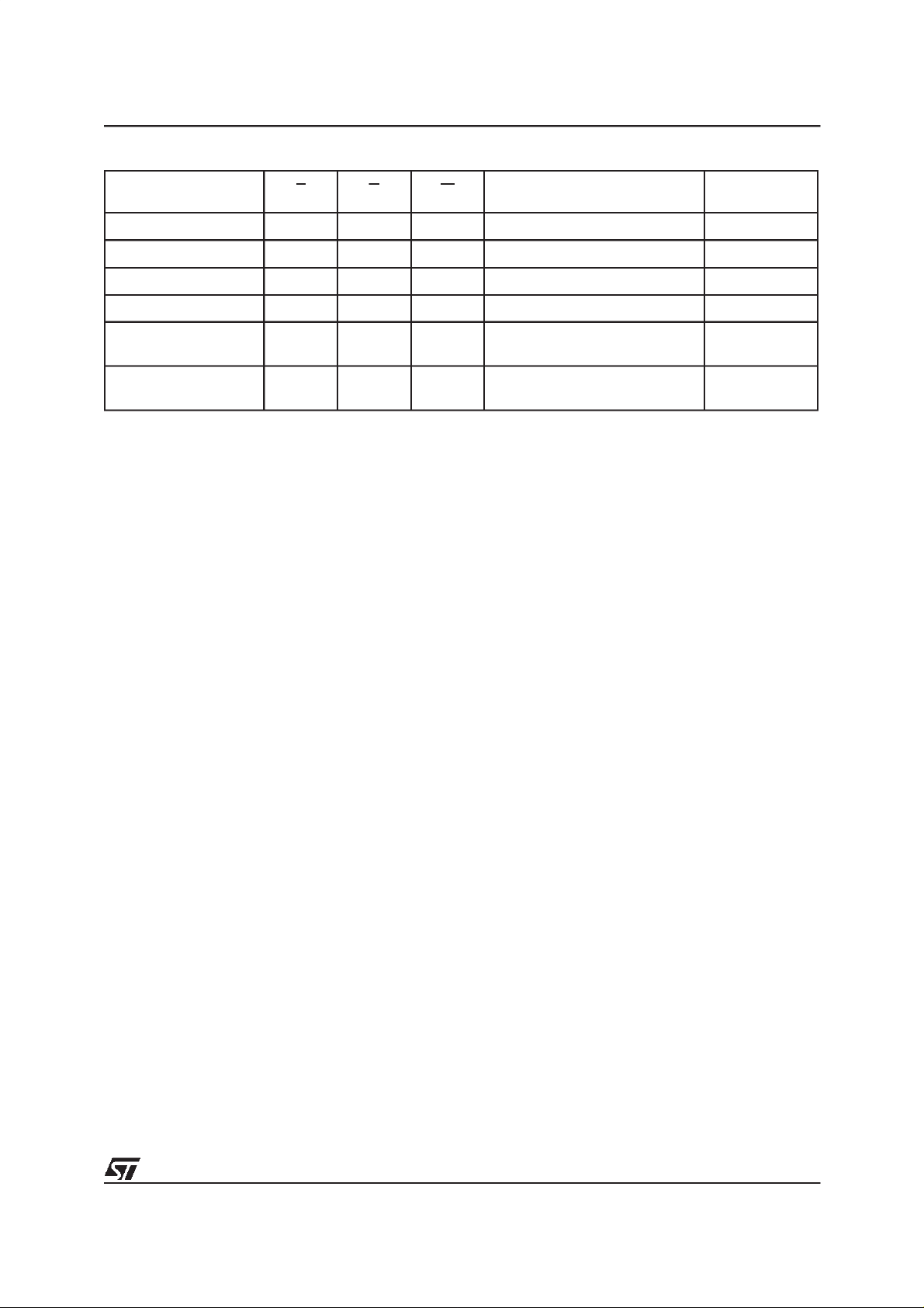
Table 4. Bus Operations
Operation E G W Address Inputs
Bus Read
Bus Write
Output Disable X
Standby
Read Manufacturer
Code
Read Device Code V
Note: X = VILor VIH.
M29F102BB
Data
Inputs/Outpu ts
V
IL
V
IL
V
IH
V
IL
IL
V
IL
V
IH
V
IH
XXX Hi-Z
V
IL
V
IL
V
V
V
V
V
Cell Address Data Output
IH
Command Address Data Input
IL
XHi-Z
IH
A0 = VIL,A1=VIL,A9=VID,
IH
Others V
A0 = VIH,A1=VIL,A9=VID,
IH
Others V
or V
IL
or V
IL
IH
IH
0020h
0097h
Characteristics, for details of the timing requirements.
Output Disable. The Data Inputs/Outputs are in
the high impedance state when Output Enable is
High, VIH.
Standby. When Chip Enable is High, VIH, the
memory enters Standby mode and the Data Inputs/Outputs pins are placed in the high-impedance state. To reduce the Supply Current to the
Standby Supply Current, I
, ChipEnableshould
CC2
be held within VCC± 0.2V. For the Standby current
level see Table 10, DC Characteristics.
During program or erase operations the memory
will continue to use the Program/Erase Supply
Current, I
, for Program or Erase operations un-
CC3
til the operation completes.
AutomaticStandby. If CMOS levels (VCC± 0.2V)
are usedto drive the bus and the busis inactive for
150ns or more the memory enters Automatic
Standby where the internal Supply Current is reduced to the Standby Supply Current, I
CC2
. The
Data Inputs/Outputs will still output data if a Bus
Read operation is in progress.
Special Bus Operations
Additional bus operations can be performed to
read the Electronic Signature and also to apply
and remove Block Protection. These bus operations are intended for use by programming equipment and are not usually used in applications.
They require VIDto be applied to some pins.
Electronic Signature. The memory has two
codes, the manufacturer code and the device
code, that can be read to identify the memory.
These codes can be read by applying the signals
listed in Table 4, Bus Operations.
BlockProtection and BlocksUnprotection. Each
block can be separately protected against accidental Program or Erase. Protected blocks can be
unprotected to allow data to be changed.
There are two methods available for protecting
and unprotecting the blocks, one for use on programming equipment and the other for in-system
use. For further information refer to Application
Note AN1122, Applying Protection and Unprotection to M29 Series Flash.
5/20

M29F102BB
COMMAND INTERFACE
All Bus Write operations to the memory are interpreted by the Command Interface. Commands
consist of one or more sequential Bus Write operations. Failure to observe a valid sequence of Bus
Write operations will result in the memory returning to Read mode. The long command sequences
are imposed to maximize data security.
The commands are summarized in Table 5, Commands. Refer to Table 5 in conjunction with the
text descriptions below.
Read/Reset Command. The Read/Reset command returns the memory to its Read mode where
it behaves like a ROM or EPROM. It also resets
the errors in the Status Register. Either one or
three Bus Write operations can be used to issue
the Read/Reset command.
If the Read/Reset command is issued during a
Block Erase operation or following a Programming
or Erase error then the memory will take upto 10µs
to abort. During the abort period no valid data can
be read from the memory. Issuing a Read/Reset
command during a Block Erase operation will
leave invalid data in the memory.
Auto Select Command. The Auto Select command is used to read the Manufacturer Code, the
Device Code and the Block Protection Status.
Three consecutive Bus Write operations are required to issue the Auto Select command. Once
the Auto Select command is issued the memory
remains in Auto Select mode until another command is issued.
From the Auto Select mode the Manufacturer
Code can be read using a Bus Read operation
with A0 = VILand A1 = VIL. The otheraddress bits
may be set to either VILor VIH. The Manufacturer
Code for STMicroelectronics is 0020h.
The Device Code can be read using a Bus Read
operation with A0 = VIHand A1 = VIL. The other
address bits may be set to either VILor VIH.The
Device Code for the M29F102BB is 0097h.
The Block Protection Status of each block can be
read using a Bus Read operation with A0 = VIL,
A1 = VIH, and A12-A15 specifying the address of
the block. The otheraddress bits may be set toeither VILorVIH. If the addressed block is protected
then 01h is output on Data Inputs/Outputs
DQ0-DQ7, otherwise 00h is output.
Program Command. The Program command
can be used to program a value to one address in
the memory array at a time. The command requires fourBus Write operations, the final write operation latches theaddress and data intheinternal
state machine and starts the Program/Erase Controller.
If the address falls in a protected block then the
Program command is ignored, the data remains
unchanged. The Status Register is never read and
no error condition is given.
During the program operation the memory will ignore all commands. It is not possible to issue any
command to abort or pause the operation. Typical
program timesare given in Table 6. Bus Read operations during the program operation will output
the Status Register on the Data Inputs/Outputs.
See the section on the Status Register for more
details.
After the program operation has completed the
memory will return to the Read mode, unless an
error has occurred. When an error occurs the
memory will continue to output the Status Register. A Read/Reset command must be issued to reset the error condition and return to Read mode.
Note thatthe Program command cannot change a
bit set at ’0’ back to ’1’ and attempting to do so will
cause an error.One of the Erase Commands must
be used to set all the bits in a block or in the whole
memory from ’0’ to ’1’.
Unlock Bypass Command. The Unlock Bypass
command is used in conjunction with the Unlock
Bypass Program command to program the memory. When the access time to the device is long (as
with some EPROM programmers) considerable
time saving can be made by using these commands. Three Bus Write operations are required
to issue the Unlock Bypass command.
Once the Unlock Bypass command has been issued the memory will only accept the Unlock Bypass Program command and the Unlock Bypass
Reset command. The memory can be read as if in
Read mode.
Unlock Bypass Program Command. The Un-
lock Bypass Program command can be used to
program one address in memory at a time. The
command requires two Bus Write operations, the
final write operation latches the address and data
in the internal state machine and starts the Program/Erase Controller.
The Program operation using the Unlock Bypass
Program command behaves identically to the Program operation using the Program command. A
protected block cannot be programmed; the operation cannot be abortedand the Status Register is
read. Errors must be reset using the Read/Reset
command, which leaves the device in Unlock Bypass Mode. See the Program command for details
on the behavior.
6/20
 Loading...