

1/21April 2000
M29F080A
8 Mbit (1Mb x8, Uniform Block) Single Supply Flash Memory
■ SINGLE 5V±10% SUPPLY VOLTAGE for
PROGRAM, ERASE and READ OPERATIONS
■ ACCESS TIME: 70ns
■ PROGRAMMING TIME
–8µs by Byte typical
■ 16 UNIFORM 64 Kbyte MEMORY BLOCKS
■ PROGRAM/ERASE CONTROLLER
– Embedded Byte Program algorithm
– Embedded Multi-Block/Chip Erase algorithm
– Status Register Polling and Toggle Bits
– Ready/Busy Output Pin
■ ERASE SUSPEND and RESUME MODES
– Read and Program another Block during
Erase Suspend
■ TEMPORARY BLOCK UNPROTECTION
MODE
■ LOW POWER CONSUMPTION
– Standby and Automatic Standby
■ 100,000 PROGRAM/ERASE CYCLES per
BLOCK
■ 20 YEARS DATA RETENTION
– Defectivity below 1 ppm/year
■ ELECTRONIC SIGNATURE
– Manufacturer Code: 20h
– Device Code: F1h
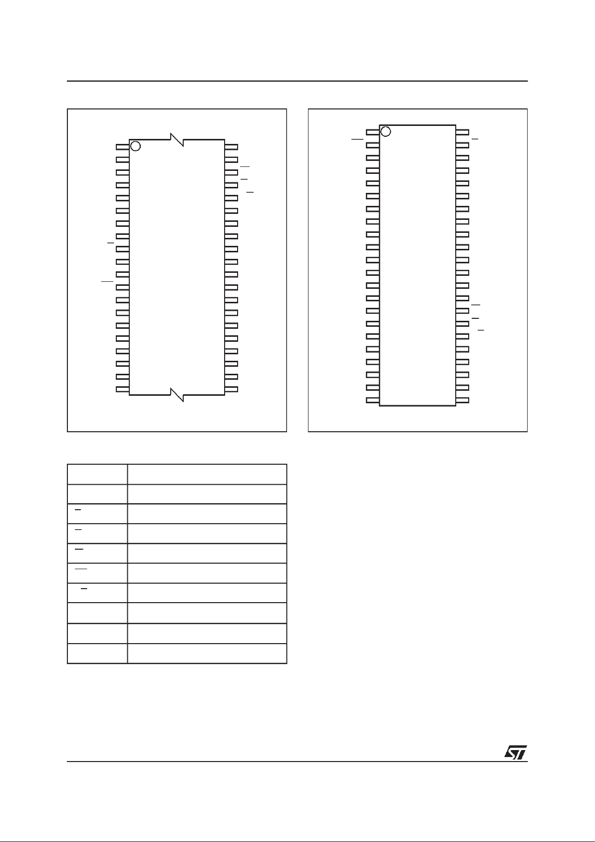
TSOP40 (N)
10 x 20mm
SO44 (M)
44
1
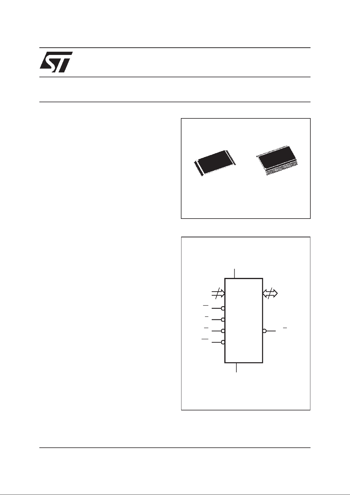
Figure 1. Logic Diagram
AI00501C
20
A0-A19
W
DQ0-DQ7
V
CC
M29F080A
E
V
SS
8
G
RP
RB
M29F080A
2/21
Figure 2. TSOP Connections
A1
DQ1
DQ2A10
A4
A2
A7
A6
A14
NC
A17
A18
DQ7
A13
A19
A0
W
DQ5
DQ3
V
SS
V
CC
DQ4
DQ6
A12
E
RP
A11
NC
V
CC
AI00520B
M29F080A
10
1
11
20 21
30
31
40
A3
A15
A16 G
RB
A8
A9
V
SS
DQ0
NC
A5
Figure 3. SO Connections
A2
A1
A0
A6
NC
NC
A3
A5
A4
A17
NC
A18
A19
W
A16
NC
NC
NC
DQ6DQ2
V
SS
V
CC
V
SS
DQ4
G
A13
E
NC
A7
RP
V
CC
A10
AI00521B
M29F080A
8
2
3
4
5
6
7
9
10
11
12
13
14
15
16
32
31
30
29
28
27
26
25
24
2322
20
19
18
17DQ0
DQ1
A9
A8
RB
DQ7
44
39
38
37
36
35
34
33
A15
A14
DQ3
21
DQ5
40
43
1
42
41
A11 A12
Table 1. Signal Names
A0-A19 Address Inputs
DQ0-DQ7 Data Inputs/Outputs
E Chip Enable
G Output Enable
W Write Enable
RP Reset/Block Temporary Unprotect
RB Ready/Busy Output
V
CC
Supply Voltage
V
SS
Ground
NC Not Connected Internally
SUMMARY DESCRIPTION
The M29F080A is an 8 Mbit (1Mb x8) non-volatile
memory that can be read, erased and reprogrammed. These operations can be performedus-
ing a single 5V supply. On power-up the memory
defaults to its Read mode where it can be read in
the same way as a ROM or EPROM.
The memory is divided into blocks that can be
erased independently so it is possible to preserve
valid data while old data is erased. Blocks can be
protected in groups to prevent accidental Program
or Erase commands from modifying the memory.
Program and Erase commands are written to the
Command Interface of the memory. An on-chip
Program/Erase Controllersimplifiestheprocessof
programming or erasing the memory by taking
care of all of the special operations that are required to update the memory contents. The end of
a program or eraseoperation can be detected and
any error conditions identified. The command set
required to control the memory is consistent with
JEDEC standards.
Chip Enable, Output Enableand Write Enable signals control the bus operation of the memory.
They allow simple connection to most microprocessors, often without additional logic.
The memory is offered in a TSOP40 (10 x 20mm)
and SO44 packages and it is supplied with all the
bits erased (set to ’1’).
3/21
M29F080A
SIGNAL DESCRIPTIONS
See Figure 1, Logic Diagram, and Table 1, Signal
Names, forabrief overview of the signals connected to this device.
Address Inputs (A0-A19). The Address Inputs
select the cells in the memory array to access during Bus Read operations. During BusWrite operations they control the commands sent to the
Command Interface of the internal state machine.
Data Inputs/Outputs (DQ0-DQ7). The Data Inputs/Outputs output thedatastoredatthe selected
address during a Bus Read operation. During Bus
Write operations they represent the commands
sentto theCommandInterfaceof the internal state
machine.
Chip Enable (E). The Chip Enable, E, activates
the memory, allowing Bus Read and Bus Write operations to be performed. When Chip Enable is
High, VIH, all other pins are ignored.
Output Enable (G). The Output Enable, G, controls the Bus Read operation of the memory.
Write Enable (W). The Write Enable, W, controls
the Bus Write operation of the memory’s Command Interface.
Reset/Block TemporaryUnprotect (RP). The Reset/Block Temporary Unprotect pin can be usedto
apply a Hardware Reset to the memory or to temporarily unprotect all blocks that have been protected.
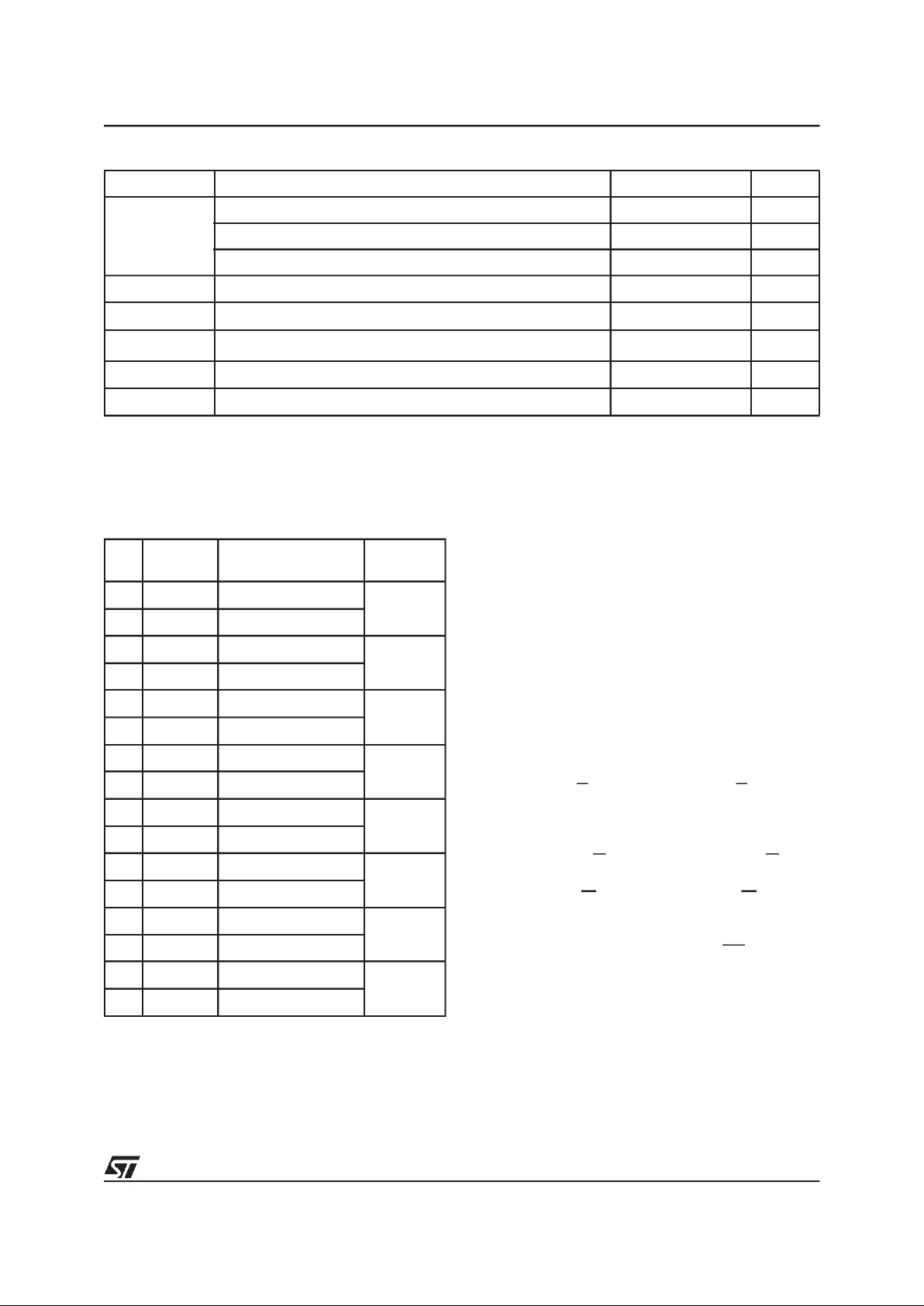
Table 2. Absolute Maximum Ratings
(1)
Note: 1. Except for the rating ”Operating Temperature Range”, stresses above those listed in the Table ”Absolute Maximum Ratings” may
cause permanent damage to the device. These are stress ratings only and operation of the device at these or any other conditions
above those indicated in the Operating sections of this specification is not implied. Exposure to Absolute Maximum Rating conditions for extended periods may affect device reliability. Refer also to the STMicroelectronics SUREProgram andotherrelevant quality documents.
2. Minimum Voltage may undershoot to –2V during transition and for less than 20ns during transitions.
Symbol Parameter Value Unit
T
A
Ambient Operating Temperature (Temperature Range Option 1) 0 to 70 °C
Ambient Operating Temperature (Temperature Range Option 6) –40 to 85 °C
Ambient Operating Temperature (Temperature Range Option 3) –40 to 125 °C
T
BIAS
Temperature Under Bias –50 to 125 °C
T
STG
Storage Temperature –65 to 150 °C
V
IO
(2)
Input or Output Voltage –0.6 to 6 V
V
CC
Supply Voltage –0.6 to 6 V
V
ID
Identification Voltage –0.6 to 13.5 V
Table 3. Uniform Block Addresses, M29F080A
#
Size
(Kbytes)
Address Range
Protection
Group
15 64 F0000h-FFFFFh
7
14 64 E0000h-EFFFFh
13 64 D0000h-DFFFFh
6
12 64 C0000h-CFFFFh
11 64 B0000h-BFFFFh
5
10 64 A0000h-AFFFFh
9 64 90000h-9FFFFh
4
8 64 80000h-8FFFFh
7 64 70000h-7FFFFh
3
6 64 60000h-6FFFFh
5 64 50000h-5FFFFh
2
4 64 40000h-4FFFFh
3 64 30000h-3FFFFh
1
2 64 20000h-2FFFFh
1 64 10000h-1FFFFh
0
0 64 00000h-0FFFFh

M29F080A
4/21
A 0.1µF capacitor should be connected between
the VCCSupply Voltage pin and the VSSGround
pin to decouple the current surges from the power
supply. The PCB track widths must be sufficient to
carry the currents required during program and
erase operations, I
CC4
.
VSSGround. The VSSGroundis the reference for
all voltage measurements.
BUS OPERATIONS
There arefive standard busoperations that control
the device. These are Bus Read, Bus Write, Output Disable, Standby and Automatic Standby. See
Table 4, Bus Operations, for asummary. Typically
glitches of less than 5ns on Chip Enable or Write
Enable are ignored by the memory and do not affect bus operations.
Bus Read. Bus Read operations read from the
memory cells, or specific registers in the Command Interface. A valid Bus Read operation involves setting the desired address on the Address
Inputs, applying a Low signal, VIL, to Chip Enable
and Output Enable and keeping Write Enable
High, VIH. The Data Inputs/Outputs will output the
value, see Figure 8, Read Mode AC Waveforms,
and Table 11, Read AC Characteristics, for details
of when the output becomes valid.
Bus Write. Bus Write operations write to the
Command Interface. A valid Bus Write operation
begins by setting the desired address on the Address Inputs. The Address Inputs are latched by
the Command Interface on the falling edge of Chip
Enable or Write Enable, whichever occurs last.
The Data Inputs/Outputs are latched by the Command Interface on the rising edge of Chip Enable
or WriteEnable, whichever occurs first. OutputEnable must remain High, VIH, during the whole Bus
Write operation. See Figures 9 and 10, Write AC
Waveforms, and Tables 12 and 13, Write AC
Characteristics, for details of the timing requirements.
A Hardware Reset is achieved by holding Reset/
Block Temporary Unprotect Low, VIL, for at least
t
PLPX
. After Reset/Block Temporary Unprotect
goes High, VIH, the memory will be ready for Bus
Read and Bus Write operations after t
PHEL
or
t
RHEL
, whicheveroccurs last.See the Ready/Busy
Output section, Table 14 and Figure 11, Reset/
Temporary Unprotect AC Characteristics for more
details.
Holding RP at VIDwill temporarily unprotect the
protected blocks in the memory. Program and
Erase operations on all blocks will be possible.
The transition from VIHtoVIDmust be slower than
t
PHPHH
.
Ready/Busy Output (RB). The Ready/Busy pin
is anopen-drain outputthat can be used toidentify
when the memory array can be read. Ready/Busy
is high-impedanceduring Read mode, Auto Select
mode and Erase Suspend mode.
After a Hardware Reset, Bus Read and Bus Write
operations cannot begin until Ready/Busy becomes high-impedance. See Table 14 and Figure
11, Reset/Temporary Unprotect AC Characteristics.
During Program or Erase operations Ready/Busy
is Low, VOL. Ready/Busy will remain Low during
Read/Reset commands or Hardware Resets until
the memory is ready to enter Read mode.
The use of an open-drain output allows the Ready/
Busy pins from several memories to be connected
to a single pull-up resistor. A Low will then indicate
that one, or more, of the memories is busy.
VCCSupply Voltage. The VCCSupply Voltage
supplies the power for all operations (Read, Program, Erase etc.).
The CommandInterface is disabled when the V
CC
Supply Voltage is less than the Lockout Voltage,
V
LKO
. This prevents Bus Write operations from accidentally damaging the data during power up,
power down and power surges. If the Program/
Erase Controller is programming or erasing during
this time then the operation aborts and the memory contents being altered will be invalid.
5/21
M29F080A
Table 4. Bus Operations
Note: X = VILor VIH.
Operation E G W Address Inputs
Data
Inputs/Outpu ts
Bus Read
V
IL
V
IL
V
IH
Cell Address Data Output
Bus Write
V
IL
V
IH
V
IL
Command Address Data Input
Output Disable
XV
IH
V
IH
XHi-Z
Standby
V
IH
XXX Hi-Z
Read Manufacturer
Code
V
IL
V
IL
V
IH
A0 = VIL,A1=VIL,A9=VID,
Others V
IL
or V
IH
20h
Read Device Code
V
IL
V
IL
V
IH
A0 = VIH,A1=VIL,A9=VID,
Others V
IL
or V
IH
F1h
Output Disable. The Data Inputs/Outputs are in
the high impedance state when Output Enable is
High, VIH.
Standby. When Chip Enable is High, VIH, the
Data Inputs/Outputs pins are placed in the highimpedance state and the Supply Current is reduced to the Standby level.
When Chip Enable is at VIHthe Supply Current is
reduced to the TTL Standby Supply Current, I
CC2
.
To further reduce the Supply Current to the CMOS
Standby Supply Current, I
CC3
, ChipEnable should
be held within VCC± 0.2V. For Standby current
levels see Table 10, DC Characteristics.
During program or erase operations the memory
will continue to use the Program/Erase Supply
Current, I
CC4
, for Program or Eraseoperations un-
til the operation completes.
AutomaticStandby. If CMOS levels (VCC± 0.2V)
are usedto drive the bus and the bus is inactive for
150ns or more the memory enters Automatic
Standby where the internal Supply Current is reduced to the Standby Supply Current, I
CC3
. The
Data Inputs/Outputs will still output data if a Bus
Read operation is in progress.
Special Bus Operations
Additional bus operations can be performed to
read the Electronic Signature and also to apply
and remove Block Protection. These bus operations are intended for use by programming equipment and are not usually used in applications.
They require VIDto be applied to some pins.
Electronic Signature. The memory has two
codes, the manufacturer code and the device
code, that can be read to identify the memory.
These codes can be read by applying the signals
listed in Table 4, Bus Operations.
Block Protection and BlocksUnprotection. Blocks
can be protected in groups against accidental Program or Erase. See Table 3, Block Addresses, for
details of which blocks must be protected together
as a group. Protected blocks can be unprotected
to allow data to be changed. Block Protection and
Block Unprotection operations must only be performed on programming equipment.
For further information refer to Application Note
AN1122, Applying Protection and Unprotection to
M29 Series Flash.

M29F080A
6/21
COMMAND INTERFACE
All Bus Write operations to the memory are interpreted by the Command Interface. Commands
consist of one or more sequential Bus Write operations. Failure to observe a validsequence of Bus
Write operations will result in the memory returning toRead mode. In this case, after at least 50ns,
an address transition or Chip Enable going Low is
required before reading correct data. The long
command sequences are imposed to maximize
data security.
The commands are summarized in Table 5, Commands. Refer to Table 5 in conjunction with the
text descriptions below.
Read/Reset Command. The Read/Reset command returnsthe memory to its Read mode where
it behaves like a ROM or EPROM. It also resets
the errors in the Status Register. Either one or
three Bus Write operations can be used to issue
the Read/Reset command.
If the Read/Reset command is issued during a
Block Eraseoperation or following a Programming
or Eraseerror thenthe memory will takeup to10µs
to abort. During the abort period no valid data can
be read from the memory. Issuing a Read/Reset
command during a Block Erase operation will
leave invalid data in the memory.
Auto Select Command. The Auto Select command is used to read the Manufacturer Code, the
Device Code and the Block Protection Status.
Three consecutive Bus Write operations are required to issue the Auto Select command. Once
the Auto Select command is issued the memory
remains in Auto Select mode until another command is issued.
From the Auto Select mode the Manufacturer
Code can be read using a Bus Read operation
with A0 = VILand A1 = VIL. The otheraddress bits
may be set to either VILor VIH. The Manufacturer
Code for STMicroelectronics is 20h.
The Device Code can be read using a Bus Read
operation with A0 = VIHand A1 = VIL. The other
address bits may be set to either VILor VIH. The
Device Code for the M29F080A is F1h.
The Block Protection Status of each block can be
read using a Bus Read operation with A0 = VIL,
A1 = VIH, and A16-A19 specifying the address of
the block. The other address bits may be set toeither VILor VIH. If the addressed block is protected
then 01his outputon the DataInputs/Outputs, otherwise 00h is output.
Program Command. The Program command
can be used to program a value to one address in
the memory array at a time. The command requires fourBus Writeoperations, the finalwrite operation latches the address and datain the internal
state machine and starts the Program/Erase Controller.
If the address falls in a protected block then the
Program command is ignored, the data remains
unchanged. The Status Register is never read and
no error condition is given.
During the program operation the memory will ignore all commands. It is not possible to issue any
command to abort or pause the operation. Typical
program times are given in Table 6. Bus Read operations during the program operation will output
the Status Register on the Data Inputs/Outputs.
See the section on the Status Register for more
details.
After the program operation has completed the
memory will return to the Read mode, unless an
error has occurred. When an error occurs the
memory will continue to output the Status Register. A Read/Reset command must be issued to reset the error condition and return to Read mode.
Note that the Program command cannot change a
bit set at ’0’ back to ’1’. One of the Erase Commands must be used to set all the bits in a block or
in the whole memory from ’0’ to ’1’.
7/21
M29F080A
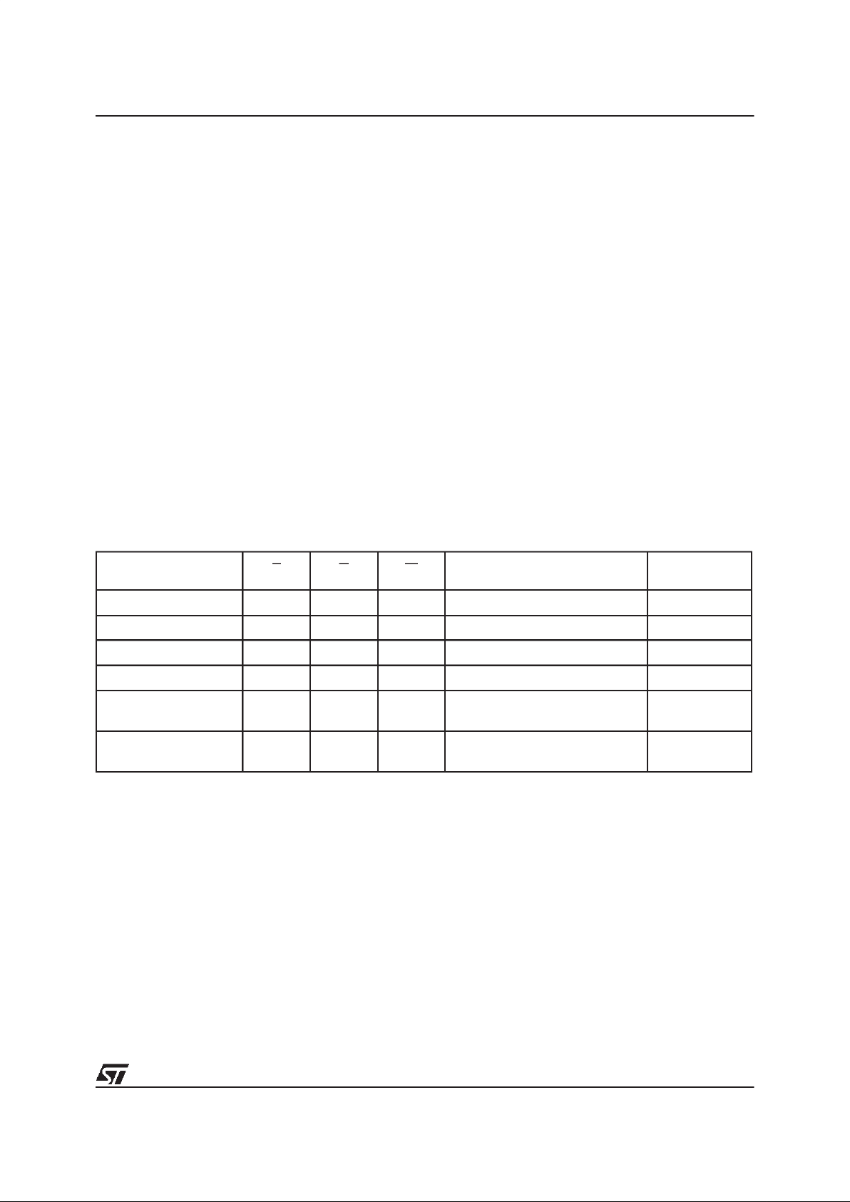
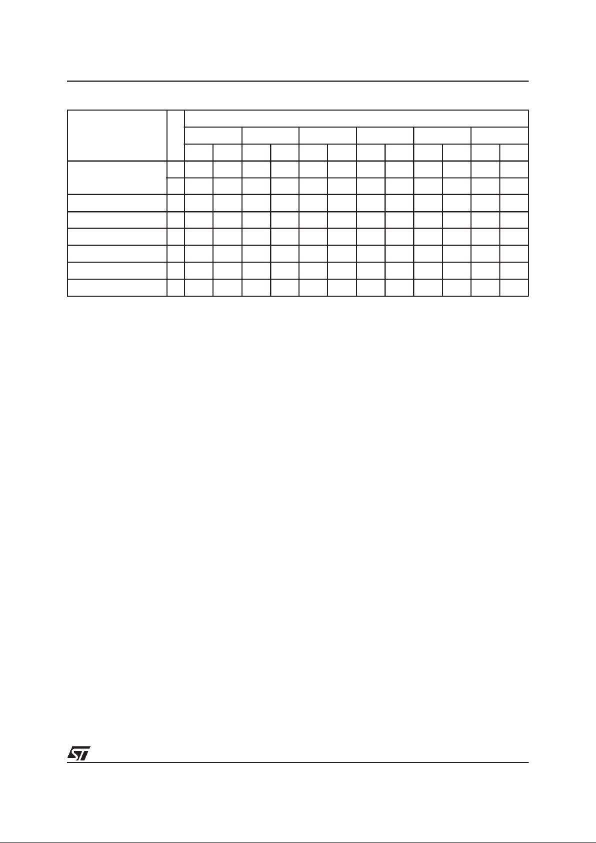
Table 5. Commands
Note: X Don’t Care, PA Program Address, PD Program Data, BA Any address in the Block.
All values in the table are in hexadecimal.
The Command Interface only uses address bits A0-A10 to verify the commands, the upper address bits are Don’t Care.
Read/Reset. After a Read/Reset command, read the memory as normal until another command is issued.
Auto Select. After an Auto Select command, read Manufacturer ID, Device ID or Block Protection Status.
Program, Chip Erase, Block Erase. After these commands read the Status Register until the Program/Erase Controller completes and the
memory returns to Read Mode. Add additional Blocks during Block Erase Command with additional Bus WriteOperations until the Timeout
Bit is set.
Erase Suspend. After the Erase Suspend command read non-erasing memory blocks as normal, issue AutoSelect and Program commands
on non-erasing blocks as normal.
Erase Resume. After the Erase Resume command the suspended Erase operation resumes, read the Status Register until the Program/
Erase Controller completes and the memory returns to Read Mode.
Command
Length
Bus Write Operations
1st 2nd 3rd 4th 5th 6th
Addr Data Addr Data Addr Data Addr Data Addr Data Addr Data
Read/Reset
1X F0
3 555 AA 2AA 55 X F0
Auto Select 3 555 AA 2AA 55 555 90
Program 4 555 AA 2AA 55 555 A0 PA PD
Chip Erase 6 555 AA 2AA 55 555 80 555 AA 2AA 55 555 10
Block Erase 6+ 555 AA 2AA 55 555 80 555 AA 2AA 55 BA 30
Erase Suspend 1 X B0
Erase Resume 1 X 30
Chip Erase Command. The Chip Erase command can beused to erasethe entire chip. Six Bus
Write operations are required to issue the Chip
Erase Command and start the Program/Erase
Controller.
If any blocks are protected then these are ignored
and all the other blocks are erased. If all of the
blocks are protected the ChipErase operation appears tostart but willterminate within about 100µs,
leaving the data unchanged. No error condition is
given when protected blocks are ignored.
During the erase operation the memory will ignore
all commands. It is not possible to issue any command to abort the operation. Typical chip erase
times are given in Table 6. All Bus Read operations during the Chip Erase operation will output
the Status Register on the Data Inputs/Outputs.
See the section on the Status Register for more
details.
After the Chip Erase operation has completed the
memory will return to the Read Mode, unless an
error has occurred. When an error occurs the
memory will continue to output the Status Register. A Read/Reset command must be issued to reset the error condition and return to Read Mode.
TheChip Erase Command sets allof the bits inunprotected blocks of the memory to ’1’. All previous
data is lost.
 Loading...