

32 Mbit (4Mb x8 or 2Mb x16, Dual Bank 16:16, Boot Block)
FEATURES SUMMARY
■ SUPPLY VOLTAGE
–V
–V
■ ACCESS TIME: 70, 90ns
■ PROGRAMMING TIME
– 10µs per Byte/Word typical
– Double Word/ Quadruple Byte Program
■ MEMORY BLOCKS
– Dual Bank Memory Array: 16Mbit+16Mbit
– Parameter Blocks (Top or Bott o m Locati o n)
■ DUAL OPERATIONS
– Read in one bank while Program or Erase in
■ ERASE SUSPEND and RESUME MODES
– Read and Program another Block during
■ UNLOCK BYPASS PROGRAM COMMAND
– Faster Production/Batch Programm ing
■ V
PP
PROTECT
■ TEMPORARY BLOCK UNPROTECTION
MODE
■ COMMON FLASH INTERFACE
– 64 bit Security Code
■ EXTENDED MEMORY BL OCK
– Extra block used as security block or to store
■ LOW POWER CONSUMPTION
– Standby and Automatic Standby
■ 100,000 PROGRAM/ER ASE CYCL ES per
BLOCK
■ ELECTRONIC SIGNATURE
– Manufacturer Code: 0020h
– Top Device Code M29DW324DT: 225Ch
– Bottom Device Code M29DW324DB: 225Dh
2.7V to 3.6V for Program, Erase and
CC =
Read
=12V for Fast Program (optional)
PP
other
Erase Suspend
/WP PIN for FAST PROGRAM and W R IT E
additional information
M29DW324DT
M29DW324DB
3V Supply Fl ash Mem ory
Figure 1. Packages
TSOP48 (N)
12 x 20mm
FBGA
TFBGA63 (ZA)
7 x 11mm
FBGA
TFBGA48 (ZE)
6 x 8mm
1/49June 2003

M29DW324DT, M29DW324DB
TABLE OF CONTENTS
SUMMARY DESCRIPTION. . . . . . . . . . . . . . . . . . . . . . . . . . . . . . . . . . . . . . . . . . . . . . . . . . . . . . . . . . . 5
Figure 2. Logic Diagram . . . . . . . . . . . . . . . . . . . . . . . . . . . . . . . . . . . . . . . . . . . . . . . . . . . . . . . . . . 5
Table 1. Signal Names . . . . . . . . . . . . . . . . . . . . . . . . . . . . . . . . . . . . . . . . . . . . . . . . . . . . . . . . . . . 5
Figure 3. TSOP Connections . . . . . . . . . . . . . . . . . . . . . . . . . . . . . . . . . . . . . . . . . . . . . . . . . . . . . . . 6
Figure 4. TFBGA63 Connections (Top view through package). . . . . . . . . . . . . . . . . . . . . . . . . . . . . 7
Figure 5. TFBGA48 Connections (Top view through package). . . . . . . . . . . . . . . . . . . . . . . . . . . . . 8
Table 2. Bank Architecture . . . . . . . . . . . . . . . . . . . . . . . . . . . . . . . . . . . . . . . . . . . . . . . . . . . . . . . . 8
Figure 6. Block Addresses (x8). . . . . . . . . . . . . . . . . . . . . . . . . . . . . . . . . . . . . . . . . . . . . . . . . . . . . 9
Figure 7. Block Addresses (x16). . . . . . . . . . . . . . . . . . . . . . . . . . . . . . . . . . . . . . . . . . . . . . . . . . . 10
SIGNAL DESCRIPTIONS . . . . . . . . . . . . . . . . . . . . . . . . . . . . . . . . . . . . . . . . . . . . . . . . . . . . . . . . . . . 11
Address Inputs (A0-A20). . . . . . . . . . . . . . . . . . . . . . . . . . . . . . . . . . . . . . . . . . . . . . . . . . . . . . . . . 11
Data Inputs/Outputs (DQ0-DQ7). . . . . . . . . . . . . . . . . . . . . . . . . . . . . . . . . . . . . . . . . . . . . . . . . . . 11
Data Inputs/Outputs (DQ8-DQ14 ). . . . . . . . . . . . . . . . . . . . . . . . . . . . . . . . . . . . . . . . . . . . . . . . . .11
Data Input/Output or Address Input (DQ15A–1). . . . . . . . . . . . . . . . . . . . . . . . . . . . . . . . . . . . . . . . 11
Chip Enable (E). . . . . . . . . . . . . . . . . . . . . . . . . . . . . . . . . . . . . . . . . . . . . . . . . . . . . . . . . . . . . . . . 11
Output Enable (G). . . . . . . . . . . . . . . . . . . . . . . . . . . . . . . . . . . . . . . . . . . . . . . . . . . . . . . . . . . . . . 11
Write Enable (W). . . . . . . . . . . . . . . . . . . . . . . . . . . . . . . . . . . . . . . . . . . . . . . . . . . . . . . . . . . . . . . 11
V
Write Protect (V
PP/
Reset/Block Temporary Unprotect (RP).. . . . . . . . . . . . . . . . . . . . . . . . . . . . . . . . . . . . . . . . . . . . .11
Ready/Busy Output (RB). . . . . . . . . . . . . . . . . . . . . . . . . . . . . . . . . . . . . . . . . . . . . . . . . . . . . . . . . 1 1
Byte/Word Organization Select (BYTE). . . . . . . . . . . . . . . . . . . . . . . . . . . . . . . . . . . . . . . . . . . . . . 12
V
Supply Voltage (2.7V to 3.6V).. . . . . . . . . . . . . . . . . . . . . . . . . . . . . . . . . . . . . . . . . . . . . . . . .12
CC
Ground. . . . . . . . . . . . . . . . . . . . . . . . . . . . . . . . . . . . . . . . . . . . . . . . . . . . . . . . . . . . . . . . . . . 12
V
SS
WP). . . . . . . . . . . . . . . . . . . . . . . . . . . . . . . . . . . . . . . . . . . . . . . . . . . . . . . 11
PP/
BUS OPERATIONS. . . . . . . . . . . . . . . . . . . . . . . . . . . . . . . . . . . . . . . . . . . . . . . . . . . . . . . . . . . . . . . . 13
Bus Read. . . . . . . . . . . . . . . . . . . . . . . . . . . . . . . . . . . . . . . . . . . . . . . . . . . . . . . . . . . . . . . . . . . . . 13
Bus Write. . . . . . . . . . . . . . . . . . . . . . . . . . . . . . . . . . . . . . . . . . . . . . . . . . . . . . . . . . . . . . . . . . . . . 13
Output Disable. . . . . . . . . . . . . . . . . . . . . . . . . . . . . . . . . . . . . . . . . . . . . . . . . . . . . . . . . . . . . . . . . 13
Standby. . . . . . . . . . . . . . . . . . . . . . . . . . . . . . . . . . . . . . . . . . . . . . . . . . . . . . . . . . . . . . . . . . . . . . 13
Automatic Standby. . . . . . . . . . . . . . . . . . . . . . . . . . . . . . . . . . . . . . . . . . . . . . . . . . . . . . . . . . . . . . 13
Special Bus Operations . . . . . . . . . . . . . . . . . . . . . . . . . . . . . . . . . . . . . . . . . . . . . . . . . . . . . . . . 1 3
Electronic Signature. . . . . . . . . . . . . . . . . . . . . . . . . . . . . . . . . . . . . . . . . . . . . . . . . . . . . . . . . . . . . 13
Block Protect and Chip Unprotect. . . . . . . . . . . . . . . . . . . . . . . . . . . . . . . . . . . . . . . . . . . . . . . . . . 13
Block Protect and Chip Unprotect. . . . . . . . . . . . . . . . . . . . . . . . . . . . . . . . . . . . . . . . . . . . . . . . . . 13
Table 3. Bus Operations, BYTE = V
Table 4. Bus Operations, BYTE = V
. . . . . . . . . . . . . . . . . . . . . . . . . . . . . . . . . . . . . . . . . . . . . . . 14
IL
. . . . . . . . . . . . . . . . . . . . . . . . . . . . . . . . . . . . . . . . . . . . . . . 14
IH
COMMAND INTERFACE . . . . . . . . . . . . . . . . . . . . . . . . . . . . . . . . . . . . . . . . . . . . . . . . . . . . . . . . . . . 15
Read/Reset Command . . . . . . . . . . . . . . . . . . . . . . . . . . . . . . . . . . . . . . . . . . . . . . . . . . . . . . . . . . 15
Auto Select Command. . . . . . . . . . . . . . . . . . . . . . . . . . . . . . . . . . . . . . . . . . . . . . . . . . . . . . . . . . . 15
Program Command. . . . . . . . . . . . . . . . . . . . . . . . . . . . . . . . . . . . . . . . . . . . . . . . . . . . . . . . . . . . . 15
Fast Program Commands . . . . . . . . . . . . . . . . . . . . . . . . . . . . . . . . . . . . . . . . . . . . . . . . . . . . . . . . 16
2/49

M29DW324DT, M29DW324DB
Quadruple Byte Program Command. . . . . . . . . . . . . . . . . . . . . . . . . . . . . . . . . . . . . . . . . . . . . . . . 16
Double Word Program Command. . . . . . . . . . . . . . . . . . . . . . . . . . . . . . . . . . . . . . . . . . . . . . . . . . 16
Unlock Bypass Command. . . . . . . . . . . . . . . . . . . . . . . . . . . . . . . . . . . . . . . . . . . . . . . . . . . . . . . . 16
Unlock Bypass Program Command. . . . . . . . . . . . . . . . . . . . . . . . . . . . . . . . . . . . . . . . . . . . . . . . . 16
Unlock Bypass Reset Command. . . . . . . . . . . . . . . . . . . . . . . . . . . . . . . . . . . . . . . . . . . . . . . . . . .16
Chip Erase Command. . . . . . . . . . . . . . . . . . . . . . . . . . . . . . . . . . . . . . . . . . . . . . . . . . . . . . . . . . . 16
Block Erase Command.. . . . . . . . . . . . . . . . . . . . . . . . . . . . . . . . . . . . . . . . . . . . . . . . . . . . . . . . . . 17
Erase Suspend Comma nd. . . . . . . . . . . . . . . . . . . . . . . . . . . . . . . . . . . . . . . . . . . . . . . . . . . . . . . . 17
Erase Resume Command. . . . . . . . . . . . . . . . . . . . . . . . . . . . . . . . . . . . . . . . . . . . . . . . . . . . . . . . 17
Enter Extended Block Command . . . . . . . . . . . . . . . . . . . . . . . . . . . . . . . . . . . . . . . . . . . . . . . . . .18
Exit Extended Block Command. . . . . . . . . . . . . . . . . . . . . . . . . . . . . . . . . . . . . . . . . . . . . . . . . . . . 18
Table 5. Commands, 16-bit mode, BYTE = V
Table 6. Commands, 8-bit mode, BYTE = V
Table 7. Program, Erase Times and Program, Erase Endurance Cycles . . . . . . . . . . . . . . . . . . . . 19
STATUS REGISTER. . . . . . . . . . . . . . . . . . . . . . . . . . . . . . . . . . . . . . . . . . . . . . . . . . . . . . . . . . . . . . . 20
Data Polling Bit (DQ7). . . . . . . . . . . . . . . . . . . . . . . . . . . . . . . . . . . . . . . . . . . . . . . . . . . . . . . . . . . 20
Toggle Bit (DQ6).. . . . . . . . . . . . . . . . . . . . . . . . . . . . . . . . . . . . . . . . . . . . . . . . . . . . . . . . . . . . . . . 20
Error Bit (DQ5). . . . . . . . . . . . . . . . . . . . . . . . . . . . . . . . . . . . . . . . . . . . . . . . . . . . . . . . . . . . . . . . . 20
Erase Timer Bit (DQ3). . . . . . . . . . . . . . . . . . . . . . . . . . . . . . . . . . . . . . . . . . . . . . . . . . . . . . . . . . . 20
Alternative Toggle Bit (DQ2).. . . . . . . . . . . . . . . . . . . . . . . . . . . . . . . . . . . . . . . . . . . . . . . . . . . . . . 20
Table 8. Status Register Bits. . . . . . . . . . . . . . . . . . . . . . . . . . . . . . . . . . . . . . . . . . . . . . . . . . . . . . 21
Figure 8. Data Polling Flowchart . . . . . . . . . . . . . . . . . . . . . . . . . . . . . . . . . . . . . . . . . . . . . . . . . . . 21
Figure 9. Data Toggle Flowchart. . . . . . . . . . . . . . . . . . . . . . . . . . . . . . . . . . . . . . . . . . . . . . . . . . . 2 1
. . . . . . . . . . . . . . . . . . . . . . . . . . . . . . . . . . . . . . .18
IH
. . . . . . . . . . . . . . . . . . . . . . . . . . . . . . . . . . . . . . . . . 19
IL
MAXIMUM RATING. . . . . . . . . . . . . . . . . . . . . . . . . . . . . . . . . . . . . . . . . . . . . . . . . . . . . . . . . . . . . . . . 22
Table 9. Absolute Maximum Ratings. . . . . . . . . . . . . . . . . . . . . . . . . . . . . . . . . . . . . . . . . . . . . . . .22
DC and AC PARAMETERS . . . . . . . . . . . . . . . . . . . . . . . . . . . . . . . . . . . . . . . . . . . . . . . . . . . . . . . . . 23
Table 10. Operating and AC Measurement Conditions. . . . . . . . . . . . . . . . . . . . . . . . . . . . . . . . . . 23
Figure 10. AC Measurement I/O Waveform . . . . . . . . . . . . . . . . . . . . . . . . . . . . . . . . . . . . . . . . . .23
Figure 11. AC Measurement Load Circuit. . . . . . . . . . . . . . . . . . . . . . . . . . . . . . . . . . . . . . . . . . . . 23
Table 11. Device Capacitance . . . . . . . . . . . . . . . . . . . . . . . . . . . . . . . . . . . . . . . . . . . . . . . . . . . . . 23
Table 12. DC Characteristics. . . . . . . . . . . . . . . . . . . . . . . . . . . . . . . . . . . . . . . . . . . . . . . . . . . . . . 24
Figure 12. Read Mode AC Waveforms . . . . . . . . . . . . . . . . . . . . . . . . . . . . . . . . . . . . . . . . . . . . . . 25
Table 13. Read AC Characteristics . . . . . . . . . . . . . . . . . . . . . . . . . . . . . . . . . . . . . . . . . . . . . . . . . 25
Figure 13. Write AC Waveforms, Write Enable Controlled . . . . . . . . . . . . . . . . . . . . . . . . . . . . . . . 26
Table 14. Write AC Characteristics, Write Enable Controlled . . . . . . . . . . . . . . . . . . . . . . . . . . . . . 26
Figure 14. Write AC Waveforms, Chip Enable Controlled . . . . . . . . . . . . . . . . . . . . . . . . . . . . . . . .27
Table 15. Write AC Characteristics, Chip Enable Controlled . . . . . . . . . . . . . . . . . . . . . . . . . . . . . 27
Figure 15. Reset/Block Temporary Unprotect AC Waveforms . . . . . . . . . . . . . . . . . . . . . . . . . . . . 28
Table 16. Reset/Block Temporary Unprotect AC Characteristi cs . . . . . . . . . . . . . . . . . . . . . . . . . . 28
Figure 16. Accelerated Program Timing Waveforms. . . . . . . . . . . . . . . . . . . . . . . . . . . . . . . . . . . . 28
PACKAGE MECHANICAL . . . . . . . . . . . . . . . . . . . . . . . . . . . . . . . . . . . . . . . . . . . . . . . . . . . . . . . . . . 29
Figure 17. 48 Lead Plastic Thin Small Outline, 12x20 mm, Bottom View Package Outline . . . . . . 29
3/49

M29DW324DT, M29DW324DB
Table 17. 48 Lead Plastic Thin Small Outline, 12x20 mm, Package Mechanical Data . . . . . . . . . . 29
Figure 18. TFBGA63 7x11mm - 6x8 Ball Array, 0.8mm Pitch, Bottom View Package Outli ne . . . . 30
Table 18. TFBGA63 7x11mm - 6x8 Ball Array, 0.8mm Pitch, Package Mechanical Data. . . . . . . . 30
Figure 19. TFBGA48 6x8mm - 6x8 Ball Array, 0.8mm Pitch, Bottom View Package Outlin e . . . . . 31
Table 19. TFBGA48 6x8mm - 6x8 Ball Array, 0.8mm Pitch, Package Mechanical Data. . . . . . . . . 31
PART NUMBERING . . . . . . . . . . . . . . . . . . . . . . . . . . . . . . . . . . . . . . . . . . . . . . . . . . . . . . . . . . . . . . . 32
Table 20. Ordering Information Scheme . . . . . . . . . . . . . . . . . . . . . . . . . . . . . . . . . . . . . . . . . . . . .32
APPENDIX A. BLOCK ADDRESSES. . . . . . . . . . . . . . . . . . . . . . . . . . . . . . . . . . . . . . . . . . . . . . . . . . 33
Table 21. Top Boot Block Addresses, M29DW324DT . . . . . . . . . . . . . . . . . . . . . . . . . . . . . . . . . . 33
Table 22. Bottom Boot Block Addresses, M29DW324DB. . . . . . . . . . . . . . . . . . . . . . . . . . . . . . . . 36
APPENDIX B. COMMON FLASH INT ERFACE (CFI) . . . . . . . . . . . . . . . . . . . . . . . . . . . . . . . . . . . . . 39
Table 23. Query Structure Overview. . . . . . . . . . . . . . . . . . . . . . . . . . . . . . . . . . . . . . . . . . . . . . . .39
Table 24. CFI Query Identification String . . . . . . . . . . . . . . . . . . . . . . . . . . . . . . . . . . . . . . . . . . . .39
Table 25. CFI Query System Interface Information. . . . . . . . . . . . . . . . . . . . . . . . . . . . . . . . . . . . . 40
Table 26. Device Geometry Definition. . . . . . . . . . . . . . . . . . . . . . . . . . . . . . . . . . . . . . . . . . . . . . .40
Table 27. Primary Algorithm-Specific Extended Query Table . . . . . . . . . . . . . . . . . . . . . . . . . . . . . 41
Table 28. Security Code Area . . . . . . . . . . . . . . . . . . . . . . . . . . . . . . . . . . . . . . . . . . . . . . . . . . . . . 41
APPENDIX C. EXTENDED MEMORY BLOCK . . . . . . . . . . . . . . . . . . . . . . . . . . . . . . . . . . . . . . . . . . 42
Factory Locked Extended Block . . . . . . . . . . . . . . . . . . . . . . . . . . . . . . . . . . . . . . . . . . . . . . . . . 42
Customer Lockable Extended Block. . . . . . . . . . . . . . . . . . . . . . . . . . . . . . . . . . . . . . . . . . . . . . 42
Table 29. Extended Block Address and Data . . . . . . . . . . . . . . . . . . . . . . . . . . . . . . . . . . . . . . . . . 42
APPENDIX D. BLOCK PROTECTION . . . . . . . . . . . . . . . . . . . . . . . . . . . . . . . . . . . . . . . . . . . . . . . . . 43
Programmer Technique . . . . . . . . . . . . . . . . . . . . . . . . . . . . . . . . . . . . . . . . . . . . . . . . . . . . . . . . 43
In-System Technique . . . . . . . . . . . . . . . . . . . . . . . . . . . . . . . . . . . . . . . . . . . . . . . . . . . . . . . . . . 43
Table 30. Programmer Technique Bus Operations, BYTE = V
or VIL . . . . . . . . . . . . . . . . . . . . .43
IH
Figure 20. Programmer Equipment Group Protect Flowchart. . . . . . . . . . . . . . . . . . . . . . . . . . . . . 44
Figure 21. Programmer Equipment Chip Unprotect Flowchart . . . . . . . . . . . . . . . . . . . . . . . . . . . . 45
Figure 22. In-System Equipment G roup Protect Flowchart. . . . . . . . . . . . . . . . . . . . . . . . . . . . . . . 46
Figure 23. In-System Equipment Chip Unprotect Flowchart . . . . . . . . . . . . . . . . . . . . . . . . . . . . . . 47
REVISION HISTORY. . . . . . . . . . . . . . . . . . . . . . . . . . . . . . . . . . . . . . . . . . . . . . . . . . . . . . . . . . . . . . . 48
Table 31. Document Revision History . . . . . . . . . . . . . . . . . . . . . . . . . . . . . . . . . . . . . . . . . . . . . . .48
4/49
SUMMARY DESCRIPTION
The M29DW324D is a 32 Mbit (4Mb x8 or 2Mb
x16) non-volatile memory that can be read, erased
and reprogrammed. These operations can be performed using a single low voltage (2.7 to 3.6V)
supply. On power-up the memory d efaults to its
Read mode where it can be read in the same way
as a ROM or EPROM.
The device features an asymmet rical block architecture. The M29DW324D has an array of 8 parameter and 63 main blocks and is divided into two
Banks, A and B, providing Dual Bank operations.
While programming or erasing in Bank A, read operations are possible in Bank B and vice versa.
Only one bank at a time is allowed to be in program or erase mode. The bank architecture is
summarized in Table 2. M29DW324DT locates the
Parameter Blocks at the top of the memory address space while the M29DW324DB locates the
Parameter Blocks starting from the bottom.
M29DW324D h as an extra 32 KWord (x16 mode)
or 64 KByte (x8 mode) block, the Extended Block,
that can be accessed using a dedicated command. The Extended Block can be protected and
so is useful for storing security information. How-
M29DW324DT, M29DW324DB
ever the protection is irreversible, once protected
the protection cannot be undone.
Each block can be erased indep endently so it is
possible to preserve valid dat a while old data is
erased. The blocks can be protected to prevent
accidental Program or Erase commands from
modifying the memory. Program and E rase commands are written to the Command Interface of
the memory. An on-chip Program/Erase Controller
simplifies the process of prog ramming or eras ing
the memory by taking care of all of the special operations that are required to update the memory
contents. The end of a program or erase operation
can be detected and any error conditions identified. The command set required to control the
memory is consistent with JEDEC standards.
Chip Enable, Output Enable and Write Enable signals control the bus operation of the memory.
They allow simple conne ction to most m icroprocessors, often without additional logic.
The memory is offered in TSOP48 (12x20mm),
TFBGA63 (7x11mm, 0.8mm pitch) and TFBGA48
(6x8mm, 0.8mm pitch) packages. The memory is
supplied with all the bi t s erased (set t o ’1’).
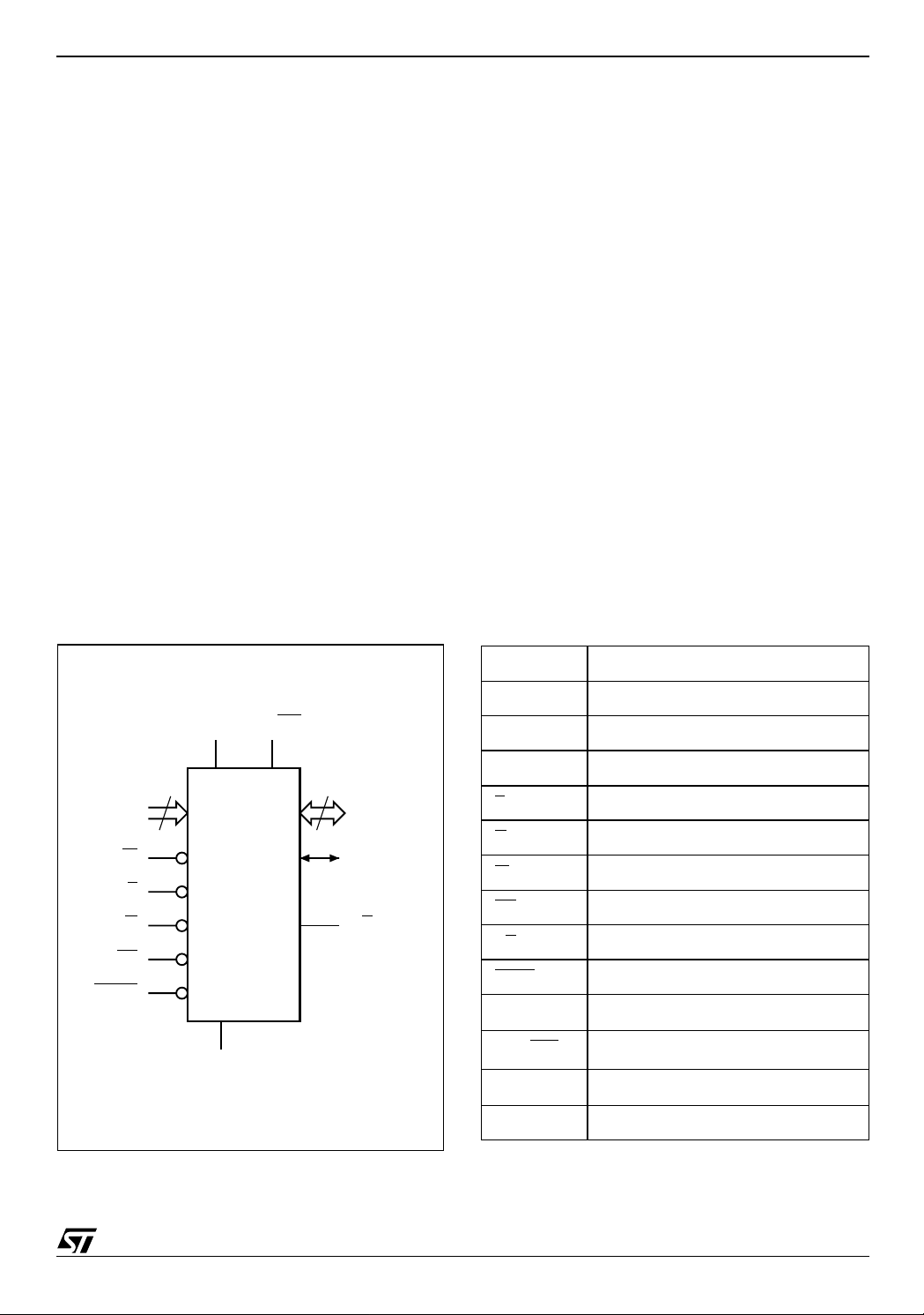
Figure 2. Logic Diagram Table 1. Signal Names
A0-A20 Address Inputs
DQ0-DQ7 Data Inputs/Outputs
VPP/WP
V
A0-A20
W
RP
BYTE
CC
21
E
G
M29DW324DT
M29DW324DB
V
SS
15
DQ0-DQ14
DQ15A–1
RB
AI06867B
DQ8-DQ14 Data Inputs/Outputs
DQ15A–1 Data Input/Output or Address Input
E
G
W
RP
RB
BYTE
V
CC
VPP/WP
V
SS
NC Not Connected Internally
Chip Enable
Output Enable
Write Enable
Reset/Block Temporary Unprotect
Ready/Busy Output
Byte/Word Organization Select
Supply Voltage
VPP/Write Protect
Ground
5/49
M29DW324DT, M29DW324DB
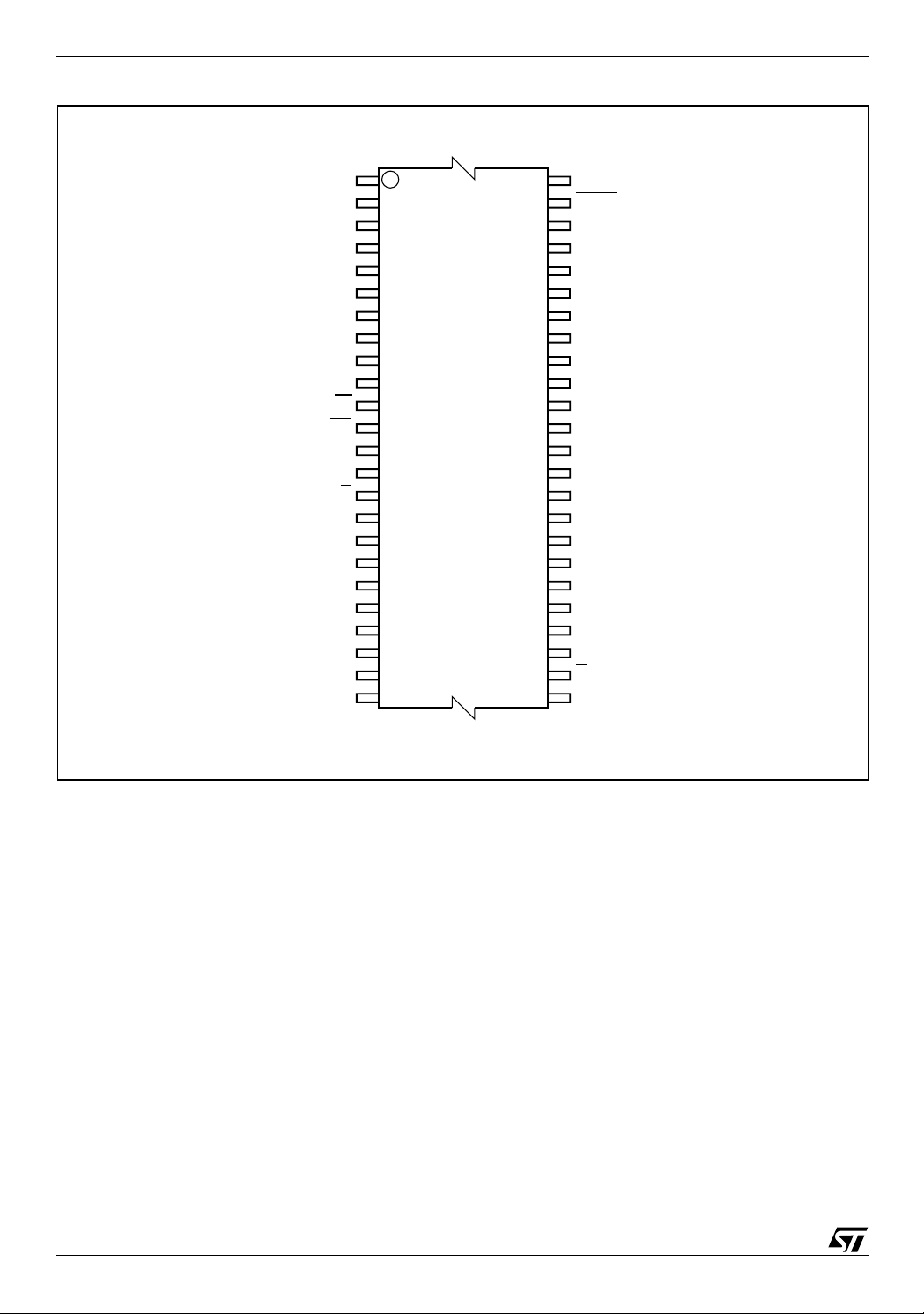
Figure 3. TSOP Connections
A15
1
48
A14
A13
A12
A11
A10 DQ14
A9
A8
A19
A20
M29DW324DT
M29DW324DB
W
RP
NC
12
13
37
36
VPP/WP
RB
A18
A17
A7
A6
A5
A4
A3
A2
A1
24 25
A16
BYTE
V
SS
DQ15A–1
DQ7
DQ6
DQ13
DQ5
DQ12
DQ4
V
CC
DQ11
DQ3
DQ10
DQ2
DQ9
DQ1
DQ8
DQ0
G
V
SS
E
A0
6/49
AI06805
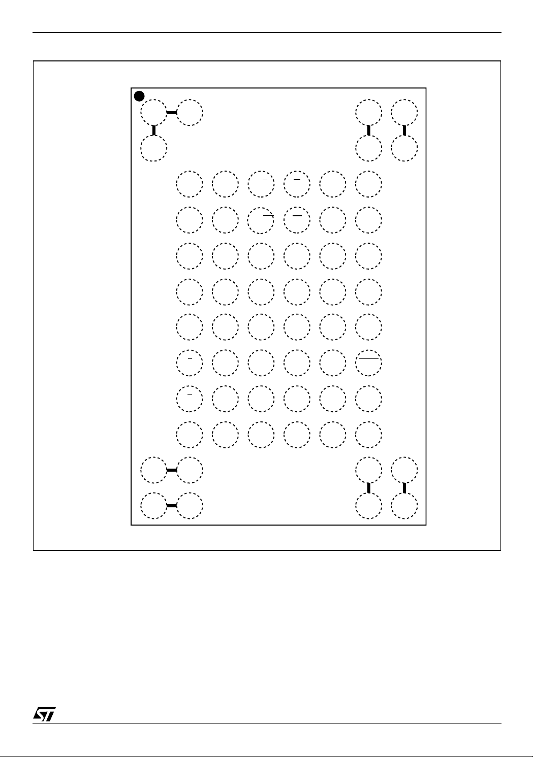
Figure 4. TFBGA63 Conn ections (Top view through packa ge)
M29DW324DT, M29DW324DB
654321
A
B
NC
NC
(1)
(1)
C
D
E
F
G
H
NC
A3
A4
A2
A1
A0
(1)
A7
A17
A6
RB
V
/
PP
A18
A5 A20
DQ0
E
DQ8
DQ2
DQ10
WP
W
RP
NC
A19
DQ5
DQ12
A9
A8
A10
A11
DQ7
DQ14
NC
NC
A13
A12
A14
A15
A16
BYTE
(1)
(1)
NC
NC
87
(1)
(1)
J
K
L
NC
M
NC
G
V
SS
(1)
NC
(1)
NC
DQ9
DQ1
(1)
(1)
DQ11
DQ3
V
CC
DQ4
Note: 1. Balls are shorted together via the substrate but not connecte d to the die.
DQ13
DQ6
DQ15
A–1
V
SS
NC
NC
NC
NC
(1)
(1)
AI05525B
(1)
(1)
7/49
M29DW324DT, M29DW324DB
Figure 5. TFBGA48 Connections (Top view through package)
654321
V
PP
A18
DQ2
DQ10
DQ11
DQ3
RB
/WP
A
B
C
D
E
F
G
H
A3
A4
A2
A1
A0
E
G
V
SS
A7
A17
A6
A5 A20
DQ0
DQ8
DQ9
DQ1
W
RP
NC
A19
DQ5
DQ12
V
CC
DQ4
A9
A8
A10
A11
DQ7
DQ14
DQ13
DQ6
A13
A12
A14
A15
A16
BYTE
DQ15
A–1
V
SS
Table 2. Bank Architecture
Bank Bank Size
A 16 Mbit 8 8KByte/ 4 KWord 31 64KByte/ 32 KWord
B 16 Mbit — — 32 64KByte/ 32 KWord
Parameter Blocks Main Blocks
No. of
Blocks
Block Size No. of Blocks Block Size
AI08084
8/49
Figure 6. Block Addresses (x8)
M29DW324DT, M29DW324DB
Bank B
Bank A
Top Boot Block (x8)
Address lines A20-A0, DQ15A-1
000000h
00FFFFh
1F0000h
1FFFFFh
200000h
20FFFFh
3E0000h
3EFFFFh
3F0000h
3F1FFFh
64 KByte or
32 KWord
64 KByte or
32 KWord
64 KByte or
32 KWord
64 KByte or
32 KWord
8 KByte or
4 KWord
Total of 32
Main Blocks
Total of 31
Main Blocks
Total of 8
Parameter
(1)
Blocks
Bank A
Bank B
Bottom Boot Block (x8)
Address lines A20-A0, DQ15A-1
000000h
001FFFh
00E000h
00FFFFh
010000h
01FFFFh
1F0000h
1FFFFFh
200000h
20FFFFh
8 KByte or
4 KWord
8 KByte or
4 KWord
64 KByte or
32 KWord
64 KByte or
32 KWord
64 KByte or
32 KWord
Total of 8
Parameter
(1)
Blocks
Total of 31
Main Blocks
Total of 32
Main Blocks
3FE000h
3FFFFFh
Note: 1. Used as Extended Block Addre ss es in Exten ded Block mode.
2. Also see Appendix A, Tabl es 21 and 22 for a full l i st i ng of the Block Addresses .
8 KByte or
4 KWord
3F0000h
3FFFFFh
64 KByte or
32 KWord
AI06803
9/49
M29DW324DT, M29DW324DB
Figure 7. Block Addresses (x16)
Bank B
Bank A
000000h
007FFFh
0F8000h
0FFFFFh
100000h
107FFFh
1F0000h
1F7FFFh
1F8000h
1F8FFFh
Top Boot Block (x16)
Address lines A20-A0
64 KByte or
32 KWord
64 KByte or
32 KWord
64 KByte or
32 KWord
64 KByte or
32 KWord
8 KByte or
4 KWord
Total of 32
Main Blocks
Total of 31
Main Blocks
Total of 8
Parameter
(1)
Blocks
Bank A
Bank B
000000h
000FFFh
007000h
007FFFh
008000h
00FFFFh
0F8000h
0FFFFFh
100000h
107FFFh
Bottom Boot Block (x16)
Address lines A20-A0
8 KByte or
4 KWord
8 KByte or
4 KWord
64 KByte or
32 KWord
64 KByte or
32 KWord
64 KByte or
32 KWord
Total of 8
Parameter
(1)
Blocks
Total of 31
Main Blocks
Total of 32
Main Blocks
1FF000h
1FFFFFh
Note: 1. Used as Extended Block Addre ss es in Exten ded Block mode.
2. Also see Appendix A, Tables 21 and 22 for a full listi ng of the Block Addresses.
8 KByte or
4 KWord
1F8000h
1FFFFFh
64 KByte or
32 KWord
AI05555
10/49

SIGNAL DESCRIPTIONS
See Figure 2, Logic Diagram, and Table 1, Sign al
Names, for a brief overview of the signals connected to this device.
Address Inputs (A0-A20). The Address Inputs select the cells i n the memory array to a ccess during Bus Read operations. During Bus Write operations they control the commands sent to the Command Interface of the Program/Erase Controller.
Data Inputs/Outputs (DQ0-DQ7). The Data I/O outputs the data stored at the selected address during a Bus Read operation. During Bus Write operations they represent the commands sent to the Command Interface of the Program/Erase Controller.
Data Inputs/Outputs (DQ8-DQ14). The Data I/O outputs the data stored at the selected address during a Bus Read operation when B Y TE V
. When BYTE is Low, VIL, these pins are not
IH
is High,
used and are high impedance. During Bus Write
operations the Command Register does not use
these bits. When reading the Status Register
these bits should be ignored.
Data Input/Output o r Address Input (DQ15A –1).
When BYTE
is High, VIH, this pin behaves as a
Data Input/Output pin (as DQ8-DQ14). When
is Low, VIL, this pin behaves as an address
BYTE
pin; DQ15A–1 Low will select the LSB of the addressed Word, DQ15A–1 High will select the MSB.
Throughout the text consider references to the
Data Input/Output to include this pin when BYTE
is
High and references to the Address Inputs to include this pin when BYTE
is Low except when
stated explicitly otherwise.
Chip Enable (E
). The Chip Enable, E, activates
the memory, allowing Bus Read and Bus Write operations to be performed. When Chip Enable is
High, V
Output Enable (G
, all other pins are ignored.
IH
). The Output Enable, G, con-
trols the Bus Read operation of the memory.
Write Enable (W
). The Write Enable, W, controls
the Bus Write operation of the memory’s Command Interf a c e .
Write Protect (VPP/WP). The VPP/Write
V
PP/
Protect
pin provides two functions. The VPP function allo ws the memory to use an exte rnal high
volt age power suppl y t o reduce the time required
for P rogram operatio ns. This i s achi eved by bypassing the unlock cycles an d/or using the Double Word or Quadruple Byte Program commands.
The Write Protect function provides a hardware
method of protecting the two outermost boot
blocks.
When VPP/Write Protect is L ow , VIL, the memory
protects the two outermost boot blocks; Program
M29DW324DT, M29DW324DB
and Erase operations in these blocks are ignored
while V
at V
When V
reverts to the previous protection status of the two
outerm os t boot bl ock s . Program and Erase operations can now modify the data in these blocks unless the blocks are protected using Block
Protection.
When V
ory automatically enters the Unlock Bypass mode.
When V
mal operation resumes. During Unlock Bypass
Program operations the memory draws I
the pin to supply the programming circuits. See the
description of the Unlock Bypass comm and in the
Command Interface section. The transitions from
V
IH
than t
Never raise V
mode except Read m ode, otherwise the memory
may be left in an indeterminate state.
The V
or unconnected or the device may become unreliable. A 0.1µF capacitor should be connected between the V
Ground pin to decouple the current surges from
the powe r supply. Th e PCB track wi dths must be
sufficient to carry the currents required during
Unlock Bypass Program, I
Reset/Block Temporary Unprotect (RP
Reset/Block Temporary Unprotect pin can be
used to apply a Hardware Reset to the memory or
to temporarily unprotect all Blocks that hav e b een
protected.
Note that i f V
most boot blocks will remain protected even if RP
is at V
A Hardware Reset is achieved by holding Reset/
Block Temporary Unprotect Low, V
t
PLPX
goes High, V
Read and Bus Write operations after t
t
RHEL
Output section, Table 16 and Figure 15, Reset/
Temporary Unprotect AC Characteristics for more
details.
Holding RP
protected Blocks in the memory. Program and
Erase operations on all blocks will be possible.
The transition from V
t
PHPHH
Ready/Busy Output (RB
is an open-drain output that can be used to identify
when the device is performing a Program or Erase
operation. During Program or Erase operations
/Write Protect is Low, even when RP is
PP
.
ID
/Write Protect is High, VIH, the memo r y
PP
/Write Protect is raised to V
PP
/Write Protect returns to VIH or VIL nor-
PP
the mem-
PP
PP
from
to VPP and from VPP to VIH must be slower
, see Figure 16.
VHVPP
/Write Protect to VPP from any
PP
/Write Protect pin must not be left floating
PP
/Write Protect pin and the V
PP
PP
.
SS
). The
/WP is at VIL, then the two ou ter-
PP
.
ID
, for at least
IL
. After Reset/Block Temporary Unprotect
, the memory will be ready for Bus
IH
PHEL
or
, whichever occurs last. See the Ready/Busy
at VID will temporarily unprotect the
to VID must be slower than
IH
.
). The Ready/Busy pin
11/49

M29DW324DT, M29DW324DB
Ready/Busy is Low, VOL. Ready/Busy is high-impedance during Read mode, Auto Select mode
and Erase Suspend mode.
After a Hardware Reset, Bus Read and Bus Write
operations cannot begin until Ready/Busy becomes high-impedance. See Tabl e 16 and Figure
15, Reset/Temporary Unprotect AC Charac teristics .
The use of an open-drain output allows the Ready/
Busy pins from several memories to be connected
to a single pull-up resistor. A Low will then indicate
that one, or more, of the memories is busy.
Byte/Word Organization Select (BYTE
). The
Byte/Word Organization Select pin is used to
switch between the x8 and x16 Bus modes of the
memory. When Byte/Word Organizati on Select is
Low, V
High, V
, the memory is in x8 mode, when it is
IL
, the memory is in x16 mode.
IH
V
Supply Voltage (2.7V to 3.6V). VCC pro-
CC
vides the power supply for all operations (Read,
Program and Erase).
The Command Interface is disabled when the V
CC
Supply Voltage is less than the L ockout Voltage,
V
. This prevents Bus Write operations from ac-
LKO
cidentally damaging the data during power up,
power down and power surges. If the Program/
Erase Controller is programming or erasing during
this time then the operation aborts and the memory contents being altered will be invalid.
A 0.1µF capacitor should be connected between
the V
Supply Voltage pin and the VSS Ground
CC
pin to decouple the current surges from the power
supply. The PCB track widths must be sufficient to
carry the currents required during Program and
Erase operations, I
Ground. VSS is the reference for all voltage
V
SS
measurements. The device f eatu res two V
CC3
.
pins
SS
which must be both connected to the system
ground.
12/49

BUS OPERATIONS
There are five standard bus operations that control
the device. These are Bus Read, Bus Wri te, Output Disable, Standby and Automatic Standby.
The Dual Bank architecture of the M29DW324D
allows read/write operations in Bank A, while read
operations are being executed in Bank B or vice
versa. Write operations are only allowed in one
bank at a time.
See Tables 3 and 4, Bus Operations, for a summary. Typically glitches of less t han 5ns o n Chi p E nable or Write Enable are ignored b y the memory
and do not affect bus operations.
Bus Read. Bus Read operations read from the memory cells, or specific registers in the Command Interface. A valid Bus Read operation involves setting the desired address on the Address Inputs, applying a Low sig nal, V
, to Chip Enable
IL
and Output Enable and keeping Write Enable
High, V
. The Data Inputs/Outputs will output the
IH
value, see Figure 12, Read Mode AC Waveforms,
and Table 13, Read AC Characteristics, for details
of when the output becomes valid.
Bus Write. Bus Write operations write to the Command Interface. A valid Bus Write operation begins by setting the desire d address on t he Address Inputs. The Address Inputs are latched by the Command Interface on the falling edge of Chip Enable or Write Enable, whichever occurs last. The Data Inputs/Outputs a re latched by the Command Interface on the rising edge of Chip Enable or Write Enable, whichever occurs first. Output Enable must remain High, V
, during the whole Bus
IH
Write operation. See Figures 13 and 14, Write AC
Waveforms, and Tables 14 and 15, Write AC
Characteristics, for details of the timing requirements.
Output Disa bl e . The Data Inputs/Outputs are in the high impedance s tate when Output Enable is High, V
Standby. When Chip Enable is High, V
.
IH
, the
IH
memory enters Standby mode and the Data Inputs/Outputs pins are placed in the high-imped-
M29DW324DT, M29DW324DB
ance state. To reduce the S upply Current to the
Standby Supply Current, I
be held within V
± 0.2V. For the Standby current
CC
level see Table 12, DC Characteristics.
During program or erase operations the memory
will continue to use the Program/Erase Supply
Current, I
, for Program or Erase operations un-
CC3
til the operation completes. Automatic Standby. If CMOS levels (V
are used to drive the bus and the bus is inactive for
300ns or more the memory enters Automatic
Standby where the internal Supply Current is reduced to the Standby Supply Current, I
Data Inputs/Outputs will still output data if a Bus
Read operation is in progress.
Special Bus Operations
Additional bus operations can be performed to
read the Electronic Signature and also to apply
and remove Block Protec tion. These bus operations are intended for use by programming equipment and are not usually used in applications.
They require V
to be applied to some pins.
ID
Electronic Signature. The memory has two codes, the manufacturer code and the device code, that can be read to identify the memory. These codes can be read by applying t he signals listed in Tables 3 and 4, Bus Operations.
Block Protect and Chip Unprotect.
blocks can be protected against accidental Program or Erase. The P rotec tion G roups are shown
in Appendix A, Tables 21 and 22, Block Addresses. The whole chip can be unprotected to allow the
data inside the blocks to be changed.
The V
/Write Protect pin ca n be used t o prote ct
PP
the two outermost boot blocks. When V
Protect
is at V
the two outermost boot blocks are
IL
protected an d remain pr otected regardless of t he
Block Protection Status or the Reset/Block Temporary Unprotect pin status.
Block Protect and Chip Unprote ct operations are
described in Appendix D.
, Chip Enable should
CC2
CC
CC2
Groups of
± 0.2V)
. The
/Write
PP
13/49
M29DW324DT, M29DW324DB
Table 3. Bus Operations, BYTE = V
Operation E G W
Bus Read
Bus Write
Output Disable X
Standby
Read Manufacturer
Code
Read Device Code
Extended Memory
Block Verify Code
Note: X = VIL or VIH.
V
V
V
V
V
V
V
IL
IL
IH
IL
IL
IL
IL
V
IH
V
IH
X X X Hi-Z Hi-Z
V
IL
V
IL
V
IL
Table 4. Bus Operations, BYTE = V
Operation E
Bus Read
Bus Write
Output Disable X
Standby
Read Manufacturer
Code
Read Device Code
Extended Memory
Block Verify Code
Note: X = VIL or VIH.
V
V
V
V
V
V
G W
V
IL
IL
IH
IL
IL
IL
IL
V
IH
V
IH
X X X Hi-Z
V
IL
V
IL
V
IL
IL
Address Inputs
DQ15A–1, A0-A20
V
Cell Address Hi-Z Data Output
IH
V
Command Address Hi-Z Data Input
IL
V
X Hi-Z Hi-Z
IH
A0 = VIL, A1 = VIL, A9 = VID,
V
IH
Others V
A0 = VIH, A1 = VIL,
V
IH
A9 = V
A0 = VIH, A1 = VIH, A6 = VIL,
V
IH
A9 = V
IH
or V
IL
IH
, Others VIL or V
ID
, Others VIL or V
ID
DQ14-DQ8 DQ7-DQ0
IH
IH
Address Inputs
A0-A20
V
Cell Address Data Output
IH
V
Command Address Data Input
IL
V
X Hi-Z
IH
A0 = VIL, A1 = VIL, A9 = VID,
V
IH
Others V
A0 = VIH, A1 = VIL, A9 = VID,
V
IH
Others V
A0 = VIH, A1 = VIH, A6 = VIL,
V
IH
A9 = V
or V
IL
IH
or V
IL
IH
, Others VIL or V
ID
IH
Data Inputs/Outputs
Hi-Z 20h
Hi-Z
Hi-Z
5Ch (M29DW324DT)
5Dh (M29DW324DB)
81h (factory locked)
01h (not factory locked)
Data Inputs/Outputs
DQ15A–1, DQ14-DQ0
225Ch (M29DW324DT)
225Dh (M29DW324DB)
81h (factory locked)
01h (not factory locked)
0020h
14/49

COMMAND INTERFACE
All Bus Write operations t o the me mory are in terpreted by the Command Interface. Commands
consist of one or more sequential Bus Write operations. Failure to observe a valid sequence of Bus
Write operations will result in the memory returning to Read mode. The long command sequences
are imposed to maximize data security.
The address used for the commands changes depending on whether the memory is in 16-bit or 8bit mode. See either Table 5, or 6, de pending on
the configuration that is being used, for a summary
of the commands.
Read/Reset Command
The Read/Reset command returns the memory to
its Read mode where it behaves like a ROM or
EPROM. It also resets the errors in the Status
Register. Either one or three Bus Write operations
can be used to issue the Read/Reset command.
The Read/Reset command can be issued, between Bus Write cycles before the start of a program or erase operation, to return the device to
read mode. If the Read/Reset command is issued
during the timeout of a Block erase operation then
the memory will take up to 10µs to abort. During
the abort period no valid data can be read from the
memory. The Read/Reset command will not abort
an Erase operation when issued while in Erase
Suspend.
Auto Select Command
The Auto Select command is used to read the
Manufacturer Code, the Device Code , the Block
Protection Status and the Extended Memory Block
Verify Code. It can be addressed to either Bank.
Three consecutive Bus Write operations are required to issue the A uto Select comm and. The f inal Write cycle must be addressed to one of the
Banks. Once the Auto Select command is issued
Bus Read operations to the B an k where the command was issued output the Auto Select data. Bus
Read operations to the other Bank will output the
contents of the memory array. The memory remains in Auto S elect mode until a Re ad/Reset or
CFI Query command is issued.
In Auto Select mode the Manufac turer Code can
be read using a Bus Read operation with A0 = V
and A1 = VIL and A20 = Bank Addres s. The ot her
address bits may be set to either V
or VIH.
IL
The Device Code can be read using a B us Read
operation with A0 = V
and A1 = VIL and A20 =
IH
Bank Address. The other address bits may be set
to either V
or VIH.
IL
The Block Protecti on St at us of e ac h bl ock can be
read using a Bus Rea d operation with A0 = V
A1 = V
, A20 = Bank Address and A12-A17 spec-
IH
IL
ifying the address of the block inside the Bank.
The other address bits ma y be set t o either V
or
IL
M29DW324DT, M29DW324DB
V
. If the addressed block is protected then 01h is
IH
output on Data Inputs/Outputs DQ0-DQ7, otherwise 00h is output.
Read CFI Query Command
The Read CFI Query Command is used to read
data from the Common Flash Interface (CFI)
Memory Area. This command is valid when the device is in the Read Array mode, or when the device
is in Autose lec ted mode .
One Bus Write cycle is required to issue the Read
CFI Query Command. Once the command is issued subsequent Bus Read ope rations read from
the Common Flash Interface Memory Area.
The Read/Reset command m ust be issued to return the device to the previous mode (the Read Array mode or Autoselected mode). A second Read/
Reset command would be needed if the device is
to be put in the Read Array mode from Autoselected mode.
See Appendix B, Tables 23, 24, 25, 26, 27 and 28
for details on the information contained in the
Common Flash Interface (CFI) memory area.
Program Command
The Program command can be used to program a
value to one address in the memory array at a
time. The command requires four Bus Write operations, the final write operation latches the address and data, and starts the Program/Erase
Controller.
If the address falls in a pro tected block then the
Program command is ignored, the data remains
unchanged. The Status Register is never read and
no error condition is given.
During the program operat ion the memo ry will ignore all commands. I t is n ot poss ible t o iss ue any
command to abort or pause the operation. After
programming has started, Bus Read operations in
the Bank being programmed output the Status
Register content, while Bus Read operations to
the other Bank output the contents of the memory
array. See the section on the Status Register for
more details. Typical program times are g iven in
Table 7.
After the program operation has completed the
IL
memory will return to the Read mode, unle ss an
error has occurred. When an error occurs Bus
Read operations to the Bank where the command
was issued will continue to output the Status Register. A Read/Reset command must be issued t o
reset the error condition and return t o Read mode.
Note that the Program command cannot change a
bit set at ’0’ bac k to ’1’. One of the E rase Com-
,
mands must be used to set all the bits in a block or
in the whole memory from ’0’ to ’1’.
15/49

M29DW324DT, M29DW324DB
Fast Program Commands
There are two Fast Program commands available
to improve the programming throughput, by writing
several adjacent words or bytes in parallel. The
Quadruple Byte Program command is available for
x8 operations, while the Double Word Program
command is available for x16 operations.
Quadruple Byte Program Command. The Quadruple Byte Program command is used to write a page of four adjacent Bytes in parallel. The four bytes must differ only for addresses A0, DQ15A-1. Five bus write cycles are necessary to issue the Quadruple Byte Program command .
■ The first bus cycle sets up the Quadruple Byte
Program Command.
■ The second bus cycle latches the Address and
the Data of the first byte to be written.
■ The third bus cycle latches the Address and the
Data of the second byte to be written.
■ The fourth bus cycle latches the Address and
the Data of the third byte to be written.
■ The fifth bus cycl e latches the Addres s and th e
Data of the fourth byte to be written and starts
the Program/Erase Controller.
Double Word Program Command. The Double Word Program command is used to write a p age of two adjacent words in parallel. Th e two words must differ only for the address A0.
Three bus write cycles are necessary to issue the
Double Word Program command.
■ The first bus cycle sets up the Double Word
Program Command.
■ The second bus cycle latches the Address and
the Data of the first word to be written.
■ The third bus cycle latches the Address and the
Data of the second word to be written and starts
the Program/Erase Controller.
Only one bank can be programmed at any one
time. The other b ank must be in Read mode or
Erase Suspend.
Programming should not be attempted when V
is not at V
PPH
.
PP
After programming has started, Bus Read operations in the Bank being programmed output the
Status Register content, while Bus Read operations to the other B ank outpu t the cont ents of t he
memory ar ray.
After the program operation has completed the
memory will return to the Read mode, unle ss an
error has occurred. When an error occurs Bus
Read operations to the Bank where the command
was issued will continue to output the Status Register. A Read/Reset command must be issued to
reset the error condition and return t o Read mode.
Note that the Fast Program commands cannot
change a bit set at ’0’ back to ’1’. One of the Erase
Commands must be used to set all the bits in a
block or in the whole memory from ’0’ to ’1’.
Typical Program times are given in Tab le 7, Program, Erase Times and Program/Erase Endurance Cycles.
Unlock Bypass Command.
The Unlock Bypass command is used in conjunction with the Unlock Bypass Program command to
program the memory faster than with the standard
program commands. Whe n the cycle time to the
device is long (as with some EPROM programmers) considerable time saving can be m ade by
using these commands. Three Bus Write operations are required to issue the Unlock Bypass
command.
Once the Unlock Bypas s command has bee n issued the bank enters Unlock Bypass mode. The
Unlock Bypass Program command can then be issued to program addresses within the bank, or the
Unlock Bypass Reset command can be issued to
return the bank to Read mode. In Unlock Bypass
mode the memory can be read as if in Read mode.
When V
is applied to the VPP/Write Protect pin
PP
the memory automatically enters the Unlock Bypass mode and the Unlock Bypass Program command can be issued immediately.
Unlock Bypass Program Command.
The Unlock Bypass Program command can be
used to program one address in the memory array
at a time. The command requires two B us Write
operations, the final write operation latches the address and data, and starts the Program/Erase
Controller.
The Program operation using the Unlock Bypass
Program command behaves identically to the Program operation using the Program command. The
operation cannot be aborted, a Bus Read operation to the Bank where the command was issued
outputs the Status Register. See the Program
command for details on the behavior.
Unlock Bypass Reset Command.
The Unlock Bypass Rese t command can be used
to return to Read/Reset mode from Unlock Bypass
Mode. Two Bus Write operations are required to
issue the Unlock Bypass Reset command. Read/
Reset command does not exit from Unlock Bypass
Mode.
Chip Erase Command.
The Chip Erase command can be used to erase
the entire chip. Six Bus Write operations a re required to issue the Chip Erase Command and start
the Program/Erase Controller.
If any blocks are protected then these are ignored
and all the other blocks are erased. If all of the
16/49

M29DW324DT, M29DW324DB
blocks are protect e d th e Chip Erase op erat i on ap-
pears to start but will terminate within about 100µs,
leaving the data unchanged. No error condition is
given when protected blocks are ignored.
During the erase operation the memory will ignore
all commands, including the Erase Suspen d command. It is not possible to i ssue any c ommand t o
abort the operation. Typical chip erase tim es are
given in Table 7. All Bus Read operations during
the Chip Erase operation will output the Status
Register on the Data Inputs/Outputs. See the section on the Status Register for more details.
After the Chip Erase operation has completed t he
memory will return to the Read Mode, unle ss an
error has occurred. When an error occurs the
memory will continue to output the Status Register. A Read/Reset command must be issued to reset the error condition and return to Read Mode.
The Chip Erase Command sets all of the bits in unprotected blocks of the memory to ’1’. All previous
data is lost.
Block Erase Command.
The Block Erase com mand can be used to erase
a list of one or more blocks in a Bank. It sets all of
the bits in the unprotected selected blocks to ’1’.
All previous data in the selected blocks is lost.
Six Bus Write operations are required to select the
first block in the list. Each a dditional block in the
list can be selected by repeating the sixth Bus
Write operation using the address of the additional
block. All blocks must belong to the same Bank; if
a block belonging to th e other B ank is given it will
not be erased. The Block Erase operation starts
the Program/Erase Controller after a t ime-out period of 50µs after the last Bus Write operation.
Once the Pr ogram /Erase Co ntroller st arts it is not
possible to select any more blocks. Each additional block must therefore be selected within 50µs of
the last block. The 50µs timer restarts when an additional block is selected. After the sixth Bus Write
operation a Bus Read ope ration within the same
Bank will output the S ta tus R e gister. Se e the Status Register section for details on how to identify if
the Program/Erase Controller has started the
Block Erase operation.
If any selected blocks are protected then these are
ignored and all the other selected blocks are
erased. If all of the selected blocks are p rotected
the Block Erase operation appears to start but will
terminate within about 100µs, leaving the data unchanged. No error condition is given when protected blocks are ignored.
During the Block Erase operation the me mory wi ll
ignore all commands except the Erase Susp end
command and the Read/Reset command which is
only accepted during the 50µs time-out period.
Typical block erase times are given in Table 7.
After the Erase operation has started all Bus Read
operations to the Bank being erased will output the
Status Register on the Data Inputs/Outputs. See
the section on the Status Register for more details.
After the Block Erase operation has completed the
memory will return to the Read Mode, unle ss an
error has occurred. When an error occurs Bus
Read operations to the Bank where the command
was issued will continue to output the Status Register. A Read/Reset command must be issued t o
reset the error condition and return t o Read mode.
Erase Suspend Command.
The Erase Suspend Command may be used to
temporarily suspend a B lock Eras e operation and
return the memory to Read mode. T he comm and
requires one Bus Write operation.
The Program/Eras e Controlle r will suspend within
the Erase Suspend Latency time of the Erase Suspend Command being issued. Once the Program/
Erase Controller has stopped the mem ory will be
set to Read mode and the E ras e wi ll be s uspended. If the Erase Suspend command is issued during the period when the memory is waiting for an
additional block (before the Program/Er ase Controller starts) then the Erase is suspended immediately and will start immediately when the Erase
Resume Command is issued. It is not possibl e to
select any further blocks to erase after the Erase
Resume.
During Erase Suspend it is possible to Read and
Program cells in blocks that are not being erased;
both Read and Program operations behave as
normal on these blocks. If any attempt is made to
program in a protected block or in the suspended
block then the Program comm and is ignored and
the data remains unchanged. The Status Register
is not read and no error condi tion is given. Reading from blocks that are being erased will output
the Status Register.
It is also possible to issue the Auto Select, Read
CFI Query and Unlock Bypass commands du ring
an Erase Suspend. The Read/Reset command
must be issued to return the device to Read Array
mode before the Resume command will be accepte d.
During Erase Suspend a Bus Read operation to
the Extended Block will output the Extended Block
data.
Erase Resume Command.
The Erase Resume command must be used to restart the Program/Erase Controller after an Erase
Suspend. The device must be in Read Array mode
before the Resume command will be accepted. An
erase can be suspe nded and resumed mo re than
once.
17/49

M29DW324DT, M29DW324DB
Enter Extended Block Command
The M29DW324D has an extra 64KByte block
(Extended Block) that can only be accessed using
the Enter Extended Block command. Three Bus
write cycles are required to issue the Extended
Block command. Once the command has been issued the device enters Extended Block mode
where all Bus Read or Program operations to the
Boot Block addresses access the Extended Block.
The Extended Block (with the same address as
the boot block) cannot be erased, and can be
treated as one-time prog rammabl e (OTP) m emory. In Extended Block mode the Boot Blocks are
not accessible. In Extended Block mode dual operations are possible, with the Extended Block
mapped in Bank A. When in Extended Block
mode, Erase Commands in Bank A are not allowed.
Table 5. Commands, 16-bit mode, BYTE
Command
1X F0
Read/Reset
3 555 AA 2AA 55 X F0
1st 2nd 3rd 4th 5th 6th
Length
Addr Data Addr Data Addr Data Addr Data Addr Data Addr Dat a
= V
IH
To exit from the Extended Block mode the Exit Extended Block command must be issued.
The Extended Block can be protected, however
once protected the protection cannot be undone.
Exit Extended Block Com m and.
The Exit Extended Block command is used to exit
from the Extended Block mod e and ret urn the device to Read mode. Four Bus Write operations are
required to issue the command.
Block Protect and Chip Unprotect Commands.
Groups of blocks can be protected against acci-
dental Program or Erase. The Protection Groups
are shown in Appendix A, Tables 21 and 22, Block
Addresses. The whole chip can be unprotected to
allow the data inside the blocks to be changed.
Block Protect and Chip Unprote ct operations are
described in Appendix D.
Bus Write Operations
Auto Select 3 555 AA 2AA 55
Program 4 555 AA 2AA 55 555 A0 PA PD
Double Word Program 3 555 50 PA0 PD0 PA1 PD1
Unlock Bypass 3 555 AA 2AA 55 555 20
Unlock Bypass
Program
Unlock Bypass Reset 2 X 90 X 00
Chip Erase 6 555 AA 2AA 55 555 80 555 AA 2AA 55 555 10
Block Erase 6+ 555 AA 2AA 55 555 80 555 AA 2AA 55 BA 30
Erase Suspend 1 BKA B0
Erase Resume 1 BKA 30
Read CFI Query 1 55 98
Enter Extended Block 3 555 AA 2AA 55 555 88
Exit Extended Block 4 555 AA 2AA 55 555 90 X 00
Note: X Don’t Care, PA Progr am Add re ss , PD Pro g ram Data , BA Any address in t he Bl o ck, BKA Ba n k Ad d re ss . All va lu es in the ta b le are in
hexadecimal.
The Com ma nd In terf ace o nly uses A– 1, A0-A1 0 a nd DQ0-D Q7 to v er ify t he co mm ands ; A1 1-A2 0, DQ8- DQ1 4 and DQ 15 are D on’t
Care. DQ15A–1 is A– 1 when BYTE
2X A0PAPD
is VIL or DQ15 when BYTE is VIH.
(BKA)
555
90
18/49

M29DW324DT, M29DW324DB
Table 6. Commands, 8-bit mode, BYTE = V
IL
Bus Write Operations
Command
1st 2nd 3rd 4th 5th 6th
Length
Add Data Add Data Add Data Add Data Add Data Add Data
1X F0
Read/Reset
3 AAA AA 555 55 X F0
Auto Select 3 AAA AA 555 55
(BKA)
AAA
90
Program 4 AAA AA 555 55 AAA A0 PA PD
Quadruple Byte Program 5 AAA 55 PA0 PD0 PA1 PD1 PA2 PD2 PA3 PD3
Unlock Bypass 3 AAA AA 555 55 AAA 20
Unlock Bypass Program 2 X A0 PA PD
Unlock Bypass Reset 2 X 90 X 00
Chip Erase 6 AAA AA 555 55 AAA 80 AAA AA 555 55 AAA 10
Block Erase 6+ AAA AA 555 55 AAA 80 AAA AA 555 55 BA 30
Erase Suspend 1 BKA B0
Erase Resume 1 BKA 30
Read CFI Query 1 AA 98
Enter Extended Block 3 AAA AA 555 55 AAA 88
Exit Extended Block 4 AAA AA 555 55 AAA 90 X 00
Note: X Do n’ t Care, PA Program Address, PD Program Data, B A Any address in the Block. All values i n the table are in hexadecim al .
The Com ma nd In terf ace o nly us es A –1, A0-A 10 a nd DQ 0-DQ 7 t o ver ify the com man ds; A 11-A 2 0, D Q8-DQ1 4 a nd DQ 15 ar e D on’t
Care. DQ15A–1 is A– 1 when BYTE
is VIL or DQ15 when BYTE is VIH.
Table 7. Program, Erase Times and Progra m, Erase Endu ran ce Cycle s
Parameter Min
Typ
(1, 2)
Chip Erase 40
Block Erase (64 KBytes) 0.8
Erase Suspend Latency time
Program (Byte or Word) 10
Double Word Program (Byte or Word) 10
Chip Program (Byte by Byte) 40
Chip Program (Word by Word) 20
Chip Program (Quadruple Byte or Double Word) 10 100 s
Program/Erase Cycles (per Block) 100,000 cycles
Data Retention 20 years
Note: 1. Typical values me asured at room tempera ture and nomi nal voltages.
2. Sampled, but not 100% tested.
3. Maximum value measu red at worst case conditions for both temperature and V
4. Maximum value measu red at worst case conditions for both temperature and V
after 100,0 0 program/erase cycles.
CC
.
CC
Max
200
6
50
200
200
200
100
(3)
(4)
(3)
(4)
(3)
(3)
(3)
(2)
Unit
µs
µs
µs
s
s
s
s
19/49

M29DW324DT, M29DW324DB
STATUS REGISTER
The M29DW324D has two Status Registers, one
for each bank. The Status Registers provide information on the current or previous Program or
Erase operations executed in each bank. The various bits convey information and errors on the operation. Bus Read operations from any address
within the Bank, always read the Status Register
during Program and Erase operations. It is also
read during Erase Suspend when an address within a block being erased is accessed.
The bits in the Status Register are summarized in
Table 8, Status Register Bits.
Data Polling Bit (DQ7). The Data Polling Bit can be used to identify whether the Program/Erase Controller has successfully completed its operation or if it has responded to an Erase Suspend. The Data Polling Bit is output on DQ7 when the Status Register is read.
During Program operations the Data Polling Bit
outputs the complement of the bit being programmed to DQ7. After successful completion of
the Program operation the memory returns to
Read mode and Bus Read operations from the address just programmed o utput DQ7, not its complement.
During Er ase ope rations the Data Polling Bit ou t-
puts ’0’, the complement of the erased state of
DQ7. After successful completion of the Erase operation the memory returns to Read Mode.
In Erase Suspend mode the Data Polling Bit will
output a ’1’ during a Bus Read operation within a
block being erased. The Data Polling Bit will
change from a ’0’ to a ’1’ when the Program/Erase
Controller has suspended the Erase operation.
Figure 8, Data Polling Flowchart, gives an example of how to use the Data Polling Bit. A Valid Address is the address being programmed or an
address within the block being erased.
Toggle Bit (DQ6). The Toggle Bit can be used to identify whether the Program/Erase Controller has successfully completed its operation or if it has responded to an Erase Suspen d. The Toggle Bit is output on DQ6 when the Status Register is read.
During Program and Erase operations the Toggle
Bit changes from ’0’ to ’ 1’ to ’ 0’, et c., with su ccessive Bus Read operations at any address. After
successful completion of the operation the memory returns to Read mode.
During Erase Suspend mode the Toggle Bit will
output when addressing a cell within a block being
erased. The Toggle Bit will stop toggling when the
Program/Erase Controller has suspended the
Erase operation.
Figure 9, Data Toggle Flowchart, g ives an example of how to use the Data Toggle Bit.
Error Bit (DQ5). The Error Bit can be used to identify errors detected by the Program/Erase Controller. The Error B it is set to ’1’ when a Program, Block Erase or Chip Erase operation fails to write the correct data to the memory. If the Error Bit is set a Read/Rese t command must be issued before other commands are issued. The E rror bit is output on DQ5 when the Status Register is read.
Note that the Program command cannot change a
bit set to ’0’ back to ’1’ and attempting to do so will
set DQ5 to ‘1’. A Bus Read operation to that address will s h ow the bit is s ti ll ‘ 0 ’. One of the Era s e
commands must b e used to set all the bits in a
block or in the whole memory from ’0’ to ’1’.
Erase Timer Bit (DQ3). The Erase Timer Bit can be used to identify the start of Program/Erase Controller operation during a Block Erase command. Once the Program/Erase Controller starts erasing the Erase Timer Bit is set to ’1’. Before the Program/Erase Controller starts the Erase Timer Bit is set to ’0’ and additional block s to be erased may be written to the Command Interface. The Erase Timer Bit is output on DQ3 when the Status Register is read.
Alternative Toggle Bit (DQ2). The Alternative Toggle Bit can be used to monitor the Program/ Erase controller during Erase operations. The Alternative Toggle Bit is output on DQ2 when the Status Register is read.
During Chip Erase and Block Erase operations the
Toggle Bit changes from ’0’ to ’1’ to ’0’, etc., with
successive Bus Read operations from addresses
within the blocks being erased. A protected block
is treated the same as a block not being erased.
Once the operation completes the memory returns
to Read mode.
During Erase Suspend the Alternative Toggle Bit
changes from ’0’ to ’1’ to ’0’, etc. with successive
Bus Read operations from addresses within the
blocks being erased. Bus Read operations to addresses within blocks not being erased will ou tput
the memory cell data as if in Read mode.
After an Erase operation that c auses t he Error Bit
to be set the Alternative Toggle Bit can be used to
identify which block or blocks have caused the error. The Alternative Toggle Bit changes from ’0’ to
’1’ to ’0’, etc. with successive Bus Re ad Operations from addresses within blocks that have not
erased correctly. The Alternative Togg le Bit does
not change if the addressed block has erased correctly.
20/49

M29DW324DT, M29DW324DB
Table 8. Status Register Bits
Operation Address DQ7 DQ6 D Q5 DQ3 DQ2
Program Bank Address DQ7 Toggle 0 ––0
Program During Erase
Suspend
Bank Address DQ7
Program Error Bank Address DQ7
Toggle 0 – – 0
Toggle 1 – – 0
Chip Erase Any Address 0 Toggle 0 1 Toggle 0
Block Erase before
timeout
Erasing Block 0 Toggle 0 0 Toggle 0
Non-Erasing Block 0 Toggle 0 0 No Toggle 0
RB
Block Erase
Erasing Block 0 Toggle 0 1 Toggle 0
Non-Erasing Block 0 Toggle 0 1 No Toggle 0
Erasing Block 1 No Toggle 0 – Toggle 1
Erase Suspend
Non-Erasing Block Data read as normal 1
Good Block Address 0 Toggle 1 1 No Toggle 0
Erase Error
Faulty Block Address 0 Toggle 1 1 Toggle 0
Note: Unspecified data bits shou ld be i gnored.
Figure 8. Dat a Po ll i ng Fl o wc h a rt Figure 9. Data Toggle Fl owchart
READ DQ6
DQ5 & DQ6
TOGGLE
NO
READ DQ6
TOGGLE
START
READ
DQ6
=
DQ5
= 1
TWICE
DQ6
=
NO
YES
YES
NO
YES
START
READ DQ5 & DQ7
at VALID ADDRESS
DQ7
DATA
NO
DQ5
READ DQ7
at VALID ADDRESS
DQ7
DATA
FAIL PASS
= 1
YES
=
NO
YES
YES
=
NO
AI90194
FAIL PASS
AI90195B
21/49

M29DW324DT, M29DW324DB
MAXIMUM RATIN G
Stressing the device ab ove the rating listed in the
Absolute Maximum Ratings table m ay cause permanent damage to the device. Exposure to Absolute Maximum Rating conditions for extended
periods may affect device reliability. These are
stress ratings only and operation of the dev ice at
Table 9. Absolute Maximum Ratings
Symbol Parameter Min Max Un it
T
BIAS
T
STG
V
IO
V
CC
V
ID
(3)
V
PP
Note: 1. Min i m um voltage ma y undershoot t o –2V during tra nsition and for less than 20ns during tra nsitions.
2. Maximum voltage may ov ershoot to V
3. V
PP
Temperature Under Bias –50 125 °C
Storage Temperature
Input or Output Voltage
(1,2)
Supply Voltage –0.6 4 V
Identification Voltage –0.6 13.5 V
Program Voltage –0.6 13.5 V
+2V during transition and for less than 20ns during transitions.
must not rem ai n at 12V for more t han a total of 80 hrs.
CC
these or any other conditions above those indicated in the Operating sections of this specification is
not implied. Refer also to the STMicroelectronics
SURE Program and ot her relevant quality documents.
–65 150 °C
V
–0.6
CC
+0.6
V
22/49

M29DW324DT, M29DW324DB
DC AND AC PARAMETERS
This section summarizes t he operating m easurement conditions, and the DC and AC characteristics of the device. The parameters in the DC and
AC characteristics Tables that follow, are derived
from tests performed under the Measurement
Table 10. Operating and AC Measurement Conditions
Parameter
Min Max Min Max
V
Supply Voltage
CC
Ambient Operating Temperature –40 85 –40 85 °C
Conditions summarized in Table 10, Operating
and AC Measurement Conditions. Designers
should check that the operating conditions in their
circuit match the operating conditions when relying on the quoted parameters.
M29DW324D
3.0 3.6 2.7 3.6 V
Unit70 90
Load Capacitance (C
)
L
30 30 pF
Input Rise and Fall Times 10 10 ns
Input Pulse Voltages
Input and Output Timing Ref. Voltages
0 to V
CC
V
/2 VCC/2
CC
0 to V
CC
Figure 10. AC Measureme nt I/ O Wa veform Figu re 11 . AC Measurem ent Load Circuit
V
PP
V
CC
VCC/2
0V
AI05557
V
CC
DEVICE
UNDER
TEST
0.1µF
0.1µF
CL includes JIG capacitance
V
CC
C
L
V
V
25kΩ
25kΩ
AI05558
Table 11. Device Capacitance
Symbol Parameter Test Condition Min Max Unit
V
V
IN
OUT
= 0V
= 0V
6pF
12 pF
C
IN
C
OUT
Note: Samp l ed only, not 100% tested .
Input Capacitance
Output Capacitance
23/49

M29DW324DT, M29DW324DB
Table 12. DC Characteristics
Symbol Parameter Test Condition Min Max Unit
I
I
LO
I
CC1
I
CC2
I
CC3
V
V
V
I
PP
V
V
V
V
LKO
Note: 1. Sampled only, not 100% tested.
Input Leakage Current
LI
Output Leakage Current
(2)
Supply Current (Read)
Supply Current (Standby)
Supply Current (Program/
(1,2)
Erase)
Input Low Voltage –0.5 0.8 V
IL
Input High Voltage
IH
PP
Voltage for V
Acceleration
Current for V
/WP Program
PP
/WP Program
PP
Acceleration
Output Low Voltage
OL
Output High Voltage
OH
Identification Voltage 11.5 12.5 V
ID
Program/Erase Lockout Supply
V oltage
2. In Dual operations the Supply Current will be the sum of
0V ≤ V
0V ≤ V
E
= VIL, G = VIH,
f = 6MHz
E
= VCC ±0.2V,
RP
= VCC ±0.2V
Program/Erase
Controller active
= 3.0V ±10%
V
CC
= 3.0V ±10%
V
CC
I
= 1.8mA
OL
= –100µA
I
OH
I
CC1
≤ V
IN
CC
≤ V
OUT
V
PP
V
V
PP
(read) an d I
CC
/WP =
or V
IL
/WP = V
(program/erase).
CC3
±1
±1
µA
µA
10 mA
100
IH
PP
0.7V
CC
20 mA
20 mA
VCC +0.3
µA
V
11.5 1 2.5 V
15 mA
0.45 V
V
CC
–0.4
V
1.8 2.3 V
24/49

Figure 12. Read Mode AC Waveforms
A0-A20/
A–1
tAVQV tAXQX
E
G
DQ0-DQ7/
DQ8-DQ15
tBHQV
BYTE
tELBL/tELBH tBLQZ
M29DW324DT, M29DW324DB
tAVAV
VALID
tELQV tEHQX
tELQX tEHQZ
tGLQX tGHQX
tGLQV
tGHQZ
VALID
AI05559
Table 13. Read AC Characteristics
Symbol Alt Parameter Test Condition
E
t
AVAV
t
AVQV
(1)
t
ELQX
t
ELQV
(1)
t
GLQX
t
GLQV
(1)
t
EHQZ
(1)
t
GHQZ
t
EHQX
t
GHQX
t
AXQX
t
ELBL
t
ELBH
t
BLQZ
t
BHQV
Note: 1. Sampled only, not 100% tested.
t
RC
t
ACC
t
LZ
t
CE
t
OLZ
t
OE
t
HZ
t
DF
t
OH
t
ELFL
t
ELFH
t
FLQZ
t
FHQV
Address Valid to Next Address Valid
Address Valid to Output Valid
Chip Enable Low to Output Transition
Chip Enable Low to Output Valid
Output Enable Low to Output Transition
Output Enable Low to Output Valid
Chip Enable High to Output Hi-Z
Output Enable High to Output Hi-Z
Chip Enable, Output Enable or Address
Transition to Output Transition
Chip Enable to BYTE Low or High Max 5 5 ns
BYTE Low to Output Hi-Z Max 25 30 ns
BYTE High to Output Valid Max 30 40 ns
= VIL,
G
= V
E
= VIL,
G
= V
G
= V
G
= V
E
= V
E
= V
G
= V
E
= V
IL
IL
IL
IL
IL
IL
IL
IL
M29DW324D
Unit
70 90
Min 70 90 ns
Max 70 90 ns
Min 0 0 ns
Max 70 90 ns
Min 0 0 ns
Max 30 35 ns
Max 25 30 ns
Max 25 30 ns
Min 0 0 ns
25/49

M29DW324DT, M29DW324DB
Figure 13. Write AC Waveforms, Write Enable Controlled
tAVAV
A0-A20/
A–1
tAVWL
E
VALID
tWLAX
tWHEH
tELWL
G
tWLWHtGHWL
W
tDVWH
DQ0-DQ7/
DQ8-DQ15
V
CC
RB
tVCHEL
VALID
tWHRL
Table 14. Write AC Characteristics, Write Enable Controlled
Symbol Alt Parameter
t
AVAV
t
ELWL
t
WLWH
t
DVWH
t
WHDX
t
WHEH
t
WHWL
t
AVWL
t
WLAX
t
GHWL
t
WHGL
(1)
t
WHRL
t
VCHEL
Note: 1. Sampled only, not 100% tested.
t
WC
t
t
WP
t
t
t
t
WPH
t
t
t
OEH
t
BUSY
t
VCS
Address Valid to Next Address Valid Min 70 90 ns
Chip Enable Low to Write Enable Low Min 0 0 ns
CS
Write Enable Low to Write Enable High Min 45 50 ns
Input Valid to Write Enable High Min 45 50 ns
DS
Write Enable High to Input Transition Min 0 0 ns
DH
Write Enable High to Chip Enable High Min 0 0 ns
CH
Write Enable High to Write Enable Low Min 30 30 ns
Address Valid to Write Enable Low Min 0 0 ns
AS
Write Enable Low to Address Transition Min 45 50 ns
AH
Output Enable High to Write Enable Low Min 0 0 ns
Write Enable High to Output Enable Low Min 0 0 ns
Program/Erase Valid to RB Low Max 30 35 ns
VCC High to Chip Enable Low
tWHGL
tWHWL
tWHDX
AI05560
M29DW324D
Unit
70 90
Min 50 50 µs
26/49

Figure 14. Write AC Waveforms, Chip Enable Controlled
tAVAV
A0-A20/
A–1
tAVEL
W
VALID
M29DW324DT, M29DW324DB
tELAX
tEHWH
tWLEL
G
tELEHtGHEL
E
tDVEH
DQ0-DQ7/
DQ8-DQ15
V
CC
RB
tVCHWL
VALID
tEHRL
Table 15. Write AC Characteristics, Chip Enable Controlled
Symbol Alt Parameter
t
AVAV
t
WLEL
t
ELEH
t
DVEH
t
EHDX
t
EHWH
t
EHEL
t
AVEL
t
ELAX
t
GHEL
t
EHGL
(1)
t
EHRL
t
VCHWL
Note: 1. Sampled only, not 100% tested.
t
WC
t
WS
t
t
t
t
WH
t
CPH
t
t
t
OEH
t
BUSY
t
VCS
Address Valid to Next Address Valid Min 70 90 ns
Write Enable Low to Chip Enable Low Min 0 0 ns
Chip Enable Low to Chip Enable High Min 45 50 ns
CP
Input Valid to Chip Enable High Min 45 50 ns
DS
Chip Enable High to Input Transition Min 0 0 ns
DH
Chip Enable High to Write Enable High Min 0 0 ns
Chip Enable High to Chip Enable Low Min 30 30 ns
Address Valid to Chip Enable Low Min 0 0 ns
AS
Chip Enable Low to Address Transition Min 45 50 ns
AH
Output Enable High Chip Enable Low Min 0 0 ns
Chip Enable High to Output Enable Low Min 0 0 ns
Program/Erase Valid to RB Low Max 30 35 ns
VCC High to Write Enable Low
tEHGL
tEHEL
tEHDX
AI05561
M29DW324D
Unit
70 90
Min 50 50 µs
27/49

M29DW324DT, M29DW324DB
Figure 15. Reset/Block Temporary Unprotect AC Wavefo rms
E, G
W,
tPHWL, tPHEL, tPHGL
RB
RP
Table 16. Reset/Block Temporary Unprotect AC Characteristics
Symbol Alt Parameter
(1)
t
PHWL
t
PHEL
(1)
t
PHGL
(1)
t
RHWL
(1)
t
RHEL
(1)
t
RHGL
t
PLPX
t
PLYH
(1)
t
PHPHH
(1)
t
VHVPP
Note: 1. Sampled only, not 100% tested.
t
RH
t
RB
t
RP
t
READY
t
VIDR
tPLPX
tPLYH
RP High to Write Enable Low, Chip Enable Low,
Output Enable Low
RB High to Write Enable Low, Chip Enable Low,
Output Enable Low
RP Pulse Width Min 500 500 ns
RP Low to Read Mode Max 50 50 µs
RP Rise Time to V
ID
VPP Rise and Fall Time
tRHWL, tRHEL, tRHGL
tPHPHH
AI02931B
M29DW324D
Unit
70 90
Min 50 50 ns
Min 0 0 ns
Min 500 500 ns
Min 250 250 ns
Figure 16. Accelerated Program Timin g Waveform s
V
PP
VPP/WP
V
or V
IL
IH
28/49
tVHVPP
tVHVPP
AI05563

M29DW324DT, M29DW324DB
PACKAGE MECHANICAL
Figure 17. 48 Lead Plastic Thin Small Outline, 12x20 mm, Bottom View Package Outline
1
48
e
D1
24
E1
B
25
L1
A2
E
DIE
C
CP
Note: Drawing not to scale.
Table 17. 48 Lead Plastic Thin Small Outline, 12x20 mm, Package Mechanical Data
Symbol
Typ Min Max Typ Min Max
A 1.200 0.0472
millimeters inches
A
LA1 α
TSOP-G
A1 0.100 0.050 0.150 0.0039 0.0020 0.0059
A2 1.000 0.950 1.050 0.0394 0.0374 0.0413
B 0.220 0.170 0.270 0.0087 0.0067 0.0106
C 0.100 0.210 0.0039 0.0083
CP 0.080 0.0031
D1 12.000 11.900 12.100 0.4724 0.4685 0.4764
E 20.000 19.800 20.200 0.7874 0.7795 0.7953
E1 18.400 18.300 18.500 0.7244 0.7205 0.7283
e 0.500 – – 0.0197 – –
L 0.600 0.500 0.700 0.0236 0.0197 0.0276
L1 0.800 0.0315
α
305305
29/49

M29DW324DT, M29DW324DB
Figure 18. TFBGA63 7x11mm - 6x8 Ball Array, 0.8mm Pitch, Bottom View Packa ge Ou tline
D
D1
FD
SD
e
ddd
Note: Drawing not to scale.
E1
E
BALL "A1"
eb
A
SE
FE
A2
A1
BGA-Z33
Table 18. TFBGA63 7x11mm - 6x8 Ball Array, 0.8mm Pitch, Packag e Mechan ical Data
Symbol
Typ Min Max Typ Min Max
A 1.200 0.0472
A1 0.250 0.0098
A2 0.9 00 0.0354
b 0.350 0.450 0.0 138 0.0 177
D 7.000 6.9 00 7.100 0.2756 0.2717 0.2795
millimeters inches
D1 5.600 – – 0.2205 – –
ddd – – 0.1 00 – – 0.0039
E 11.000 10.900 11.100 0.4 331 0.4 291 0.4370
E1 8.800 – – 0.3 465 – –
e 0.800 – – 0.0 315 – –
FD 0.700 – – 0.0276 – –
FE 1.100 – – 0.0433 – –
SD 0.4 00 – – 0.0157 – –
SE 0.400 – – 0.0157 – –
30/49

M29DW324DT, M29DW324DB
Figure 19. TFBGA48 6x8mm - 6x8 Ball Array, 0.8mm Pitch, Bottom View Packag e Outline
D
D1
SD
SE
ddd
e
A2
A1
BGA-Z32
E1E
FD
FE
BALL "A1"
eb
A
Note: Drawing not to scale.
Table 19. TFBGA48 6x8mm - 6x8 Ball Array, 0.8mm Pitch, Package Mechani cal Data
Symbol
Typ Min Max Typ Min Max
A 1.200 0.0472
A1 0.260 0.0102
A2 0.9 00 0.0354
b 0.350 0.450 0.0 138 0.0 177
D 6.000 5.9 00 6.100 0.2362 0.2323 0.2402
D1 4.000 – – 0.1575 – –
ddd 0.100 0.0039
E 8.000 7.900 8.1 00 0.3150 0.3110 0.3189
E1 5.600 – – 0.2 205 – –
e 0.800 – – 0.0 315 – –
FD 1.000 – – 0.0394 – –
FE 1.200 – – 0.0472 – –
SD 0.4 00 – – 0.0157 – –
SE 0.400 – – 0.0157 – –
millimeters inches
31/49

M29DW324DT, M29DW324DB
PART NUMBERING
Table 20. Ordering Information Scheme
Example: M 29DW324DB 70 N 1 T
Device Type
M29
Architecture
D = Dual Bank
Operating Voltage
W = V
Device Function
324D = 32 Mbit (x8/x16), Boot Block, half-half partitioning
Array Matrix
T = Top Boot
B = Bottom Boot
= 2.7 to 3.6V
CC
Speed
70 = 70 ns
90 = 90 ns
Package
N = TSOP48: 12 x 20mm
ZA = TFBGA63: 7 x 11mm, 0.80mm pitch
ZE = TFGBA48: 6 x 8mm, 0.80mm pitch
Temperature Range
1 = 0 to 70 °C
6 = –40 to 85 °C
Option
Blank = Standard Packing
T = Tape & Reel Packing
E = Lead-free Package, Standard Packing
F = Lead-free Package, Tape & Reel Packing
Note: This product is also available with the Extended Block factory locked. For further details and ordering
information contact your nearest ST sales office.
Devices are shipped from the factory with the memory content bits erased to ’1’.
For a list of available options (Speed, Package, etc.) or for further information on any aspect of this device,
please contact your nearest ST Sales Office.
32/49

APPENDIX A. BLOCK ADDRESSES
Table 21. Top Boot Block Addresses, M29DW324DT
M29DW324DT, M29DW324DB
Block
Bank
0 64/32 Protection Group 000000h–00FFFFh 000000h–07FFFh
1 64/32
2 64/32 020000h–02FFFFh 010000h–17FFFh
3 64/32 030000h–03FFFFh 018000h–01FFFFh
4 64/32
5 64/32 050000h–05FFFFh 028000h–02FFFFh
6 64/32 060000h–06FFFFh 030000h–037FFFh
7 64/32 070000h–07FFFFh 038000h–03FFFFh
8 64/32
9 64/32 090000h–09FFFFh 048000h–04FFFFh
10 64/32 0A0000h–0AFFFFh 050000h–057FFFh
11 64/32 0B0000h–0BFFFFh 058000h–05FFFFh
12 64/32
13 64/32 0D0000h–0DFFFFh 068000h–06FFFFh
14 64/32 0E0000h–0EFFFFh 070000h–077FFFh
15 64/32 0F0000h–0FFFFFh 078000h–07FFFFh
(Kbytes/
Kwords)
Protection Block
Group
Protection Group
Protection Group
Protection Group
Protection Group
(x8) (x16)
010000h–01FFFFh 008000h–0FFFFh
040000h–04FFFFh 020000h–027FFFh
080000h–08FFFFh 040000h–047FFFh
0C0000h–0CFFFFh 060000h–067FFFh
16 64/32
Bank B
17 64/32 110000h–11FFFFh 088000h–08FFFFh
18 64/32 120000h–12FFFFh 090000h–097FFFh
19 64/32 130000h–13FFFFh 098000h–09FFFFh
20 64/32
21 64/32 150000h–15FFFFh 0A8000h–0AFFFFh
22 64/32 160000h–16FFFFh 0B0000h–0B7FFFh
23 64/32 170000h–17FFFFh 0B8000h–0BFFFFh
24 64/32
25 64/32 190000h–19FFFFh 0C8000h–0CFFFFh
26 64/32 1A0000h–1AFFFFh 0D0000h–0D7FFFh
27 64/32 1B0000h–1BFFFFh 0D8000h–0DFFFFh
28 64/32
29 64/32 1D0000h–1DFFFFh 0E8000h–0EFFFFh
30 64/32 1E0000h–1EFFFFh 0F0000h–0F7FFFh
31 64/32 1F0000h–1FFFFFh 0F8000h–0FFFFFh
Protection Group
Protection Group
Protection Group
Protection Group
100000h–10FFFFh 080000h–087FFFh
140000h–14FFFFh 0A0000h–0A7FFFh
180000h–18FFFFh 0C0000h–0C7FFFh
1C0000h–1CFFFFh 0E0000h–0E7FFFh
33/49

M29DW324DT, M29DW324DB
Block
Bank
32 6 4/32
33 64/32 210000h–21FFFFh 108000h–10FFFFh
34 64/32 220000h–22FFFFh 110000h–117FFFh
35 64/32 230000h–23FFFFh 118000h–11FFFFh
36 64/32
37 64/32 250000h–25FFFFh 128000h–12FFFFh
38 64/32 260000h–26FFFFh 130000h–137FFFh
39 64/32 270000h–27FFFFh 138000h–13FFFFh
40 64/32
41 64/32 290000h–29FFFFh 148000h–14FFFFh
42 64/32 2A0000h–2AFFFFh 150000h–157FFFh
43 64/32 2B0000h–2BFFFFh 158000h–15FFFFh
44 64/32
45 64/32 2D0000h–2DFFFFh 168000h–16FFFFh
46 64/32 2E0000h–2EFFFFh 170000h–177FFFh
47 64/32 2F0000h–2FFFFFh 178000h–17FFFFh
Bank A
48 64/32
49 64/32 310000h–31FFFFh 188000h–18FFFFh
50 64/32 320000h–32FFFFh 190000h–197FFFh
51 64/32 330000h–33FFFFh 198000h–19FFFFh
52 64/32
(Kbytes/
Kwords)
Protection Block
Group
Protection Group
Protection Group
Protection Group
Protection Group
Protection Group
(x8) (x16)
200000h–20FFFFh 100000h–107FFFh
240000h–24FFFFh 120000h–127FFFh
280000h–28FFFFh 140000h–147FFFh
2C0000h–2CFFFFh 160000h–167FFFh
300000h–30FFFFh 180000h–187FFFh
340000h–34FFFFh 1A0000h–1A7FFFh
34/49
53 64/32 350000h–35FFFFh 1A8000h–1AFFFFh
54 64/32 360000h–36FFFFh 1B0000h–1B7FFFh
55 64/32 370000h–37FFFFh 1B8000h–1BFFFFh
56 64/32
57 64/32 390000h–39FFFFh 1C8000h–1CFFFFh
58 64/32 3A0000h–3AFFFFh 1D0000h–1D7FFFh
59 64/32 3B0000h–3BFFFFh 1D8000h–1DFFFFh
60 64/32
61 64/32 3D0000h–3DFFFFh 1E8000h–1EFFFFh
62 64/32 3E0000h–3EFFFFh 1F0000h–1F7FFFh
Protection Group
380000h–38FFFFh 1C0000h–1C7FFFh
Protection Group
3C0000h–3CFFFFh 1E0000h–1E7FFFh
Protection Group

M29DW324DT, M29DW324DB
Block
Bank
(Kbytes/
Kwords)
63 8/4 Protection Group
64 8/4 Protection Group
65 8/4 Protection Group
66 8/4 Protection Group
67 8/4 Protection Group
Bank A
68 8/4 Protection Group
69 8/4 Protection Group
70 8/4 Protection Group
Note: 1. Used as the Extended Block Addr esses in Exten ded Block mode.
Protection Block
Group
3F0000h–3F1FFFh
3F2000h–3F3FFFh
3F4000h–3F5FFFh
3F6000h–3F7FFFh
3F8000h–3F9FFFh
3FA000h–3FBFFFh
3FC000h–3FDFFFh
3FE000h–3FFFFFh
(x8) (x16)
(1)
(1)
(1)
(1)
(1)
(1)
(1)
(1)
1F8000h–1F8FFFh
1F9000h–1F9FFFh
1FA000h–1FAFFFh
1FB000h–1FBFFFh
1FC000h–1FCFFFh
1FD000h–1FDFFFh
1FE000h–1FEFFFh
1FF000h–1FFFFFh
(1)
(1)
(1)
(1)
(1)
(1)
(1)
(1)
35/49

M29DW324DT, M29DW324DB
Table 22. Bottom Boot Block Addresses, M29DW324DB
Bank
Block
(Kbytes/
Kwords)
0 8/4 Protection Group
1 8/4 Protection Group
2 8/4 Protection Group
3 8/4 Protection Group
4 8/4 Protection Group
5 8/4 Protection Group
6 8/4 Protection Group
7 8/4 Protection Group
8 64/32
Protection Block
Group
000000h-001FFFh
002000h-003FFFh
004000h-005FFFh
006000h-007FFFh
008000h-009FFFh
00A000h-00BFFFh
00C000h-00DFFFh
00E000h-00FFFFh
010000h-01FFFFh 008000h–00FFFFh
(x8) (x16)
(1)
(1)
(1)
(1)
(1)
(1)
(1)
(1)
000000h–000FFFh
001000h–001FFFh
002000h–002FFFh
003000h–003FFFh
004000h–004FFFh
005000h–005FFFh
006000h–006FFFh
007000h–007FFFh
(1)
(1)
(1)
(1)
(1)
(1)
(1)
(1)
9 64/32 020000h-02FFFFh 010000h–017FFFh
Protection Group
10 64/32 030000h-03FFFFh 018000h–01FFFFh
11 64/32
040000h-04FFFFh 020000h–027FFFh
12 64/32 050000h-05FFFFh 028000h–02FFFFh
Protection Group
13 64/32 060000h-06FFFFh 030000h–037FFFh
14 64/32 070000h-07FFFFh 038000h–03FFFFh
15 64/32
Bank A
080000h-08FFFFh 040000h–047FFFh
16 64/32 090000h-09FFFFh 048000h–04FFFFh
Protection Group
17 64/32 0A0000h-0AFFFFh 050000h–057FFFh
18 64/32 0B0000h-0BFFFFh 058000h–05FFFFh
19 64/32
0C0000h-0CFFFFh 060000h–067FFFh
20 64/32 0D0000h-0DFFFFh 068000h–06FFFFh
Protection Group
21 64/32 0E0000h-0EFFFFh 070000h–077FFFh
22 64/32 0F0000h-0FFFFFh 078000h–07FFFFh
23 64/32
100000h-10FFFFh 080000h–087FFFh
24 64/32 110000h-11FFFFh 088000h–08FFFFh
Protection Group
25 64/32 120000h-12FFFFh 090000h–097FFFh
26 64/32 130000h-13FFFFh 098000h–09FFFFh
27 64/32
140000h-14FFFFh 0A0000h–0A7FFFh
36/49
28 64/32 150000h-15FFFFh 0A8000h–0AFFFFh
Protection Group
29 64/32 160000h-16FFFFh 0B0000h–0B7FFFh
30 64/32 170000h-17FFFFh 0B8000h–0BFFFFh

M29DW324DT, M29DW324DB
Block
Bank
31 64/32
32 64/32 190000h-19FFFFh 0C8000h–0CFFFFh
33 64/32 1A0000h-1AFFFFh 0D0000h–0D7FFFh
34 64/32 1B0000h-1BFFFFh 0D8000h–0DFFFFh
35 64/32
Bank A
36 64/32 1D0000h-1DFFFFh 0E8000h–0EFFFFh
37 64/32 1E0000h-1EFFFFh 0F0000h–0F7FFFh
38 64/32 1F0000h-1FFFFFh 0F8000h–0FFFFFh
39 64/32
40 64/32 210000h-21FFFFh 108000h–10FFFFh
41 64/32 220000h-22FFFFh 110000h–117FFFh
42 64/32 230000h-23FFFFh 118000h–11FFFFh
43 64/32
44 64/32 250000h-25FFFFh 128000h–12FFFFh
45 64/32 260000h-26FFFFh 130000h–137FFFh
46 64/32 270000h-27FFFFh 138000h–13FFFFh
47 64/32
48 64/32 290000h-29FFFFh 148000h–14FFFFh
49 64/32 2A0000h-2AFFFFh 150000h–157FFFh
50 64/32 2B0000h-2BFFFFh 158000h–15FFFFh
51 64/32
Bank B
52 64/32 2D0000h-2DFFFFh 168000h–16FFFFh
53 64/32 2E0000h-2EFFFFh 170000h–177FFFh
54 64/32 2F0000h-2FFFFFh 178000h–17FFFFh
(Kbytes/
Kwords)
Protection Block
Group
Protection Group
Protection Group
Protection Group
Protection Group
Protection Group
Protection Group
(x8) (x16)
180000h-18FFFFh 0C0000h–0C7FFFh
1C0000h-1CFFFFh 0E0000h–0E7FFFh
200000h-20FFFFh 100000h–107FFFh
240000h-24FFFFh 120000h–127FFFh
280000h-28FFFFh 140000h–147FFFh
2C0000h-2CFFFFh 160000h–167FFFh
55 64/32
56 64/32 310000h-31FFFFh 188000h–18FFFFh
Protection Group
57 64/32 320000h-32FFFFh 190000h–197FFFh
58 64/32 330000h-33FFFFh 198000h–19FFFFh
59 64/32
60 64/32 350000h-35FFFFh 1A8000h–1AFFFFh
Protection Group
61 64/32 360000h-36FFFFh 1B0000h–1B7FFFh
62 64/32 370000h-37FFFFh 1B8000h–1BFFFFh
300000h-30FFFFh 180000h–187FFFh
340000h-34FFFFh 1A0000h–1A7FFFh
37/49

M29DW324DT, M29DW324DB
Block
Bank
63 64/32
64 64/32 390000h-39FFFFh 1C8000h–1CFFFFh
65 64/32 3A0000h-3AFFFFh 1D0000h–1D7FFFh
66 64/32 3B0000h-3BFFFFh 1D8000h–1DFFFFh
67 64/32
Bank B
68 64/32 3D0000h-3DFFFFh 1E8000h–1EFFFFh
69 64/32 3E0000h-3EFFFFh 1F0000h–1F7FFFh
70 64/32 Protection Group 3F0000h-3FFFFFh 1F8000h–1FFFFFh
Note: 1. Used as the Extended Block Addr esses in Exten ded Block mode.
(Kbytes/
Kwords)
Protection Block
Group
380000h-38FFFFh 1C0000h–1C7FFFh
Protection Group
3C0000h-3CFFFFh 1E0000h–1E7FFFh
Protection Group
(x8) (x16)
38/49

M29DW324DT, M29DW324DB
APPENDIX B. COMMON FLASH INTERFACE (CFI)
The Common Flash Interface is a JEDEC approved, standardized data structure that can be
read from the Flash memory device. It allows a
system software to query the device to determi ne
various electrical and t iming parameters, density
information and functions supported by the memory. The system can interface easily with the device, enabling the software to upgrade itself when
necessary.
When the CFI Query Command is issued the device enters CFI Query mode and the data structure
Table 23. Query Structure Overview
Address
x16 x8
10h 20h CFI Query Identification String Command set ID and algorithm data offset
1Bh 36h System Interface Information Device timing & voltage information
27h 4Eh Device Geometry Definition Flash device layout
40h 80h
61h C2h Security Code Area 64 bit unique device number
Note: Query data are always presented on the lowest order data outputs.
Primary Algorithm-specific Extended
Query table
Sub-section Name Description
is read from the memory. Tables 23, 24, 25, 26, 27
and 28 show the address es used to retrieve the
data.
The CFI data structure also contains a security
area where a 64 bit unique security number is written (see Table 28, Security Code area). This area
can be accessed only in Read mode by the final
user. It is impossible to change t he secu rity number after it has been written by ST.
Additional information specific to the Primary
Algorithm (optional)
Table 24. CFI Query Identification String
Address
x16 x8
10h 20h 0051h “Q”
11h 22h 0052h Query Unique ASCII String "QRY" "R"
12h 24h 0059h "Y"
13h 26h 0002h
14h 28h 0000h
15h 2Ah 0 040h
16h 2Ch 0000h
17h 2Eh 0000h
18h 30h 0000h
19h 32h 0000h
1Ah 34h 0000h
Note: Query data are always presented on the lowest order data outputs (DQ7-DQ0) only. DQ8-DQ15 are ‘0’.
Data Description Value
Primary Algorithm Command Set and Control Interface ID code 16 bit
ID code defining a specific algorithm
Address for Primary Algorithm extended Query table (see Table 27) P = 40h
Alternate Vendor Command Set and Control Interface ID Code second
vendor - specified algorithm supported
Address for Alternate Algorithm extended Query table
AMD
Compatible
NA
NA
39/49

M29DW324DT, M29DW324DB
Table 25. CFI Query System Interface Information
Address
x16 x8
1Bh 36h 0027h
1Ch 38h 0036h
1Dh 3Ah 00B5h
1Eh 3Ch 00C5h
1Fh 3Eh 0004h
20h 40h 0000h
21h 42h 000Ah
22h 44h 0000h
23h 46h 0004h
24h 48h 0000h
25h 4Ah 0003h
26h 4Ch 0000h
Data Desc riptio n Va lue
V
Logic Supply Minimum Program/Erase voltage
CC
bit 7 to 4 BCD value in volts
bit 3 to 0 BCD value in 100 mV
V
Logic Supply Maximum Program/Erase voltage
CC
bit 7 to 4 BCD value in volts
bit 3 to 0 BCD value in 100 mV
[Programming] Supply Minimum Program/Erase voltage
V
PP
bit 7 to 4 HEX value in volts
bit 3 to 0 BCD value in 100 mV
V
[Programming] Supply Maximum Program/Erase voltage
PP
bit 7 to 4 HEX value in volts
bit 3 to 0 BCD value in 100 mV
Typical timeout per single byte/word program = 2
Typical timeout for minimum size write buffer program = 2
Typical timeout per individual block erase = 2
Typical timeout for full chip erase = 2
Maximum timeout for byte/word program = 2
Maximum timeout for write buffer program = 2
Maximum timeout per individual block erase = 2
Maximum timeout for chip erase = 2
n
ms
n
ms
n
times typical
n
n
times typical
n
µs
n
µs
times typical
n
times typical
2.7V
3.6V
11.5V
12.5V
16µs
NA
1s
NA
256 µs
NA
8s
NA
Table 26. Device Geometry Definition
Address
x16 x8
27h 4Eh 0016h
28h
29h
2Ah
2Bh
50h
52h
54h
56h
2Ch 58h 0002h
2Dh
2Eh
2Fh
30h
31h
32h
33h
34h
Note: The region information contained in addresses 2Dh to 34h (or 5Ah to 68h) is correct for the M29DW324DB. For the M29DW324DT the
regions must be reversed.
5Ah
5Ch
5Eh
60h
62h
64h
66h
68h
Data Description Value
0002h
0000h
0000h
0000h
0007h
0000h
0020h
0000h
003Eh
0000h
0000h
0001h
Device Size = 2
n
in number of bytes
Flash Device Interface Code description
Maximum number of bytes in multi-byte program or page = 2
Number of Erase Block Regions. It specifies the number of
regions containing contiguous Erase Blocks of the same size.
Region 1 Information
Number of identical size erase block = 0007h+1
Region 1 Information
Block size in Region 1 = 0020h * 256 byte
Region 2 Information
Number of identical size erase block = 003Eh+1
Region 2 Information
Block size in Region 2 = 0100h * 256 byte
4 MByte
x8, x16
Async.
n
NA
2
8
8Kbyte
63
64Kbyte
40/49

Table 27. Primary Algorithm-Specific Extended Qu ery Ta bl e
Address
Data Description Value
x16 x8
M29DW324DT, M29DW324DB
40h 80h 0050h
41h 82h 0052h "R"
42h 84h 0049h "I"
43h 86h 0031h Major version number, ASCII "1"
44h 88h 0030h Minor version number, ASCII "0"
45h 8Ah 0000h Address Sensitive Unlock (bits 1 to 0)
46h 8Ch 0002h Erase Suspend
47h 8Eh 0001h Block Protection
48h 90h 0001h Temporary Block Unprotect
49h 92h 0004h Block Protect /Unprotect
4Ah 94h 0020h Simultaneous Operations,
4Bh 96h 0000h Burst Mode, 00 = not supported, 01 = supported No
4Ch 98h 0000h Page Mode, 00 = not supported, 01 = 4 page word, 02 = 8 page word No
4Dh 9Ah 00B5h V
4Eh 9Ch 00C5h V
Primary Algorithm extended Query table unique ASCII string “PRI”
00 = required, 01= not required
Silicon Revision Number (bits 7 to 2)
00 = not supported, 01 = Read only, 02 = Read and Write
00 = not supported, x = number of blocks in per group
00 = not supported, 01 = supported
04 = M29W400B
x = number of blocks in Bank B
Supply Minimum Program/Erase voltage
PP
bit 7 to 4 HEX value in volts
bit 3 to 0 BCD value in 100 mV
Supply Maximum Program/Erase voltage
PP
bit 7 to 4 HEX value in volts
bit 3 to 0 BCD value in 100 mV
"P"
Yes
Yes
32
11.5V
12.5V
2
1
4
4Fh 9Eh 000xh Top/Bottom Boot Block Flag
02h = Bottom Boot device, 03h = Top Boot device
Table 28. Security Code Area
Address
x16 x8
61h C3h, C2h XXXX
62h C5h, C4h XXXX
63h C7h, C6h XXXX
64h C9h, C8h XXXX
Data Description
64 bit: unique device number
–
41/49

M29DW324DT, M29DW324DB
APPENDIX C. EXTENDED MEMORY BLOCK
The M29DW324D has an extra block, the Extended Block, that can be accessed using a dedicated
command.
This Extended Block is 32 KWords in x16 mode
and 64 KBytes in x8 mode. It is used as a security
block (to provide a permanent security identification number) or to store additional information.
The Extended Block is either Factory Locked or
Customer Lockable, its status is indicated by bit
DQ7. This bit is permane ntly set t o either ‘ 1’ or ‘ 0’
at the factory and cannot be changed. When set to
‘1’, it indicates that the device is factory locked and
the Extended Block is protected. When set to ‘0’, it
indicates that the device is customer lockable and
the Extended Block is unprotected. Bit DQ7 being
permanently locked to either ‘1’ or ‘0’ is another
security feature which ensures that a customer
lockable device cannot be used instead of a factory locked one.
Bit DQ7 is the most significant bit in the Extended
Block Verify Code and a specific proced ure must
be followed to read it. See “Extended Memory
Block Ve rify Code
tions, BYTE = V
V
, respectively, for details of how to read bit
IH
DQ7.
The Extended Block can only be accessed when
the device is in Extended Block mode. Fo r details
of how the Extended Block mode is entered and
exited, refer to the Enter Extended Block Command and Exit Extended Block Command. para-
graphs, and to Tables 5 and 6, “Commands, 16-bit
mode, B YTE = V
BYTE = V
IL
” in Table s 3 a nd 4, Bus O pera-
and Bus Operat ions, BYTE =
IL
” and “Commands, 8-bit m ode,
IH
”, respectively.
Factory Locked Extended Block
In devices where the Extended Block is factory
locked, the Security Identification Number is written to the Extended Block address space (see Table 29, Extended Block Address and Data) in the
factory. The DQ7 bit is set to ‘1’ and the Extended
Block cannot be unprotected.
Customer Lockable Extended Block
A device where the Extended Block is customer
lockable is delivered with the DQ7 bit set to ‘0’ and
the Extended Block unprotected. It is up to the
customer to program and protect the Extended
Block but care must be taken because the protection of the Extended Block is not reversible.
There are two ways of protecting the Extended
Block:
■ Issue the Enter Extended Block command t o
place the device in Extended Block mode, then
use the In-System Technique (refer to Appendix
D, In-System Technique and to the
corresponding flowcharts, Figures 22 and 23,
for a detailed explanation of the technique).
■ Issue the Enter Extended Block command to
place the device in Extended Block mode, then
use the Programmer Technique (refer to
Appendix D, Programmer Technique and to the
corresponding flowcharts, Figures 20 and 21,
for a detailed explanation of the technique).
Once the Extended Block is programmed and protected, the Exit Extended Block command must be
issued to exit the Extended Block mode and return
the device to Read mode.
Table 29. Extended Block Address and Data
Device
x8 x16 Factory Locked Customer Lockable
3F0000h-3F000Fh 1F8000h-1F8007h
M29DW324DT
3F0010h-3FFFFFh 1F8008h-1FFFFFh Unavailable
000000h-00000Fh 000000h-000007h
M29DW324DB
000010h-00FFFFh 000008h-007FFFh Unavailable
Note: 1. See Tables 21 and 22, Top and Bottom Boot Block Addresses.
42/49
Address
(1)
Security Identification
Number
Security Identification
Number
Data
Determined by
Customer
Determined by
Customer

APPENDIX D. BLOCK PROTECTION
Block protection can be used to prevent any operation from modifying the data stored in the memory. The blocks are protected in groups, refer to
Appendix A, Tables 21 and 22 for details of the
Protection Groups. Once p rotected, P rogram and
Erase operations within the protected group fail to
change the data.
There are three techniques that can be used to
control Block Protection, these are the Programmer technique, the In-System technique and Temporary Unprotection. Temporary Unprotection is
controlled by the Reset/B lock Temporary Unprotection pin, RP
; this is described in the Signal De-
scriptions section.
To protect the Extended Block issue the Enter Ex-
tended Block command and then use either the
Programmer or In-System technique. Once protected issue the Exit Extended Block command to
return to read mode. The Extended Block protection is irreversible, once protected th e protection
cannot be undone.
Programm er Technique
The Programmer techniq ue uses high (V
) volt-
ID
age levels on some of the bus pins. These cannot
be achieved using a standard microprocessor bus,
therefore the technique is recommended on ly for
use in Programming Equipment.
To protect a group of blocks follow the flowchart in
Figure 20, Programmer Equip ment Block Protect
Flowchart. To unprotect the whole chip it is necessary to protect all of the groups first, then all
groups can be unprotected at the same time. To
unprotect the chip follow F igure 21, Programmer
Equipment Chip Unprotect Flowchart. Table 30,
M29DW324DT, M29DW324DB
Programmer Technique B us Operations, gives a
summary of each operation.
The timing on these flowcharts is critical. Care
should be taken to en sure that, where a pau se is
specified, it is followed as closely as possible. Do
not abort the procedure be fore reaching the end.
Chip Unprotect can take several seconds and a
user message should be provided to show that the
operation is progressing.
In-System Technique
The In-System technique requires a high volt age
level on the Reset/Blocks Temporary Unprotect
pin, RP
maximum ratings of the components on the microprocessor bus, therefore this technique is suitable
for use after the memory has been fitted to the system.
To protect a group of blocks follow the flowchart in
Figure 22, In-System B lock Protect Flowchart. T o
unprotect the whole chip it is necessary to protect
all of the groups first, then all the groups can be
unprotected at the same time. To unprotect the
chip follow Figure 23, In-System Chip Unprotect
Flowchart.
The timing on these flowcharts is critical. Care
should be taken to en sure that, where a pau se is
specified, it is followed as closely as possible. Do
not allow the microprocessor to s ervice interrupts
that will upset the timing and do not abort the procedure before reaching the end. Chip Unprotect
can take several seconds and a user message
should be provided to show that the operation is
progressing.
. This can be achieved without violating the
Table 30. Programmer Technique Bus Op erati ons , BYTE
Operation E G W
Block (Group)
(1)
Protect
Chip Unprotect
Block (Group)
Protection Verify
Block (Group)
Unprotection Verify
Note: 1. Block Pr otection Groups are show n i n A ppendix D, Tabl es 21 and 22.
V
VIDVIL Pulse
IL
V
IDVIDVIL
V
V
IL
IL
V
V
IL
IL
Pulse
V
IH
V
IH
A9 = V
A0 = VIL, A1 = VIH, A6 = VIL, A9=VID,
A0 = VIL, A1 = VIH, A6 = VIH, A9 = VID,
Address Inputs
A0-A20
, A12-A20 Block Address
ID
Others = X
A9 = V
, A12 = VIH, A15 = VIH
ID
Others = X
A12-A20 Block Address
Others = X
A12-A20 Block Address
Others = X
= VIH or V
IL
Data Inputs/Outputs
DQ15A–1, DQ14 -DQ0
X
X
Pass = XX01h
Retry = XX00h
Retry = XX01h
Pass = XX00h
43/49

M29DW324DT, M29DW324DB
Figure 20. Programmer Equipment Group Protect Flowchart
START
ADDRESS = GROUP ADDRESS
W = V
IH
n = 0
G, A9 = VID,
E = V
IL
Wait 4µs
W = V
IL
Wait 100µs
W = V
IH
Verify Protect Set-upEnd
E, G = VIH,
A0, A6 = VIL,
A1 = V
IH
E = V
IL
Wait 4µs
G = V
IL
Wait 60ns
Read DATA
DATA
=
01h
YES
A9 = V
IH
E, G = V
IH
PASS
NO
++n
= 25
A9 = V
E, G = V
NO
YES
IH
IH
Note: Block Protection Groups are shown in Appendix D, Tables 21 and 22.
44/49
FAIL
AI05574

Figure 21. Pr ogrammer Equipment Chip Unp rotect Flowchart
START
PROTECT ALL GROUPS
M29DW324DT, M29DW324DB
CURRENT GROUP = 0
ADDRESS = CURRENT GROUP ADDRESS
n = 0
A6, A12, A15 = V
E, G, A9 = V
Wait 4µs
W = V
Wait 10ms
W = V
E, G = V
A0 = VIL, A1, A6 = V
E = V
Wait 4µs
IH
ID
IL
IH
IH
IL
(1)
IH
G = V
IL
Wait 60ns
Verify Unprotect Set-upEnd
++n
NO
= 1000
YES
A9 = V
IH
E, G = V
IH
FAIL PASS
Note: Block Protection Groups are shown in Appendix D, Tables 21 and 22.
Read DATA
DATA
=
00h
INCREMENT
CURRENT GROUP
YESNO
LAST
GROUP
A9 = V
E, G = V
NO
YES
IH
IH
AI05575
45/49

M29DW324DT, M29DW324DB
Figure 22. In- S ys te m Eq ui pm ent Group Prot ec t Fl owchart
START
n = 0
RP = V
ID
Verify Protect Set-upEnd
ADDRESS = GROUP ADDRESS
ADDRESS = GROUP ADDRESS
ADDRESS = GROUP ADDRESS
ADDRESS = GROUP ADDRESS
A0 = VIL, A1 = VIH, A6 = V
WRITE 60h
A0 = VIL, A1 = VIH, A6 = V
WRITE 60h
A0 = VIL, A1 = VIH, A6 = V
Wait 100µs
WRITE 40h
A0 = VIL, A1 = VIH, A6 = V
Wait 4µs
READ DATA
DATA
RP = V
=
01h
NO
YES
IH
IL
IL
IL
IL
++n
= 25
NO
ISSUE READ/RESET
COMMAND
PASS
Note: Block Protection Groups are shown in Appendix D, Tables 21 and 22.
46/49
YES
RP = V
IH
ISSUE READ/RESET
COMMAND
FAIL
AI05576

Figure 23. In-System Equipment Chip Unprotect Flowchart
START
PROTECT ALL GROUPS
M29DW324DT, M29DW324DB
Verify Unprotect Set-upEnd
CURRENT GROUP = 0
A0 = VIL, A1 = VIH, A6 = V
A0 = VIL, A1 = VIH, A6 = V
ADDRESS = CURRENT GROUP ADDRESS
A0 = VIL, A1 = VIH, A6 = V
ADDRESS = CURRENT GROUP ADDRESS
A0 = VIL, A1 = VIH, A6 = V
n = 0
RP = V
ID
WRITE 60h
ANY ADDRESS WITH
WRITE 60h
ANY ADDRESS WITH
Wait 10ms
WRITE 40h
Wait 4µs
READ DATA
IH
IH
IH
IH
INCREMENT
CURRENT GROUP
DATA
=
00h
++n
NO
= 1000
YES
RP = V
IH
ISSUE READ/RESET
COMMAND
FAIL
Note: Block Protection Groups are shown in Appendix D, Tables 21 and 22.
YESNO
LAST
GROUP
RP = V
ISSUE READ/RESET
COMMAND
PASS
NO
YES
IH
AI05577
47/49

M29DW324DT, M29DW324DB
REVISION HIST ORY
Table 31. Document Revision History
Date Version Revision Details
19-Apr-2002 -01 Document written
Revision numbering modified: a minor revision will be indicated by incrementing the digit
after the dot, and a major revision, by incrementing the digit before the dot (revision
version 01 equals 1.0).
Revision History moved to end of document.
When in Extended Block mode, the block at the boot block address can be used as OTP.
Data Toggle Flow chart corrected. Logic diagram corrected.
TFBGA48, 6x8mm, 0.8mm pitch package added. Identification Current I
08-Apr-2003 2.0
07-May-2003 2.1
25-Jun-2003 3.0
Table 12, DC Characteristics. Erase Suspend Latency time and Data Retention
parameters and notes added to Table 7, Program, Erase Times and Program, Erase
Endurance Cycles.
Appendix C, EXTENDED MEMORY BLOCK, added. Auto Select Command sued to read
the Extended Memory Block. Extended Memory Block Verify Code row added to T ab les 3
and 4, Bus Operations, BYTE = V
and Bus Operations, BYTE = VIH. Bank Address
IL
modified in Auto Select Command. Chip Erase Address modified in Table 8, Status
Register Bits. V
pin connection to ground clarified. Note added to Table 20, Ordering
SS
Information Scheme.
Table 17, 48 Lead Plastic Thin Small Outline, 12x20 mm, Package Mechanical Data and
Figure 17, 48 Lead Plastic Thin Small Outline, 12x20 mm, Bottom View Package Outline”
corrected.
Document promoted from Preliminary Data to full Datasheet status. Packing option added
to Table 20, Ordering Information Scheme.
removed from
ID
48/49

M29DW324DT, M29DW324DB
Information furnished is believed to be ac curate and reliable. Howev er, STMicroelec tronics assumes no responsibility for t he consequ ences
of use of such information nor for any infringement of patents or other rights of third parties which may result from its use. No license is granted
by implic ation or oth erwise under any patent or patent rights of STMicroelectron i cs . Specifications mentioned in this public at ion ar e subject
to change without notice. This publication supersedes and replaces all information previously supplied. STMicroelectronics products are not
authorized for use as critical comp onents in life support devices or systems wi thout express written approval of STM i croelect ronics.
The ST log o i s registered trademark of STM icroelec tronics
All other nam es are the pro perty of their respective owners
© 2003 STMicroelectronics - All Rights Reserved
Australi a - Brazil - Canada - China - F i nl and - France - Germany - Hong Kong - India - Israel - Italy - Japan - Mal aysia - Malta -
Morocc o - Singapore - Spain - Swed en - Switzerland - United Kingdom - Uni t ed States
STMicroelect ro n ics GRO UP OF COMPANI ES
www.st.com
49/49
 Loading...