

FEATURES SUMMARY
■ SUPPLY VOLTAGE
–V
–V
–V
■ ACCE SS TIME: 70, 85, 90,10 0ns
■ PROGRAMMING TIME
= 2.7V to 3.6V Core Power Supply
DD
= 1.65V to 3.6V for Input/Output
DDQ
= 12V for fast Program (optional)
PP
– 10µs typical
– Double Word Programming Option
■ COMMON FLASH INTERFACE
– 64 bit Security Code
■ MEMORY BLOCKS
– Parameter Blocks (Top or Bottom location)
– M ain Blocks
■ BLOCK PROTECTION onTWO PARAMETER
BLOCKS
–WP
for Block Protection
■ AUTOMAT IC S TAND-BY M ODE
■ PROGRAM and ERASE SUSPEND
■ 100,000 PROGRAM/ERASE CYCLES per
BLOCK
■ ELECTRONIC SIGNATURE
– Manufacturer Code: 20h
– Top Device Code, M28W800BT: 8892h
– Bottom Device Code, M28W800BB: 8893h
M28W800BT
M28W800BB
8 Mbit (512Kb x16, Boot Block)
3V Supply Flash Memory
Figure 1. Packages
FBGA
TFBGA46 (ZB)
6.39 x 6.37mm
TSOP48 (N)
12 x 20mm
1/42May 2002

M28W800BT, M28W800BB
TABLE OF CONTENTS
SUMMARYDESCRIPTION...........................................................5
Figure2.LogicDiagram ..........................................................5
Table 1. Signal Nam es . . . ........................................................5
Figure 3. TSOP Connections.......................................................6
Figure 4. TFBGA Connections (Top view through package). ..............................7
Figure5.BlockAddresses.........................................................8
SIGNALDESCRIPTIONS............................................................9
AddressInputs(A0-A18)..........................................................9
Data Input/Output (DQ0-DQ15). . . ..................................................9
ChipEnable(E). ................................................................9
Output Enabl e (G). ..............................................................9
Write Enable (W). . ..............................................................9
WriteProtect(WP)...............................................................9
Reset(RP).....................................................................9
Supply Voltage..............................................................9
V
DD
V
Supply Voltage.............................................................9
DDQ
V
ProgramSupplyVoltage ......................................................9
PP
Ground. ...................................................................9
V
SS
BUSOPERATIONS................................................................10
Read.........................................................................10
Write.........................................................................10
OutputDisable.................................................................10
Standby. . ....................................................................10
Automatic Standby. .............................................................10
Reset........................................................................10
Table2.BusOperations.........................................................10
COMMANDINTERFACE ...........................................................11
ReadMemoryArraycommand....................................................11
ReadStatusRegisterCommand...................................................11
Read Electroni c Signature Command ...............................................11
ReadCFIQueryCommand.......................................................11
BlockEraseCommand..........................................................11
ProgramCommand.............................................................11
Double Word Program Command . .................................................12
ClearStatusRegisterCommand...................................................12
Program/Erase Suspend Command ................................................12
Program/EraseResumeCommand ................................................12
BlockProtection................................................................12
Table3.Commands ............................................................13
Table4.ReadElectronicSignature.................................................13
Table5.MemoryBlocksProtectionTruthTable.......................................13
2/42

M28W800BT, M28W800BB
Table6.Program,EraseTimesandProgram/EraseEnduranceCycles ....................14
STATUSREGISTER...............................................................15
Program/EraseControllerStatus(Bit7).............................................15
Erase Suspend Status (Bit 6) .....................................................15
EraseStatus(Bit5).............................................................15
ProgramStatus(Bit4)...........................................................15
V
Status(Bit3)...............................................................15
PP
ProgramSuspendStatus(Bit2)...................................................15
BlockProtectionStatus(Bit1).....................................................16
Reserved(Bit0)................................................................16
Table7.StatusRegisterBits......................................................16
MAXIMUMRATING................................................................17
Table8.AbsoluteMaximumRatings................................................17
DCandACPARAMETERS .........................................................18
Table 9. Operating and AC Measurement Conditions...................................18
Figure6.ACMeasurementI/OWaveform ...........................................18
Figure 7. AC Measurement Load Circuit . . . ..........................................18
Table 10. Device Capac itanc e.....................................................18
Table11.DCCharacteristics......................................................19
Figure8.ReadACWaveforms....................................................20
Table12.ReadACCharacteristics.................................................20
Figure 9. Write AC Waveforms, Write Enable Controlled . . . .............................21
Table 13. Write AC Characteristics, Write Enable Co ntrolled .............................22
Figure10.WriteACWaveforms,ChipEnableControlled................................23
Table14.WriteACCharacteristics,ChipEnableControlled .............................24
Figure11.Power-UpandResetACWaveforms.......................................25
Table15.Power-UpandResetACCharacteristics ....................................25
PACKAGE MECHANICAL . . . .......................................................26
Figure12.TSOP48-48leadPlasticThinSmallOutline,12x20mm,PackageOutline ........26
Table 16. TSOP48 - 48 lead Plas tic Thin Small Outline, 12 x 20mm, Package Mechanical Data . 26
Figure 13. TFBGA46 6.39x6.37mm - 8x6 ball array, 0.75mm pitch, Bottom View Package Outline27
Table17.TFBGA466.39x6.37mm-8x6ballarray,0.75mmpitch,PackageMechanicalData...27
Figure 14. TFBGA46 Daisy Chain - Package Connections (Top view through package) ........28
Figure 15. TFBGA46 Daisy Chain - PCB Connections proposal (Top view through package ) ....28
PARTNUMBERING ...............................................................29
Table18.OrderingInformationScheme.............................................29
Table19.DaisyChainOrderingScheme............................................29
REVISIONHISTORY...............................................................30
Table20.DocumentRevisionHistory...............................................30
3/42

M28W800BT, M28W800BB
APPENDIX A. BLOCK ADDRES S T ABLES . . ..........................................31
Table 21. Top Boot Block Ad dres se s, M28W800BT ....................................31
Table22.BottomBootBlockAddresses,M28W800BB.................................31
APPENDIXB.COMMONFLASHINTERFACE(CFI) .....................................32
Table23.QueryStructureOverview................................................32
Table 24. CFI Query Identification String . . ..........................................32
Table25.CFIQuerySystemInterfaceInformation.....................................33
Table26.DeviceGeometryDefinition...............................................34
Table 27. Primary Algorithm-Specific Extended Query Table .............................35
Table28.SecurityCodeArea.....................................................35
APPENDIX C. FLOWCHARTS AND PSEUDO CODES....................................36
Figure 16. Program Flowchart and Pseudo Code. . ....................................36
Figure 17. Double Word Program Flowchart and Pseudo Code ...........................37
Figure 18. Program Suspend & Resum e Flowchart and Pseudo Code .....................38
Figure 19. Erase Flowc hart and Pseudo Code ........................................39
Figure 20. Erase S us pend & Resume Flowchart and Pseudo Code. .......................40
APPENDIXD.COMMANDINTERFACEANDPROGRAM/ERASECONTROLLERSTATE.......41
Table29.WriteStateMachineCurrent/Next..........................................41
4/42
SUMMARY DESCRIPTION
The M28W800B isa 8 Mbit (512Kbit x 16) non-volatileFlashmemorythatcanbeerasedelectrically
at the block level and programmed in-system on a
Word-by-Word basis. These operations can be
performed using a single low voltage (2.7 to 3.6V)
supply. V
1.65V. An optional 12V V
allows to drive the I/O pin down t o
DDQ
power supply is pro-
PP
vided to speed up customer programming.
The device features an asymmetrical blocked ar-
chitecture. The M28W800B has an array of 23
blocks: 8 Parameter Blocks of 4 KWord and 15
Main Blocks of 32 KWord. M28W800BT has the
Parameter Blocks at the top of the memory address space while the M28W800BB locates the
Parameter Blocks starting from the bottom. The
memory maps are shown in Figure 5, Block Addresses.
Parameter blocks 0 and 1 can be protected from
accidental programming or erasure. Each block
can be erased separately. Erase can be suspended in order to perform either read or program in
any other block and then resumed. Program can
be suspended t o read data in any other block and
then resumed. Each block can be program med
and erased over 100,000 cycles.
Program and Erase c omm ands are written to the
Command Interface of the memory. An on-chip
Program/Erase Control ler takes care of the timings necessary for program and erase operations.
The end of a program or erase operation can be
detected and any error conditions identified. The
command set required to control the memory is
consistent with JEDEC standards.
The memory is offered in TSOP 48 (10 X 20mm),
and TFBGA46 (6.39 x 6.37mm , 0.75mm pitch)
packages and is supplied with all the bits erased
(set to ’1’).
M28W800BT, M28W800BB
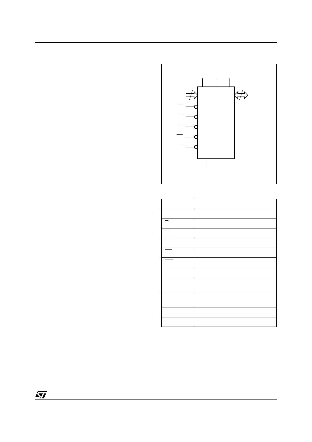
Figure 2. Logic Diagram
V
V
DDQVPP
DD
19
A0-A18
W
E
G
RP
WP
Table 1. Signal Names
A0-A18 Address Inputs
DQ0-DQ15 Data Input/Output
E
G
W
RP
WP
V
DD
M28W800BT
M28W800BB
V
SS
Chip Enable
Output Enable
Write Enable
Reset
Write Protect
Core Power Supply
16
DQ0-DQ15
AI03581
V
DDQ
V
PP
V
SS
NC Not Connected Internally
Power Supply for
Input/Output
Optional Supply Voltage for
Fast Program & Erase
Ground
5/42
M28W800BT, M28W800BB
Figure 3. TSOP Connections
A15
A14
A13
A12
A11
1
48
A16
V
DDQ
V
SS
DQ15
DQ7
A10 DQ14
37
36
DQ6
DQ13
DQ5
DQ12
DQ4
V
DD
DQ11
DQ3
DQ10
DQ2
DQ9
DQ1
DQ8
DQ0
G
V
SS
E
A0
NC
NC
RP
V
PP
WP
NC
A18
A17
A9
A8
W
A7
A6
A5
A4
A3
A2
A1
12
M28W800BT
M28W800BB
13
24 25
AI03582
6/42
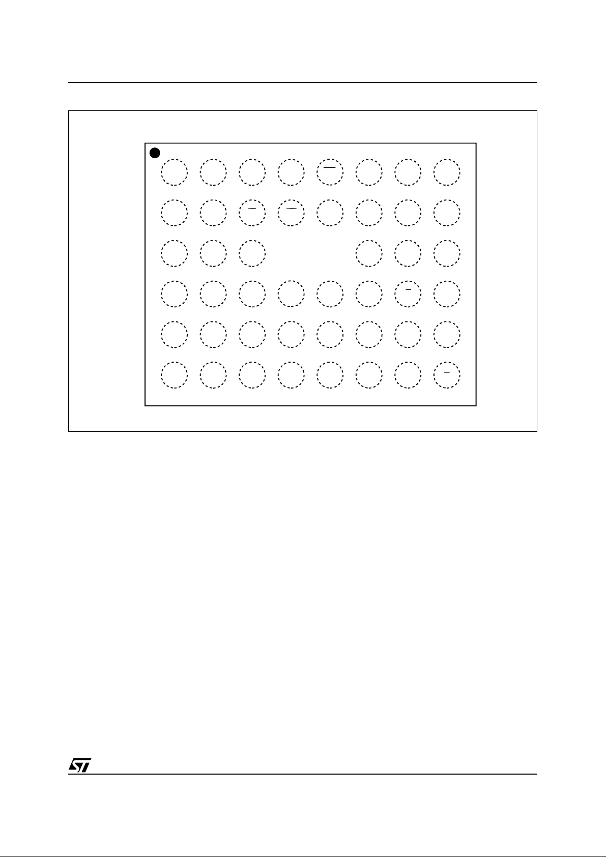
Figure 4. TFBGA Connections (Top view through package)
M28W800BT, M28W800BB
87654321
A
B
C
D
E
F
A13
DDQ
SS
DQ7V
A8A11
DQ13
PP
RP A18
DQ11
DQ12
DQ4
WP
DQ2
DD
NC
A7V
DQ0DQ9DQ3DQ6DQ15V
DQ1DQ10V
A4
A2A5A17WA10A14
A1A3A6A9A12A15
A0EDQ8DQ5DQ14A16
V
SS
G
AI03805
7/42
M28W800BT, M28W800BB
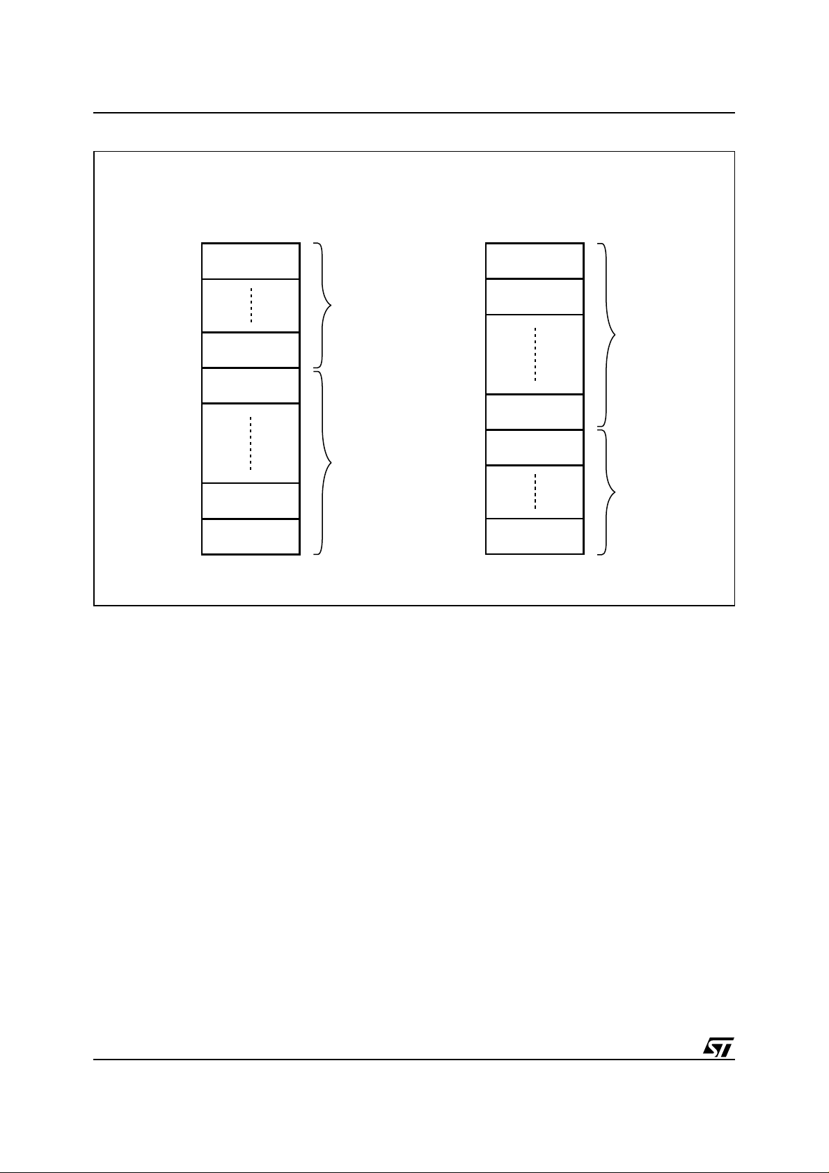
Figure 5. Block Addresses
M28W800BT
Top Boot Block Addresses
7FFFF
7F000
78FFF
78000
77FFF
70000
0FFFF
08000
07FFF
00000
4 KWords
4 KWords
32 KWords
32 KWords
32 KWords
Total of 8
4 KWord Blocks
Total of 15
32 KWord Blocks
M28W800BB
Bottom Boot Block Addresses
7FFFF
78000
77FFF
70000
0FFFF
08000
07FFF
07000
00FFF
00000
32 KWords
32 KWords
32 KWords
4 KWords
4 KWords
Total of 15
32 KWord Blocks
Total of 8
4 KWord Blocks
AI04384
Note: Also see Appendix A, Tables 21 and 22 for a full listing of the Block Addresses.
8/42

SIGNAL DESCRIPTIONS
See Fig ure 2 Logic Diagram and T able 1,Signal
Names, f or a briefoverview of thesignals connected to this device.
Address Inputs (A0-A18). The Address Inputs
select the cells in the memory array to access during Bus Read operations. During Bus Write operations they control the commands sent to the
Command Interface of the internal state machine.
Data Input/Output (DQ0-DQ15). The Data I/O
outputs the data stored at t he s elected address
during aBus Read operation or inputsa command
or data to be programmed during a Write Bus operation.
Chip Enable (E
). The Chip Enable input acti-
vates the memory co ntrol logic, input buffers, decoders andsense amplifiers. When ChipEnable is
and Reset is at VIHthe device is in active
at V
IL
mode. When Chip Enable is at V
the memory is
IH
deselected, the outputs are high impedan ce and
the power consumption is reduced to the stand-by
level.
Output Enable (G
). The Output Ena ble controls
data outputs during the Bus Read operation of the
memory.
WriteEnable(W
). Th e Write Enable controls the
Bus Write operation of the memory’s Command
Interface. Thedata and address inputs are latched
ontherisingedgeofChipEnable,E,orWriteEnable, W
Write Protect (W P
, whichever occurs f irst.
). Write Protect is an input to
protect or unprotect the two lockable parameter
blocks. When Write Protect is at V
, t he lockable
IL
blocks are protected and Program or Erase operations are not possible. When Write Protec t is at
V
, t he lockable blocks are unprotected and can
IH
be programmed or erased (refer to Table 4, Memory Blocks Protection Truth).
Reset (RP
wareresetofthememory.WhenResetisatV
). The Reset input provides a hard-
IL
the memory is in reset mode: the outputs are high
impedance and the current consum pti on is mini-
M28W800BT, M28W800BB
mized. When Reset is at V
mal operation. Exiting reset mode the device
enters read array mode, b ut a negative transition
of Chip Enable or a change of the address is required to ensure v alid data outputs.
Supply Voltage. VDDprovides the power
V
DD
supply to the internal core of the memory device.
It is the main power supply for all operations
(Read, Program and Eras e).
Supply Voltage. V
V
DDQ
power supply to the I/O pins and enables al l Outputs tobe powered independentlyfrom V
canbetiedtoVDDor can use a s eparate supply.
Program Supply Voltage. VPPis both a
V
PP
control input and a power supply pin. The two
functions are selected by the voltage range applied t o the pin. The Supply V olt age V
Program Supply Voltage V
anyorder.
is kept in a low voltage range (0V to 3.6V)
If V
PP
V
is seen as a control input. In this case a volt-
PP
age lowerthan V
PPLK
against program or erase, while V
ables these functions (see Table 11, DC Charac teristics for the relevant values). V
sampled at the beginning of a program or erase; a
change in its value after the operation has started
does not have any effectand program or eraseoperations continue.
is in the range 11.4V to 12.6V it acts as a
If V
PP
power supply pin. In this cond ition V
stable until the Program/Erase al gorithm is completed (see Table 13 and 14).
V
Ground. VSSis the reference for all voltage
SS
measurements.
Note: Each device in a system should have
V
DD,VDDQ
and VPPdecoupled with a 0.1µF capacitor close to the pin. See Figure 7, AC M easurement Load Circu it. Th e PCB trace widths
,
should be sufficient to carry the required V
Program and Erase currents.
, the device is in nor-
IH
DDQ
PP
provides the
canbeappliedin
gives an absolute protection
PP
DD.VDDQ
and the
DD
>V
PP1
is only
PP
must be
PP
en-
PP
9/42
M28W800BT, M28W800BB
BUS OPERATIONS
There are six standard bus operations that control
the device. These are Bus Read, Bus Write, Output Disable, Standby, Aut omatic Standby and Reset. See Table 2, Bus Operations, for a summary.
Typically glitches of less than 5ns on Chip Enable
or Write Enable are ignoredby the memory and do
not affect bus operations.
Read. Read B us opera tions are used to output
the contents of the Memory Array, the Electronic
Signature, the Status Register and the Common
Flash Interface. Both Chip Enable and Output E nablemustbeatV
eration. The Chip Enable input sh ould be used to
enable the device. Output Enable should be used
to gat e data onto the output. The data r ead depends on the previous command written to the
memory (see Command Interface section). See
Figure 8, Read Mode AC Waveforms, and Table
12, Read AC Characteristics, for details of when
the output becomes valid.
Read mode is the default state of the device when
exiting Reset or after power-up.
Write. B us Write ope rations write Commands to
the mem ory or latchInput Data tobe programmed.
A write operation is initiated when Chip Enable
and Write Enable are at V
. Commands, Input Data and Addresses are
V
IH
latched on the rising edge of Write Enable or Chip
Enable, whichever occurs first.
in order t o perform a read op-
IL
with Output Enable at
IL
See Figures 9 and 10, Write AC Waveforms, and
Tables 13 and 14, Write AC Characteristics, for
details of the timing requirements.
Output Disable. The data outputs are high impedance when t he Output Enable is at V
.
IH
Standby. Standby disables most of the internal
circuitryallowing a substantialreduction of the c urrent consumption. The memory is in st and-by
when Chip Enable is at V
andthedeviceisin
IH
read mode. The power consumption is reduced to
the stand-by level and the outputs are set to high
impedance, independently f rom the OutputEnable
or Write Enable inputs. If Chip Enable switches to
V
during a program or erase operation, the de-
IH
vice enters Standby mode when finished.
Automatic Standby. Autom atic Standby pro-
vides a low power consumpt ion state during Read
mode. Following a read operation, the device enters Automatic Standby after 150ns of bus inactivity, even if Chip Enable is low, V
current is reduced to I
. The data Inputs/Out-
DD1
, and the supply
IL
puts will still output data.
Reset. Durin g Res et mode, when Output Enable
is low, V
, the memory is deselected and the out-
IL
puts are high impedance. The memory is in Reset
mode when Reset is at V
. The power cons ump-
IL
tion is reduced to theStan dby level, independently
from the Chip Enable, Output Enable or Write Enable inputs. If Reset is pulled to V
during a Pro-
SS
gram or Eras e, this operation is aborted and the
memory content is no longer valid.
Table 2. Bus Operations
Operation E G W RP WP
Read
Write
Output Disable
Standby
Reset X X X
Note: X = VILor VIH,V
10/42
V
V
V
V
=12V±5%.
PPH
IL
IL
IL
IH
V
IL
V
IH
V
IH
XX
V
IH
V
IL
V
IH
V
IH
V
IH
V
IH
V
IH
V
IL
V
PP
X Don't Care Data Output
V
X
X Don't Care Hi-Z
X Don't Care Hi-Z
X Don't Care Hi-Z
DD
or V
PPH
DQ0-DQ15
Data Input

COMMAND INTERFACE
All Bus Write operations to the memory are interpreted by the Command Interface. Com mands
consist of one or more sequential Bus Write operations. An internal Program/Erase Controller handles all t imings and verifies the correct execution
of the Program and Erase c ommands. The Program/Erase Cont roll er provides a Status Register
whose output may be read at any time, to monitor
the progress of an operation, or the Program/
Erase states. See Appendix D, Table 29, Write
State Machine Current/Next, for a summa ry o f the
Command Interface.
The Command Interface is res et to Read mode
when power is first applied, when exiting from Reset or whenever V
is lower than V
DD
LKO
.Command sequences must be followed exactly. Any
invalid c ombination ofcommands willreset the device to Read mode. Refer to Table 3, Commands,
in conjunction with the text descriptions below.
Read Memory Array command
TheReadcommandreturnsthememorytoits
Read mode. One Bus Write cycle is required to issue the Read Memory Array command and return
the memory to Read mode. Subsequent read operations will read the addressed location and output the data. When a device Reset oc c urs, the
memory defaults to Read mode.
Read Status Register Co m m and
The Status Register indi cates when a program or
erase operation is complete and the success or
failure of the operation itself. Issue a Read Status
Register comma nd to rea d the Stat us Register’s
contents. Subsequent Bus Read operations read
the S tatus Register, at any addres s, until another
command is issued. See Table 7, Status Register
Bits, for details on the definitions of the bits.
The Read Status Regi ster command may be issued at any time, ev en during a Program /Erase
operation. Any Read atte mpt during a Program/
Erase op eration will automatically output the content of the Stat us Register.
Read Electronic Signature Command
The Read Electronic Signature command reads
the Manufacturer and Device Codes.
The Read Electronic Signat ure command consists
of one write cycle, a subsequent read will output
the Manufacturer or the Device Code dependi ng
on the levelsof A0. The Manufacturer Code is output when th e address line A0 is at V
Code is output when A 0 is at V
A7 must be kept to V
, other addresses are ig-
IL
, the Device
IL
. Addres s es A1-
IH
nored. The cod es are output on DQ0-DQ7 with
DQ8-DQ15 at 00h. (see Table 4)
M28W800BT, M28W800BB
Read CFI Query Command
The Read Query Comm and is used to read data
fromtheCommonFlashInterface(CFI)Memory
Area, allowing programm ing equipment or ap plications to automatically match their interface to
the characteristics of the device.
One Bus Write cycle is required to issue the Read
Query Command. Once the c ommand is issued
subsequent Bus Read operations read from the
Common Flash Interface Memory Area. See Appendix B, Common Flash Interface, Tables 23, 24,
25, 26, 27 and 28 for details on the information
contained in the Common Flash Interface memory
area.
Block Erase Command
TheBlockErasecommandcanbeusedtoerase
a block. It setsall the bits within the selected block
to ’1’. All previous data in the block is lost. If the
block is protected then the Erase operation w ill
abort, the data inthe block willnot be changed and
the Status Register will output the error.
Two Bus Write cycles are required to issue the
command.
■ The first bus cycle sets up the Erase command.
■ Th e s ec ond latches the block address in the
internal state machine and starts the P ro gram/
Erase Controller.
If the second bus cycle is not Write Erase Confirm
(D0h), Status Register bits b4 and b5 are set and
the command aborts.
Erase aborts if Reset turns to V
cannot beguaranteed when theErase operation is
aborted, the block must be erased again.
During Erase operations the memory will only accept the Read S tatus Register command and the
Program/Erase Suspend command, allother commands will be ignored. Typical Erase times are
given in Table 6, Program, E ras e Times and Program/Erase Endurance Cycles.
See Appendix C, Figure 19, Erase Flowchart and
Pseudo Code, for the flowchartfor using theErase
command.
Program Command
The memory array can be programmed word-byword. Two bus write cycles are required to issue
the Program command.
■ Th e first bus cycle s ets up the Program
command.
■ Th e secondlatches theAddress andthe Datato
be written and star ts the Program/Erase
Controller.
During Program operations the memory will only
accept the Read Status Register command and
the Program/Erase Suspe nd c ommand. All other
. As dat a integ rity
IL
11/42

M28W800BT, M28W800BB
commands will be ignored. Typical Program times
are given in Table 6, Progra m, E ras e Times and
Program/Erase Endurance Cy c les.
Programming aborts if Reset goes to V
. As data
IL
integrity cannot be guaranteed when the program
operation is aborted, the block containing the
memory location must be erased and reprogrammed.
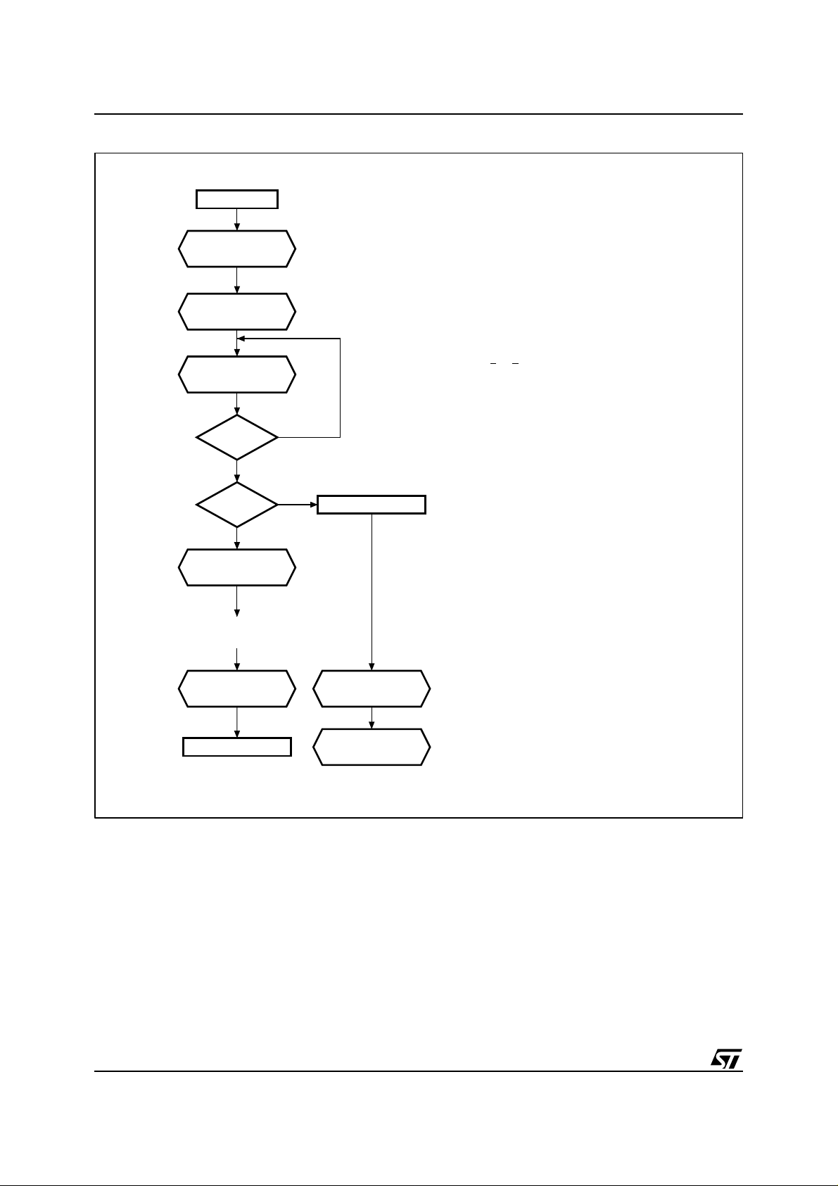
See Appendix C, Figure 16 , Program Flowchart
and Pseudo Code, for the flowchart for using the
Program comman d.
Double Word Program Command
Thisfeat ure isoffered toimprove the programming
throughput, writing a page of two adjacent words
in parallel.The two words must differ only for the
address A0. Programming should not be attempted when V
PP
executed if V
isnot atV
is below V
PP
. The c ommand can be
PPH
but the result is not
PPH
guaranteed.
Three bus write cycles are neces sary to issue the
Double Word Program c ommand.
■ Th e f irst bus cycle sets up the Double Word
Program comm and.
■ The second bus cycle latches the Address and
theDataofthefirstwordtobewritten.
■ The third bus cyclelatches the Address and the
Data of the second word to bewritten and st arts
the Program/Erase Controlle r.
Read operations out put the Status Register content after the programming has started. Programming aborts if Reset goes to V
. As data integrity
IL
cannot be guaranteed when the program operation is aborted, the block containing the memory
location must be erased and reprogrammed.
See Appendix C, Figure 17, Double Word Program Flowchart and Pseudo Code, for the flowchart for using the Double Word Program
command.
Clear Status Register Command
The Clear Status Register command can be used
to reset bits 1, 3, 4 and 5 i n the Status R egister to
‘0’. One bus write cycle is required to issue the
Clear Status Register command.
The bits in the Status Register do not automatically return t o ‘0’ when a new Program or Erase command is issued. Th e error bits in the Status
Register should be cleared before attempting a
new Program or Erase command.
Program/Erase Suspend Command
The Program/Erase Suspend command is used to
pause a Pr ogram or Erase operation. One bus
write cycle is required to issue the Program/Erase
command and pause the Program/Erase cont roller.
During Program/Erase Suspend theCommand Interface will accept the Program/Erase Resume,
Read A rray , Read StatusRegister, Read E lectronic Signature and Read CFI Query commands. Additionally, if the suspend operation was Erase then
the Program command will also be accepted. Only
the blocks not being erased may be read or programmed correctly.
During a Program/Erase Su sp end, the device can
be placed in a pseudo-standby mode by taking
Chip Enable to V
Reset turns to V
. P rogram/Erase is abort ed if
IH
.
IL
See Appendix C, Figure 18, Program Suspend &
Resume Flowchart and Pseudo Code, and Figure
20, Erase Suspend & Res ume Flowchart and
Pseudo Codefor flowchartsfor usingthe Program/
Erase Suspend c ommand.
Program/Erase Resume Command
The Program/Erase Resume command can be
used to restart the Program/Eras e Controller after
a Program/Erase Suspend operation has paused
it. One Bus W rite cycle is required to issue the
command. Once the command is issued subsequent Bus Read operations read the Status Register.
See A ppendix C, Figure 18, Program or Double
Word Program Suspend & Resume Flowchart and
Pseudo Code, and Figure 20, Erase Suspend &
Resume Flowchart and Pseudo Code for flowcharts for using the Program/Erase Resume command.
Block Protection
Two parameter/lockable blocks (blocks #0 and #1)
can be protected against Program or E ras e operations. Unprotected blocks can be program med or
erased.
To protect t he two lockable blocks set Write Protect to V
. WhenVPPis below V
IL
allblocks are
PPLK
protected. Any attempt to Program or Erase protected blocks will abort, the data in the block will
not be changed and the Status Regis ter outputs
the error.
Table 5, Memory Blocks Protection Truth Table,
defines the protection methods.
12/42
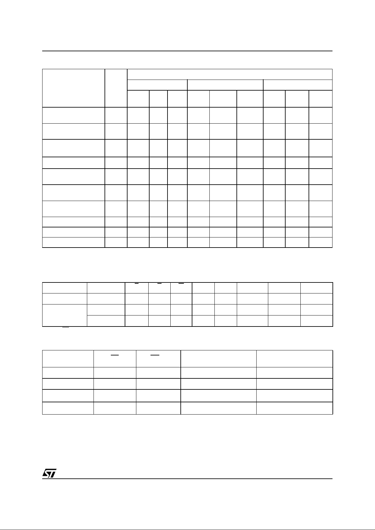
Table 3. Commands
M28W800BT, M28W800BB
Bus Write Operations
(3)
No. of
Cycles
3 Write X 30h Write Addr 1
Commands
Read Memory Array 1+ Write X FFh
Read Status Register 1+ Write X 70h Read X
Read Electronic Signature 1+ Write X 90h
Read CFI Query 1+ Write X 98h
Erase 2 Write X 20h Write
Program 2 Write X
Double Word Program
Clear StatusRegister 1 Write X 50h
Program/Erase Suspend 1 Write X B 0h
Program/Erase Resume 1 Write X D0h
Note: 1. X = Don't Care.
2. A0=V
3. Addr 1 and Addr 2 must be consecutive Addresses differing only for A0.
outputs Manufacturercode,A0=VIHoutputs Device code. Address A7-A1 must be VIL.
IL
1st Cycle 2nd Cycle 3nd Cycle
Bus
Op.
Addr Data
40h or
10h
Bus
Op.
Read
Read
Read
Write Addr
Addr Data
Signature
Addr
CFI Addr Query
Block
Read
Addr
Addr
(2)
Data
Status
Register
Signature
D0h
Data
Input
Data
Input
Bus
Op.
Write Addr 2
Addr Data
Data
Input
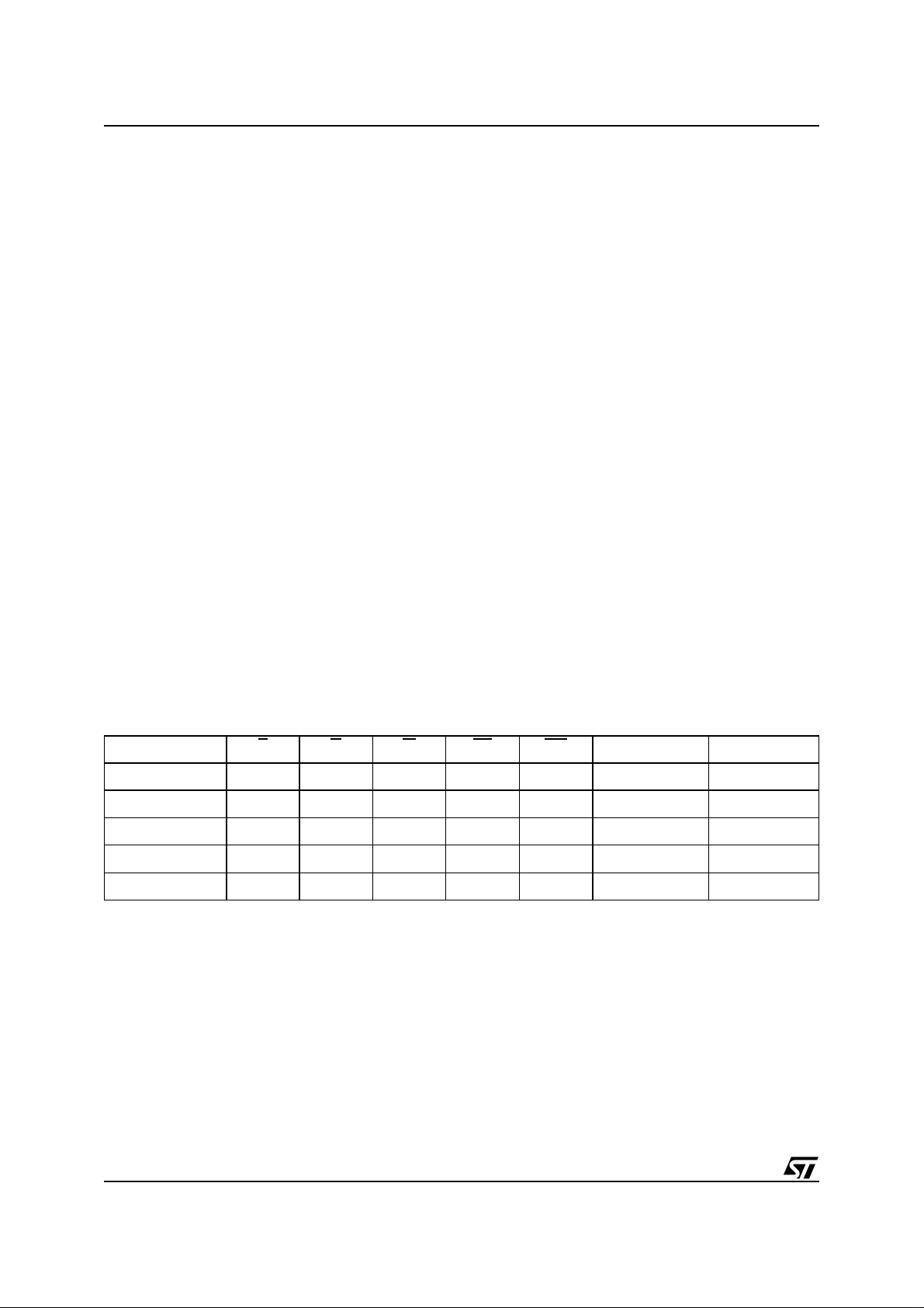
Table 4. Read Electronic Signature
Code Device E G W A0 A1-A7 A8-A18 DQ0-DQ7 DQ8-DQ15
Manufact. Code
Device Code
Note: RP =VIH.
M28W800BT
M28W800BB
V
V
V
V
IL
V
IL
V
IL
V
IL
V
IL
V
IL
V
IH
V
IH
V
IH
V
IL
IH
IH
Don't Care 20h 00h
IL
V
Don't Care 92h 88h
IL
V
Don't Care 93h 88h
IL
Table 5. Memo ry Blocks Protection T ruth Table
(1)
V
PP
X
V
IL
or V
V
DD
or V
V
DD
Note: 1. X = Don't Care
2. V
(2)
PPH
(2)
PPH
must also be greater than the Program Voltage Lock Out V
PP
RP WP
V
IL
V
IH
V
IH
V
IH
(1)
X Protected Protected
X Protected Protected
V
IL
V
IH
Lockable Blocks
(blocks #0 and #1)
Other Blocks
Protected Unprotected
Unprotected Unprotected
.
PPLK
13/42

M28W800BT, M28W800BB
Table 6. Pro gram, Erase Times and Program/Erase Endurance Cycles
Parameter
Test Conditions
M28W800B
Min
Typ
Max
Unit
Word Program
Double Word Program
Main Block Program
V
PP=VDD
VPP=12V±5%
=12V±5%
V
PP
V
PP=VDD
VPP=12V±5%
10 200 µs
10 200 µs
0.16 5 s
0.32 5 s
0.02 4 s
Parameter Block Program
Main Block Erase
V
PP=VDD
=12V±5%
V
PP
V
PP=VDD
VPP=12V±5%
0.04 4 s
110 s
110 s
0.8 10 s
Parameter Block Erase
V
PP=VDD
0.8 10 s
Program/Erase Cycles (per Block) 100,000 cycles
14/42

STATUS REGISTER
The Stat us Register provides information on t he
current or previous Program or Erase operation.
The various bits convey information and errors on
the operation. To read the Status register the
Read S t atu s Register commandcan be issued,refer tothe Read Status RegisterCommand section.
To output the contents, t he Status Register is
latched on the falling edge of the Chip Enable or
Output Enable sign als, and can be read unt il Chip
Enable or Output Enable returns to V
. Eit her
IH
Chip Enable or Output Enable must be toggled to
update the latched data.
Bus R ead operations from any address always
read the Status Register during Program and
Erase operations.
The bits in the Status Register are summarized in
Table 7, Status Register Bits. R efer to Table 7 in
conjunction with the following text descriptions.
Program/Erase Controller Status (Bit 7). The Program/Erase Controller Status bit indi cates whether
the Program/Erase Controller is active or inactive.
When the Program/Erase Controller Status bit is
Low (set to ‘0’), the Program/Erase Controller is
active; when the bit i s High (set to ‘1’), the Program/Erase Controller is inactive, and the device
is ready to process a new command.
The Program/Erase Controller Status is Low immediately after a Program/Erase Suspend command is issued until the Program/Erase Cont roller
pauses. After the Program/Erase Controller pauses the bit is High .
During Program, Erase, operations the Program/
EraseControllerStatusbitcanbepolledtofindthe
end of the operation. Other bit s in the Status Register should not be tested until the Program/Erase
Controller completes the operation and the bit is
High.
After the Program/Erase Controller completes its
operation the Erase Status, Program Status, V
PP
Status and Block Protection Status bits should be
tested for errors.
Erase Suspend Status (Bit 6). T he Erase Suspend Status bit (set to ‘1’) indi ca tes that an Erase
operation has been suspended or is going t o be
suspended.
The Erase Suspend Status should only be considered valid when the Program/Erase ControllerStatus bitis High (Program/Erase Controller inactive).
Bit 7 is set within 30µs of the Program/Erase Sus pend command being issued therefore the memory may still complete the operation rather than
entering the Suspend mode.
When a Program/Erase Resume command is issued the Erase Suspend Status bit re turns Low.
M28W800BT, M28W800BB
Erase Status (Bit 5). The EraseStatus bit ca n be
used to identify if the memory has failed to verify
that the block has erased correctly. When the
Erase Status bit i s High (set to ‘1’), the Program/
Erase Controller has applied the maximum number of pulses to the block and still failed to verify
thatthe block haserased correctly.The Erase Status bit s hould be read once the Program/Erase
Controller Status bit is High (Program/Erase Controller inactive).
Once setHigh, the Erase Status bitcan only be reset Low by a Clear Status Re giste r command or a
hardware reset. If set High it should be reset before a new Program or Eras e command is issued,
otherwise the new command will appear to fail.
Program Status (Bit 4). The Program St atu s bit
is used to identify a Program failure. When the
Program Status bi t is High (set to ‘1’), the Program/Erase Controller has applied the maximum
number of pulses to the byte and still failed to verify that it has programmed correctly. The Program
Status bit should be read once the Program/Erase
Controller Status bit is High (Program/Erase Controller inactive).
Once set High, the Program Status bit can only be
reset Low by a Clear Status Register comm and or
a hardware reset. If set High it should be reset before a new command is issued, otherwise the new
command will appear to fail.
Status (Bit 3). The VPPStatus bit can be
V
PP
used to identify an invalid voltage on the V
during Program and Eras e operations. The V
pin is only sampled at the beginning of a Program
or Erase operation. Indeterminate results can occur if V
When theV
age on theV
when theV
becomes invalid during an operat ion.
PP
Status bitis Low (set to ‘0’),the volt-
PP
pin wassampled at avali d voltage;
PP
Status bit is High (set to‘1’), the V
PP
pin has a voltage th at is below the VPPLockout
Voltage, V
, the memory is protected and Pro-
PPLK
gram and Erase operations cannot be performed.
Onceset High, the V
Status bitcan onlybe reset
PP
Low by a Clear Status Register command or a
hardware reset. If set High it should be reset before a new Program or Eras e command is issued,
otherwise the new command will appear to fail.
Program Suspend Status (Bit 2). The Program
Suspend Status bit (set to ‘1’) indicates that a Program operation has been suspended or is going to
be suspended.
The Program Suspend Status should only be considered valid when the Program/E rase Controller
Status bit is High (Program/Erase Controller inactive). Bit 2 is set within 5µs of the Program/Erase
Suspend command being issued therefore the
PP
pin
PP
PP
15/42

M28W800BT, M28W800BB
memory may still complete the operation rather
than entering the Suspend mode.
When a Program/Erase Resume command is issued t he Program Suspend S tatus bitreturns Low.
Block Protection Status (Bit 1). The Block ProtectionStatusbitcanbeusedtoidentifyifaProgram or Erase operation has tried to modify the
contents of a protected block.
When the B lock Protection Status bit is High (set
Once set High, the Block Protection Status bi t can
only be resetL ow by a Clear Status Register command or a hardware reset. If set High it should be
reset before a new command is issued, otherwise
the new command will appear to fail.
Reserved (Bit 0). Bit 0 of the Status Register is
reserved. Its value must be masked.
Note: Refer to Appendix C, F lowch arts and
Pseudo Codes, for u sing the Status Register.
to ‘1’), a Program or Erase operation has b een attempted on a protect ed block.
Table 7. Status Register Bi ts
Bit Name Logic Level Definition
7 P/E.C. Status
6 Erase Suspend Status
5 Erase Status
4 Program Status
V
3
2 Program Suspend Status
PP
Status
'1' Ready
'0' Busy
'1' Suspended
'0' Inprogress or Completed
'1' Erase Error
'0' Erase Success
'1' Program Error
'0' Program Success
V
'1'
'0'
'1' Suspended
'0' InProgress or Completed
Invalid, Abort
PP
V
OK
PP
1 Block Protection Status
0 Reserved
Note: Logic level '1' is High, '0' is Low.
16/42
'1' Program/Erase on protected Block, Abort
'0' Nooperation to protected blocks

MAXIMUM RATING
Stressingthedeviceabovetheratinglistedinthe
Absolute Maximum Ratings table may c ause permanent damage t o the device. Expos ure to Absolute Maximum Rating conditions for extended
periods may affect device reliability. These are
stress ratings only and operation of the device at
Table 8. Absolute Maximum Ratings
Symbol Parameter
T
A
T
BIAS
T
STG
V
IO
V
DD,VDDQ
V
PP
Note: 1. Depends on range.
Ambient Operating Temperature
Temperature Under Bias –40 125 °C
Storage Temperature –55 155 °C
Input or Output Voltage –0.6
Supply Voltage –0.6 4.1 V
Program Voltage –0.6 13 V
(1)
M28W800BT, M28W800BB
these or any other conditions a bove those indicated in the Operating sections of this specification is
not implied. Refer also to the STMicroele ctronics
SURE Program and other relevant quality doc uments.
Value
Min Max
–40 85 °C
V
+0.6
DDQ
Unit
V
17/42

M28W800BT, M28W800BB
DC AND AC PARAMETERS
This s ec t ion summ arizes the operating and measurement condit ions, and the D C and AC characteristics of the device. The parameters in the DC
and AC characteristics Tables that follow, are derived from tests perform ed under the Measure-
Table 9. Operating and AC Measuremen t Conditions
ment Conditions summarized in Table 9,
Operating and AC Meas urement Conditions. Designers should check that the operating conditions
in their circuit match the measureme nt conditions
when relying on the quoted parameters.
M28W800BT, M28W800BB
Parameter
70 85 90 100
Min Max Min Max Min Max Min Max
Supply Voltage
V
DD
Supply Voltage (V
V
DDQ
DDQ
≤ V
DD
2.7 3.6 2.7 3.6 2.7 3.6 2.7 3.6 V
2.7 3.6 2.7 3.6 2.7 3.6 1.65 3.6 V
)
Ambient Operating Temperature – 40 85 –40 85 – 40 85 – 40 85 °C
Load Capacitance (C
)
L
50 50 50 50 pF
Input Rise and Fall Times 5 5 5 5 ns
Input Pulse Voltages
Input and Output Timing Ref.
Voltages
0toV
V
DDQ
DDQ
/2 V
0toV
DDQ
DDQ
/2 V
0toV
DDQ
DDQ
/2 V
0toV
DDQ
DDQ
/2
Figure 6. AC Measurement I/O Waveform Figure 7. AC Measurement Load Circuit
V
DDQ
V
DDQ
V
/2
DDQ
0V
AI00610
V
DDQ
V
DD
25kΩ
Units
V
V
DEVICE
UNDER
TEST
0.1µF
0.1µF
CL includes JIG capacitance
CL
Table 10. Device Capacitance
Symbol Parameter Test Condition Min Max Unit
V
V
OUT
IN
=0V
=0V
6pF
12 pF
C
IN
C
OUT
Note: Sampled only, not 100% tested.
Input Capacitance
Output Capacitance
18/42
25kΩ
AI00609C
M28W800BT, M28W800BB
Table 11. DC Ch aracteristics
Symbol Parameter Test Condition Min Typ Max Unit
I
LI
I
LO
I
DD
I
DD1
I
DD2
I
DD3
I
DD4
I
DD5
I
PP
I
PP1
I
PP2
I
PP3
I
PP4
V
IL
V
IH
V
OL
V
OH
V
PP1
V
PPH
V
PPLK
V
LKO
Input Leakage Current
Output Leakage Current
Supply Current (Read)
Supply Current (Stand-by or
Automatic Stand-by)
Supply Current
(Reset)
Supply Current (Program)
Supply Current (Erase)
Supply Current
(Program/Erase Suspend)
Program Current
(Read or Stand-by)
Program Current
(Read or Stand-by)
Program Current (Reset)
Program Current (Program)
Program Current (Erase)
Input Low Voltage
Input High Voltage
Output Low Voltage
Output High Voltage
Program Voltage (Program or
Erase operations)
Program Voltage
(Program or Erase
operations)
Program Voltage
(Program and Erase lock-out)
VDDSupply Voltage (Program
and Erase lock-out)
0V≤ V
0V
E
=VSS,G=VIH,f=5MHz
E
RP
RP
Program in progress
V
Program in progress
Erase in progress
V
Erase in progress
E
Erase suspended
RP
Program in progress
V
Program in progress
Erase in progress
V
Erase in progress
I
= 100µA, VDD=VDDmin,
OL
V
DDQ=VDDQ
I
= –100µA, VDD=VDDmin,
OH
V
DDQ=VDDQ
≤ V
IN
DDQ
≤ V
OUT≤VDDQ
=V
=V
DDQ
DDQ
±0.2V,
± 0.2V
=VSS± 0.2V
=12V±5%
PP
V
PP=VDD
=12V±5%
PP
V
PP=VDD
=V
DDQ
V
PP>VDD
≤ V
V
PP
±0.2V,
DD
=VSS± 0.2V
=12V±5%
PP
V
PP=VDD
=12V±5%
PP
V
PP=VDD
≥ 2.7V
V
DDQ
≥ 2.7V 0.7 V
V
DDQ
min
min
±1 µA
±10 µA
10 20 mA
15 50 µA
15 50 µA
10 20 mA
10 20 mA
520mA
520mA
50 µA
400 µA
5µA
5µA
10 mA
5µA
10 mA
5µA
–0.5 0.4 V
–0.5 0.8 V
V
–0.4 V
DDQ
DDQ
V
DDQ
DDQ
+0.4
+0.4
0.1 V
V
–0.1
DDQ
1.65 3.6 V
11.4 12.6 V
1V
2V
V
V
V
19/42

M28W800BT, M28W800BB
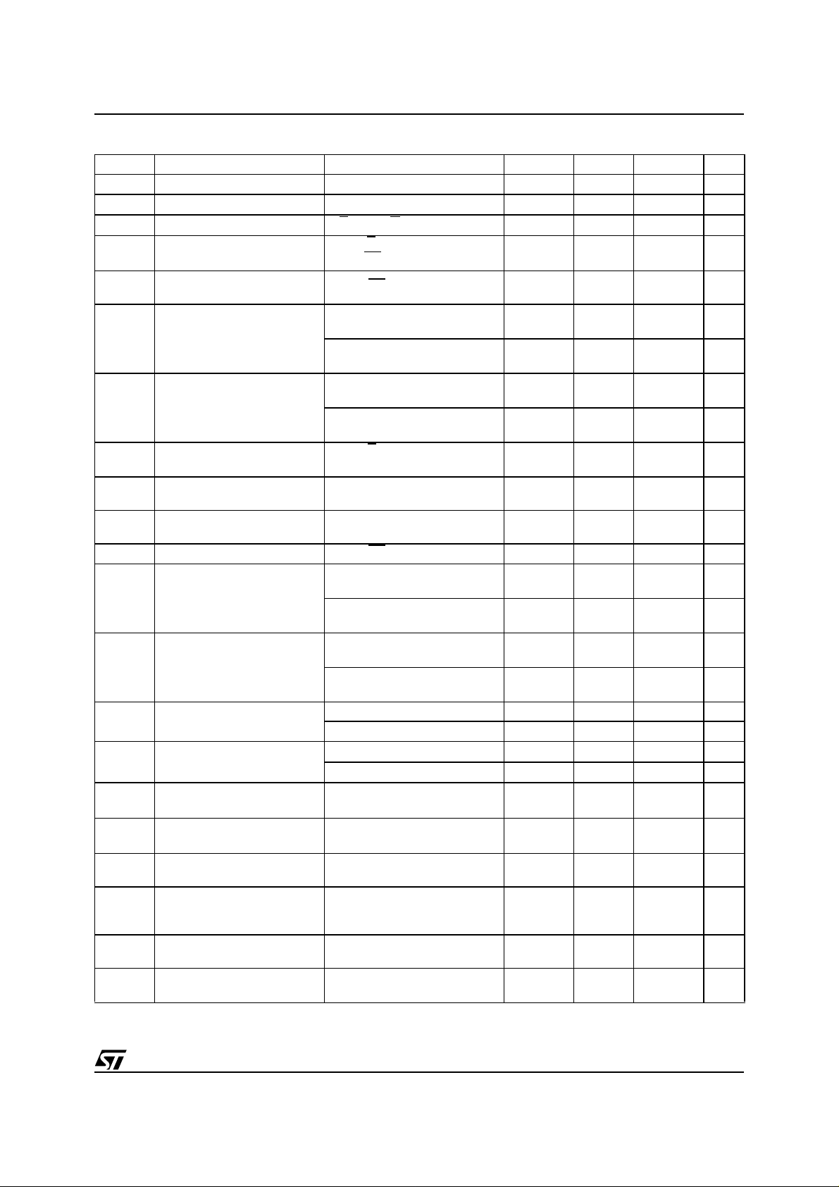
Figure 8. Read AC Waveforms
tAVAV
A0-A18
tAVQV
E
tELQX
G
tGLQX
DQ0-DQ15
ADDR. VALID
CHIP ENABLE
Table 12. Read AC Characteristics
Symbol Alt Parameter
t
AVAV
t
AVQV
t
AXQX
t
EHQX
t
EHQZ
t
ELQV
t
ELQX
t
GHQX
t
GHQZ
t
GLQV
t
GLQX
Note: 1. Sampled only, not 100% tested.
2. G
t
Address Valid to Next Address Valid Min 70 85 90 100 ns
RC
t
Address Valid to Output Valid Max 70 85 90 100 ns
ACC
(1)
t
Address Transition to Output Transition Min 0 0 0 0 ns
OH
(1)
t
Chip Enable High to Output Transition Min 0 0 0 0 ns
OH
(1)
t
Chip Enable High to Output Hi-Z Max 20 20 25 30 ns
HZ
(2)
t
Chip Enable Low to Output Valid Max 70 85 90 100 ns
CE
(1)
t
Chip Enable Low to Output Transition Min 0 0 0 0 ns
LZ
(1)
t
Output Enable High to Output Transition Min 0 0 0 0 ns
OH
(1)
t
Output Enable High to Output Hi-Z Max 20 20 25 30 ns
DF
(2)
t
Output Enable Low to Output Valid Max 20 20 30 35 ns
OE
(1)
t
Output Enable Low to Output Transition Min 0 0 0 0 ns
OLZ
maybe delayed by up to t
ELQV-tGLQV
after the falling edge of E without increasing t
tELQV
tGLQV
OUTPUTS
ENABLED
VALID
tEHQX
tEHQZ
tGHQX
tGHQZ
VALID
DATA VALID STANDBY
M28W800B
70 85 90 100
.
ELQV
tAXQX
AI03578b
Unit
20/42

Figure 9. Write AC Waveforms, Write Enable Controlled
M28W800BT, M28W800BB
AI03579b
tWHAX
PROGRAM OR ERASE
tAVAV
VALIDA0-A18
tAVWH
tWHGL
tELQV
tWHEL
tQVWPL
STATUS REGISTER
tQVVPL
READ
1st POLLING
STATUS REGISTER
OR DATA INPUT
E
tELWL tWHEH
WP
tVPHWH
PP
V
SET-UP COMMAND CONFIRM COMMAND
tWPHWH
tWHWL
G
W
tWHDX
tWLWH
tDVWH
DQ0-DQ15 COMMAND CMD or DATA
21/42

M28W800BT, M28W800BB
Table 13. Write A C Characteristics, Write Enable Controlled
Symbol Alt Parameter
t
AVAV
t
AVWH
t
DVWH
t
ELWL
t
ELQV
(1,2)
t
QVVPL
t
QVWPL
t
VPHWH
t
WHAX
t
WHDX
t
WHEH
t
WHEL
t
WHGL
t
WHWL
t
WLWH
t
WPHWH
Note: 1. Sampled only, not 100% tested.
2. Applicable if V
(1)
t
Write Cycle Time Min 70 85 90 100 ns
WC
t
Address Valid to Write Enable High Min 45 45 50 50 ns
AS
t
Data Valid to Write Enable High Min 45 45 50 50 ns
DS
t
Chip Enable Low to Write Enable Low Min 0 0 0 0 ns
CS
Chip Enable Low to Output Valid Min 70 85 90 100 ns
Output Valid to VPPLow
Min 0 0 0 0 ns
Output Valid to Write Protect Low Min 0 0 0 0 ns
t
VPSVPP
t
AH
t
DH
t
CH
High to Write Enable High
Min 200 200 200 200 ns
Write Enable High to Address Transition Min 0 0 0 0 ns
Write Enable High to Data Transition Min 0 0 0 0 ns
Write Enable High to Chip Enable High Min 0 0 0 0 ns
Write Enable High to Chip Enable Low Min 25 25 30 30 ns
Write Enable High to Output Enable Low Min 20 20 30 30 ns
t
Write Enable High to Write Enable Low Min 25 25 30 30 ns
WPH
t
Write Enable Low to Write Enable High Min 45 45 50 50 ns
WP
Write Protect High to Write Enable High Min 45 45 50 50 ns
is seen as a logic input (VPP<3.6V).
PP
M28W800B
Unit
70 85 90 100
22/42
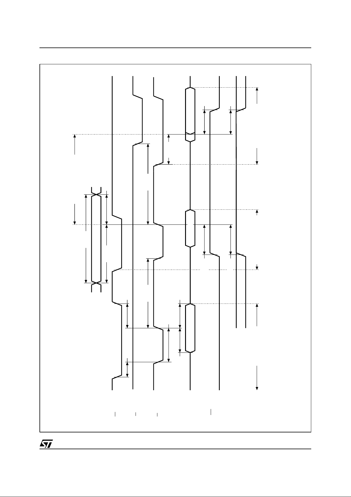
Figure 10. Write AC Waveforms, Chip Enable Controlled
M28W800BT, M28W800BB
AI03580b
tEHAX
PROGRAM OR ERASE
tAVAV
VALIDA0-A18
tAVEH
tEHGL
tELQV
tQVWPL
CMD or DATA STATUS REGISTER
tQVVPL
READ
1st POLLING
STATUS REGISTER
OR DATA INPUT
CONFIRM COMMAND
W
tWLEL tEHWH
WP
tVPHEH
PP
V
POWER-UP AND
SET-UP COMMAND
tWPHEH
tEHEL
G
E
tEHDX
tELEH
tDVEH
DQ0-DQ15 COMMAND
23/42
M28W800BT, M28W800BB
Table 14. Write A C Characteristics, Chip Enable Controlled
Symbol Alt Parameter
t
AVAV
t
AVEH
t
DVEH
t
EHAX
t
EHDX
t
EHEL
t
EHGL
t
EHWH
t
ELEH
t
ELQV
(1,2)
t
QVVPL
t
QVWPL
t
VPHEH
t
WLEL
t
WPHEH
Note: 1. Sampled only, not 100% tested.
2. Applicable if V
(1)
t
Write Cycle Time Min 70 85 90 100 ns
WC
t
Address Valid to Chip Enable High Min 45 45 50 50 ns
AS
t
Data Valid to Chip Enable High Min 45 45 50 50 ns
DS
t
Chip Enable High to Address Transition Min 0 0 0 0 ns
AH
t
Chip Enable High to Data Transition Min 0 0 0 0 ns
DH
t
Chip Enable High to Chip Enable Low Min 25 25 30 30 ns
CPH
Chip Enable High to Output Enable Low Min 25 25 30 30 ns
t
Chip Enable High to Write Enable High Min 0 0 0 0 ns
WH
t
Chip Enable Low to Chip Enable High Min 45 45 50 50 ns
CP
Chip Enable Low to Output Valid Min 70 85 90 100 ns
Output Valid to VPPLow
Min 0 0 0 0 ns
Data Valid to Write Protect Low Min 0 0 0 0 ns
t
VPSVPP
t
CS
High to Chip Enable High
Min 200 200 200 200 ns
Write Enable Low to Chip Enable Low Min 0 0 0 0 ns
Write Protect High to Chip Enable High Min 45 45 50 50 ns
is seen as a logic input (VPP<3.6V).
PP
M28W800B
Unit
70 85 90 100
24/42

Figure 11. Power-Up and Reset AC Wave forms
E, G
W,
RP
tPHWL
tPHEL
tPHGL
M28W800BT, M28W800BB
tPHWL
tPHEL
tPHGL
tVDHPH
VDD, VDDQ
Power-Up Reset
Table 15. Power-Up and Reset AC Characteri stics
Symbol Parameter Test Condition
t
PHWL
t
PHEL
t
PHGL
t
PLPH
t
VDHPH
Note: 1. The device Reset is possible but not guaranteed if t
2. Sampled only, not 100% tested.
3. It is important to assert RP
Reset High to Write Enable Low, Chip
Enable Low, Output Enable Low
(1,2)
Reset Low to Reset High Min 100 100 100 100 ns
(3)
Supply Voltages High to Reset High Min 50 50 50 50 µs
in order to allow proper CPU initialization during power up or reset.
PLPH
During
Program
and Erase
others Min 30 30 30 30 ns
< 100ns.
tPLPH
AI03453b
M28W800B
Unit
70 85 90 100
Min 50 50 50 50 µs
25/42

M28W800BT, M28W800BB
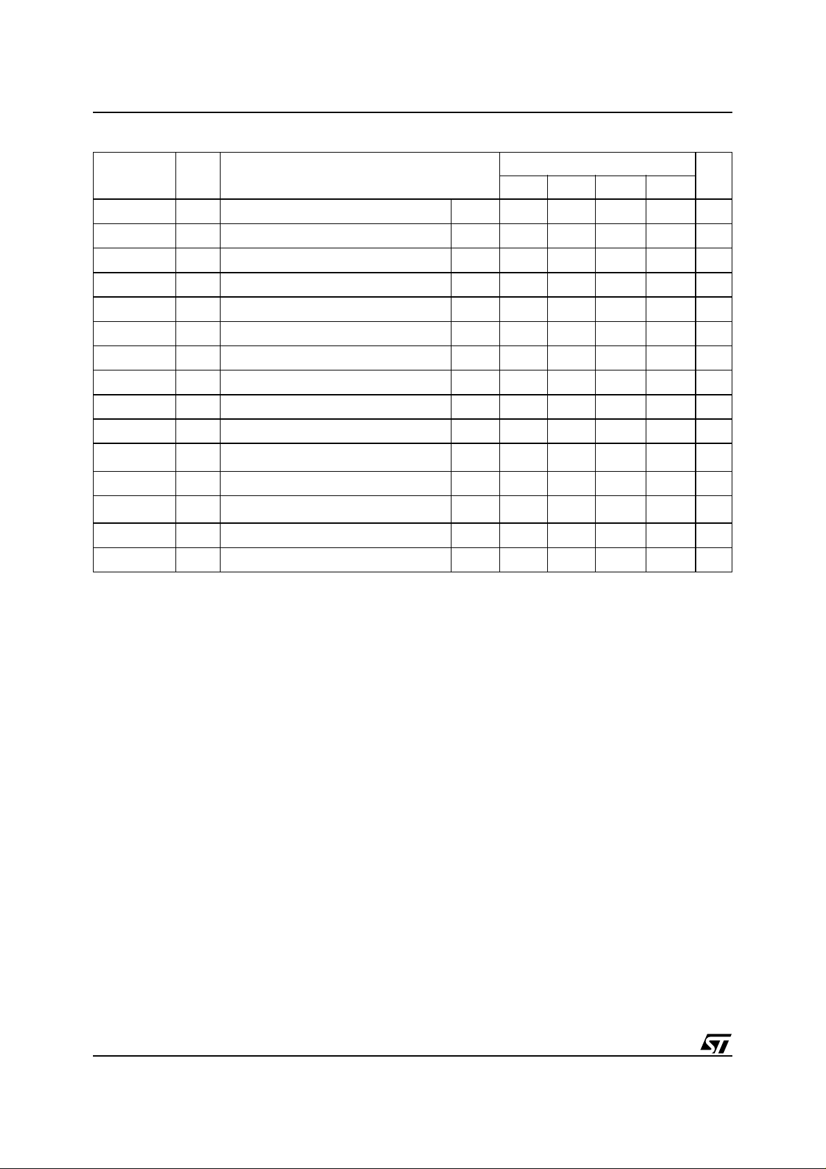
PACKAGE MECHANICAL
Figure 12. TSOP48 - 48 lead Plastic Thin Small Outline, 12 x 20mm, Package Outline
A2
1 N
e
E
B
N/2
D1
D
DIE
A
CP
C
TSOP-a
Note: Drawing is not to scale.
LA1 α
Table 16. TSOP 48 - 48 lead Pla stic Thin Small Outline, 12 x 20mm, Package Mechanical Data
Symbol
A 1.20 0.0472
A1 0.05 0.15 0.0020 0.0059
A2 0.95 1.05 0.0374 0.0413
B 0.17 0.27 0.0067 0.0106
C 0.10 0.21 0.0039 0.0083
D 19.80 20.20 0.7795 0.7953
D1 18.30 18.50 0.7205 0.7283
E 11.90 12.10 0.4685 0.4764
e 0.50 – – 0.0197 – –
L 0.50 0.70 0.0197 0.0279
α 0° 5° 0° 5°
N48 48
CP 0.10 0.0039
Typ Min Max Typ Min Max
mm inches
26/42
M28W800BT, M28W800BB
Figure 13. TFBGA46 6.39x6.37m m - 8x6 ball array, 0.75mm pitch, Bottom View Package Outline
D
FD
FE
SE
E1E
BALL "A1"
D1
SD
e
ddd
A
e
b
A1
A2
BGA-Z13
Drawing is not to scale.
Table 17. TFBGA46 6.39x6.37mm - 8x6 ball array, 0.75m m pitch, Package Mech ani cal Data
Symbol
Typ Min Max Typ Min Max
A 1.200 0.0472
A1 0.200 0.0079
A2 1.000 0.0394
b 0.400 0.350 0.450 0.0157 0.0138 0.0177
D 6.390 6.290 6.490 0.2516 0.2476 0.2555
D1 5.250 – – 0.2067 – –
ddd 0.100 0.0039
E 6.370 6.270 6.470 0.2508 0.2469 0.2547
e 0.750 – – 0.0295 – –
E1 3.750 – – 0.1476 – –
FD 0.570 – – 0.0224 – –
millimeters inches
FE 1.310 – – 0.0516 – –
SD 0.375 – – 0.0148 – –
SE 0.375 – – 0.0148 – –
27/42

M28W800BT, M28W800BB
Figure 14. TFBGA46 Daisy Chain - Package C onnections (Top view through package)
87654321
A
B
C
D
E
F
Figure 15. TFBGA46 Daisy Chain - PCB Connections proposal (Top view through package)
87654321
A
B
C
D
E
F
START
POINT
POINT
AI03860
END
28/42
AI03861

M28W800BT, M28W800BB
PART NUMBERING
Table 18. Ordering Information Scheme
Example: M28W800BT 90 N 6 T
Device Type
M28
Operating Voltage
W=V
Device Function
800B = 8 Mbit (512Kb x16), Boot Block
Array Matrix
T=TopBoot
B = Bottom Boot
Speed
70 = 70 ns
85 = 85 ns
90 = 90 ns
100 = 100 ns
= 2.7V to 3.6V; V
DD
= 1.65V to 3.6V
DDQ
Package
N = TSOP48: 12 x 20 mm
ZB = TFBGA46: 6.39 x 6.37mm, 0.75 mm pitch
Temperature Range
1 = 0 to 70 °C
6 = –40 to 85 °C
Option
T = Tape & Reel Packing
Table 19.Daisy Chain Ordering Scheme
Example: M28W800B -GB T
Device Type
M28W800B
Daisy Chain
-ZB = TFBGA46: 6.39 x 6.37mm, 0.75 mm pitch
Option
T = Tape & Reel Packing
Note:Devices areshipped from thefactory with thememory content bitserased to ’1’.For a listof available
options (Speed, Pack age, etc...) or forfurther information on any aspect of this device, ple as e contact
the ST Sales Office nearest to you.
29/42
M28W800BT, M28W800BB
REVISION HISTORY
Table 20. Docum ent Revision History
Date Version Revision Details
July 1999 -01 First Issue
10-May-2001 -02 Completely rewritten and restructured, 70ns and 85ns speed class added.
29-May-2001 -03 Corrections to CFI data and Block Address Table.
31-May-2001 -04 Package changes - TFBGA45 replaced by TFBGA46.
Document status changed from Preliminary Data to Datasheet
V
Maximum changed to 3.3V
31-Oct-2001 -05
16-May-2002 -06
DDQ
Commands Table, Read CFI Query Address on 1st cycle changed to ‘X’ (Table 3)
description clarified (Table 13)
t
WHEL
V
Maximum changed to 3.6V, TFBGA package dimensions added to description.
DDQ
30/42
APPENDIX A. BLOCK ADDRESS TABLES
M28W800BT, M28W800BB
Table 21. Top Bo ot Block Addresses,
M28W800BT
#
0 4 7F000-7FFFF
1 4 7E000-7EFFF
2 4 7D000-7DFFF
3 4 7C000-7CFFF
4 4 7B000-7BFFF
5 4 7A000-7AFFF
6 4 79000-79FFF
7 4 78000-78FFF
8 32 70000-77FFF
9 32 68000-6FFFF
10 32 60000-67FFF
11 32 58000-5FFFF
12 32 50000-57FFF
13 32 48000-4FFFF
14 32 40000-47FFF
15 32 38000-3FFFF
Size
(KWord)
Address Range
Table 22. Bottom Boot Block Addresses,
M28W800BB
#
22 32 78000-7FFFF
21 32 70000-77FFF
20 32 68000-6FFFF
19 32 60000-67FFF
18 32 58000-5FFFF
17 32 50000-57FFF
16 32 48000-4FFFF
15 32 40000-47FFF
14 32 38000-3FFFF
13 32 30000-37FFF
12 32 28000-2FFFF
11 32 20000-27FFF
10 32 18000-1FFFF
9 32 10000-17FFF
8 32 08000-0FFFF
7 4 07000-07FFF
Size
(KWord)
Address Range
16 32 30000-37FFF
17 32 28000-2FFFF
18 32 20000-27FFF
19 32 18000-1FFFF
20 32 10000-17FFF
21 32 08000-0FFFF
22 32 00000-07FFF
6 4 06000-06FFF
5 4 05000-05FFF
4 4 04000-04FFF
3 4 03000-03FFF
2 4 02000-02FFF
1 4 01000-01FFF
0 4 00000-00FFF
31/42

M28W800BT, M28W800BB
APPENDIX B. COMMON FLASH INTERFACE (CFI)
TheCommonFlashInterfaceisaJEDECapproved, standardized data structure that can be
read from the Flash memory device. It allows a
system software to query the device to determine
various electrical and timing param eters, density
information and functions supported by the memory. The system can i nterface easily with the device, enabling th e software to upgrad e itself when
necessary.
When the CFI Query Command (RCFI) is issued
the device enters CFI Query mode and the data
Table 23. Query Structure Overview
Offset Sub-section Name Description
00h Reserved Reserved for algorithm-specific information
10h CFI Query Identification String Command set ID and algorithm data offset
1Bh System Interface Information Device timing & voltage information
27h Device Geometry Definition Flash device layout
P Primary Algorithm-specific Extended Query table
A Alternate Algorithm-specific Extended Query table
Note: Query data are alwayspresentedon the lowest orderdata outputs.
structure is read from the m emory. Tables 23, 24,
25, 26, 27 and 28 show the addresses us ed to retrieve the data.
The CFI data structu re also contains a security
area where a 64 bit unique security number iswritten (see Table 28, Security Code area). T his area
can be accessed only in Read mode by the final
user. It is im pos sible to change the security number after it has been written by ST. Issue a Read
command to return to Read mode.
Additional information specific to the Primary
Algorithm (optional)
Additional information specific to the Alternate
Algorithm (optional)
Table 24. CFI Query Identification String
Offset Data Description Value
00h 0020h Manufacturer Code ST
01h
02h-0Fh reserved Reserved
10h 0051h Query Unique ASCII String "QRY" “Q”
11h 0052h Query Unique ASCII String "QRY" “R”
12h 0059h Query Unique ASCII String "QRY" “Y”
13h 0003h
14h 0000h
15h
16h 0000h
17h 0000h
18h 0000h
19h
1Ah 0000h
Note: Query data are always presented on the lowest order data outputs (DQ7-DQ0) only. DQ8-DQ15 are ‘0’.
8892h
8893h
offset = P =
0035h
value = A =
0000h
Device Code
Primary Algorithm Command Set and Control Interface ID code 16 bit ID
code defining a specific algorithm
Address for Primary Algorithm extended Query table
Alternate Vendor Command Set and Control Interface ID Code second
vendor - specified algorithm supported (note: 0000h means none exists)
Address for Alternate Algorithm extended Query table
note: 0000h means none exists
Compatible
Top
Bottom
Intel
P=35h
NA
NA
32/42
M28W800BT, M28W800BB
Table 25. CFI Query System Interface Information
Offset Data Description Value
Logic Supply Minimum Program/Erase or Write voltage
V
1Bh 0027h
1Ch 0036h
1Dh 00B4h
1Eh 00C6h
1Fh 0004h
20h 0004h
21h 000Ah
22h 0000h
23h 0005h
24h 0005h
25h 0003h
26h 0000h
DD
bit 7 to 4 BCD value in volts
bit 3 to 0 BCD value in 100 mV
Logic Supply Maximum Program/Erase or Write voltage
V
DD
bit 7 to 4 BCD value in volts
bit 3 to 0 BCD value in 100 mV
[Programming] Supply Minimum Program/Erase voltage
V
PP
bit 7 to 4 HEX value in volts
bit 3 to 0 BCD value in 100 mV
[Programming] Supply Maximum Program/Erase voltage
V
PP
bit 7 to 4 HEX value in volts
bit 3 to 0 BCD value in 100 mV
n
Typical timeout per single word program = 2
Typical timeout for Double Word Program = 2
Typical timeout per individual block erase = 2
Typical timeout for full chip erase = 2
n
Maximum timeout for word program = 2
Maximum timeout for Double Word Program = 2
Maximum timeout per individual block erase = 2
n
Maximum timeout for chip erase = 2
times typical
µs
n
n
ms
n
times typical
µs
ms
n
times typical
n
times typical
2.7V
3.6V
11.4V
12.6V
16µs
16µs
1s
NA
512µs
512µs
8s
NA
33/42

M28W800BT, M28W800BB
Table 26. Device Geometry Definition
Offset Word
Mode
27h 0014h
28h
29h
2Ah
2Bh
2Ch 0002h Number of Erase Block Regions within the device.
2Dh
2Eh
2Fh
30h
31h
32h
M28W800BT
33h
34h
2Dh
2Eh
2Fh
30h
31h
32h
M28W800BB
33h
34h
Data Description Value
n
in number of bytes
0001h
0000h
0002h
0000h
000Eh
0000h
0000h
0001h
0007h
0000h
0020h
0000h
0007h
0000h
0020h
0000h
000Eh
0000h
0000h
0001h
Device Size = 2
Flash Device Interface Code description
Maximum number of bytes in multi-byte program or page = 2
It specifies the number of regions within the device containing contiguous
Erase Blocks of the same size.
Region 1 Information
Number of identical-size erase block = 000Eh+1
Region 1 Information
Block size in Region 1 = 0100h * 256 byte
Region 2 Information
Number of identical-size erase block = 0007h+1
Region 2 Information
Block size in Region 2 = 0020h * 256 byte
Region 1 Information
Number of identical-size erase block = 0007h+1
Region 1 Information
Block size in Region 1 = 0020h * 256 byte
Region 2 Information
Number of identical-size erase block = 000Eh+1
Region 2 Information
Block size in Region 2 = 0100h * 256 byte
1MByte
x16
Async
n
4
2
15
64KByte
8
8KByte
8
8KByte
15
64KByte
34/42

M28W800BT, M28W800BB
Table 27. Primary Algorithm-Specific Extend ed Query Table
Offset
P = 35h
(1)
(P+0)h = 35h 0050h
(P+1)h = 36h 0052h "R"
(P+2)h = 37h 0049h "I"
(P+3)h = 38h 0031h Major version number, ASCII "1"
(P+4)h = 39h 0030h Minor version number, ASCII "0"
Data Description Value
Primary Algorithm extended Query table unique ASCII string “PRI”
"P"
(P+5)h = 3Ah 0006h Extended Query table contents for Primary Algorithm. Address (P+5)h
(P+6)h = 3Bh 0000h
(P+7)h = 3Ch 0000h
(P+8)h = 3Dh 0000h
contains less significant byte.
bit 0 Chip Erase supported (1 = Yes, 0 = No)
bit 1 Erase Suspend supported (1 = Yes, 0 = No)
bit 2 Program Suspend (1 = Yes, 0 = No)
bit 3 Lock/Unlock supported (1 = Yes, 0 = No)
bit 4 Queued Erase supported (1 = Yes, 0 = No)
bit 31 to 5 Reserved; undefined bits are ‘0’
(P+9)h = 3Eh 0001h Supported Functions after Suspend
Read Array, Read Status Register and CFI Query are always supported
during Erase or Program operation
bit 0 Program supported after Erase Suspend (1 = Yes, 0 = No)
bit 7 to 1 Reserved; undefined bits are ‘0’
(P+A)h = 3Fh 0000h Block Lock Status
(P+B)h = 40h 0000h
Defines which bits in the Block Status Register section of the Query are
implemented.
bit 0 Block Lock Status Register Lock/Unlock bit active(1 = Yes, 0 = No)
bit 1 Block Lock Status Register Lock-Down bit active (1 = Yes,0 = No)
bit 15 to 2 Reserved for future use; undefined bits are ‘0’
(P+C)h = 41h 0030h V
Logic Supply Optimum Program/Erase voltage (highest performance)
DD
bit 7 to 4 HEX value in volts
bit 3 to 0 BCD value in 100 mV
(P+D)h = 42h 00C0h V
Supply Optimum Program/Erase voltage
PP
No
Yes
Yes
No
No
Yes
NA
3V
12V
bit 7 to 4 HEX value in volts
bit 3 to 0 BCD value in 100 mV
(P+E)h 0000h Reserved
Note: 1. See Table 24, offset 15h for P pointer definition.
Table 28. Security Code Area
Offset Data Description
81h XXXX
82h XXXX
83h XXXX
84h XXXX
64 bits unique device number.
35/42

M28W800BT, M28W800BB
APPENDIX C. FLOWCHARTS AND P SEUDO CODES
Figure 16. Program Flowchart and Pseudo Code
Start
Write 40h or 10h
Write Address
& Data
Read Status
Register
b7 = 1
YES
b3 = 0
YES
b4 = 0
YES
b1 = 0
YES
End
NO
NO
NO
NO
VPP Invalid
Error (1, 2)
Program
Error (1, 2)
Program to Protected
Block Error (1, 2)
program_command (addressToProgram, dataToProgram) {:
writeToFlash (any_address, 0x40) ;
/*or writeToFlash (any_address, 0x10) ; */
writeToFlash (addressToProgram, dataToProgram) ;
/*Memory enters read status state after
the Program Command*/
do {
status_register=readFlash (any_address) ;
/* E or G must be toggled*/
} while (status_register.b7== 0) ;
if (status_register.b3==1) /*VPP invalid error */
error_handler ( ) ;
if (status_register.b4==1) /*program error */
error_handler ( ) ;
if (status_register.b1==1) /*program to protect block error */
error_handler ( ) ;
}
AI03538b
Note: 1. Status check of b1 (Protected Block), b3 (VPPInvalid) and b4 (Program Error) can be made after each program operation or after
a sequence.
2. If an error is found, the Status Register must be cleared before further Program/Erase Controller operations.
36/42

Figure 17. Double Word Program Flowchart and Pseudo Code
Start
M28W800BT, M28W800BB
Write 30h
Write Address 1
& Data 1 (3)
Write Address 2
& Data 2 (3)
Read Status
Register
b7 = 1
YES
b3 = 0
YES
b4 = 0
NO
NO
NO
VPP Invalid
Error (1, 2)
Program
Error (1, 2)
double_word_program_command (addressToProgram1, dataToProgram1,
addressToProgram2, dataToProgram2)
{
writeToFlash (any_address, 0x30) ;
writeToFlash (addressToProgram1, dataToProgram1) ;
/*see note (3) */
writeToFlash (addressToProgram2, dataToProgram2) ;
/*see note (3) */
/*Memory enters read status state after
the Program command*/
do {
status_register=readFlash (any_address) ;
/* E or G must be toggled*/
} while (status_register.b7== 0) ;
if (status_register.b3==1) /*VPP invalid error */
error_handler ( ) ;
if (status_register.b4==1) /*program error */
error_handler ( ) ;
YES
NO
b1 = 0
YES
End
Note: 1. Status check of b1 (Protected Block), b3 (VPPInvalid) and b4 (Program Error) can be made after each program operation or after
a sequence.
2. If an error is found, the Status Register must be cleared before further Program/Erase operations.
3. Address 1 and Address 2 must be consecutive addresses differing only for bit A0.
Program to Protected
Block Error (1, 2)
if (status_register.b1==1) /*program to protect block error */
error_handler ( ) ;
}
AI03539b
37/42
M28W800BT, M28W800BB
Figure 18. Prog ram Suspend & Resume Flowchart and Pseudo Code
Start
program_suspend_command ( ) {
Write B0h
Write 70h
Read Status
Register
writeToFlash (any_address, 0xB0) ;
writeToFlash (any_address, 0x70) ;
/* read status register to check if
program has already completed */
do {
status_register=readFlash (any_address) ;
/* E or G must be toggled*/
b7 = 1
YES
b2 = 1
YES
Write FFh
Read data from
another address
Write D0h
Program Continues
NO
NO
Program Complete
Write FFh
Read Data
} while (status_register.b7== 0) ;
if (status_register.b2==0) /*program completed */
{ writeToFlash (any_address, 0xFF) ;
read_data ( ) ; /*read data from another block*/
/*The device returns to Read Array
(as if program/erase suspend was not issued).*/
}
else
{ writeToFlash (any_address, 0xFF) ;
read_data ( ); /*read data from another address*/
writeToFlash (any_address, 0xD0) ;
/*write 0xD0 to resume program*/
}
}
AI03540b
38/42

Figure 19. Erase Flowchart and Pseudo Code
Start
Write 20h
Write Block
Address & D0h
M28W800BT, M28W800BB
erase_command ( blockToErase ) {
writeToFlash (any_address, 0x20) ;
writeToFlash (blockToErase, 0xD0) ;
/* only A12-A20 are significannt */
/* Memory enters read status state after
the Erase Command */
Read Status
Register
YES
YES
NO
YES
YES
NO
NO
YES
NO
NO
VPP Invalid
Error (1)
Command
Sequence Error (1)
Erase to Protected
Block Error (1)
b7 = 1
b3 = 0
b4, b5 = 1
b5 = 0 Erase Error (1)
b1 = 0
End
do {
status_register=readFlash (any_address) ;
/* E or G must be toggled*/
} while (status_register.b7== 0) ;
if (status_register.b3==1) /*VPP invalid error */
error_handler ( ) ;
if ( (status_register.b4==1) && (status_register.b5==1) )
/* command sequence error */
error_handler ( ) ;
if ( (status_register.b5==1) )
/* erase error */
error_handler ( ) ;
if (status_register.b1==1) /*program to protect block error */
error_handler ( ) ;
}
AI03541b
Note: If an error is found, the Status Register must be cleared before further Program/Erase operations.
39/42

M28W800BT, M28W800BB
Figure 20. Erase Suspend & Resu m e Flowchart and Pseudo Code
Start
Write B0h
Write 70h
Read Status
Register
b7 = 1
YES
b6 = 1
YES
Write FFh
Read data from
another block
or
Program
Write D0h
Erase Continues
NO
NO
Erase Complete
Write FFh
Read Data
erase_suspend_command ( ) {
writeToFlash (any_address, 0xB0) ;
writeToFlash (any_address, 0x70) ;
/* read status register to check if
erase has already completed */
do {
status_register=readFlash (any_address) ;
/* E or G must be toggled*/
} while (status_register.b7== 0) ;
if (status_register.b6==0) /*erase completed */
{ writeToFlash (any_address, 0xFF) ;
read_data ( ) ;
/*read data from another block*/
/*The device returns to Read Array
(as if program/erase suspend was not issued).*/
}
else
{ writeToFlash (any_address, 0xFF) ;
read_program_data ( );
/*read or program data from another address*/
writeToFlash (any_address, 0xD0) ;
/*write 0xD0 to resume erase*/
}
}
40/42
AI03549b

M28W800BT, M28W800BB
APPENDIX D. COMMAND INTERFACE AND PROGRAM/ERASE CONTROLLER STATE
Table 29. Write State Machine Current/Next
Command Input (and Next State)
Current
StateSRbit 7
Read
Array
Read
Status
Read
Elect.Sg.
Program
Setup
Program
(continue)
Program
Suspend
to Read
Status
Program
Suspend
to Read
Array
Program
Suspend
to Read
Elect.Sg.
Program
(complete)
Erase
Setup
Erase
Cmd.
Error
Erase
(continue)
Erase
Suspend
to Read
Status
Erase
Suspend
to Read
Array
Erase
Suspend
to Read
Elect.Sg.
Erase
(complete)
Note: Elect.Sg . = Electronic Signature.
Data
When
Read
“1” Array
“1” Status
Electronic
“1”
Signature
“1” Status Program (Command input = Data to be Programmed)
“0” Status Program(continue)
“1” Status
“1” Array
Electronic
“1”
Signature
“1” Status
“1” Status Erase Command Error
“0” Status
“1” Status Erase (continue)
“1” Status
“1” Array
Electronic
“1”
Signature
“1” Status
Read
Array
(FFh)
Read
Array
Read
Array
Read
Array
Program
Suspend
to Read
Array
Program
Suspend
to Read
Array
Program
Suspend
to Read
Array
Read
Array
Read
Array
Erase
Suspend
to Read
Array
Erase
Suspend
to Read
Array
Erase
Suspend
to Read
Array
Read
Array
Program
Setup
(10/40h)
Program
Setup
Program
Setup
Program
Setup
Program Suspend to
Program Suspend to
Program Suspend to
Program
Setup
Program
Setup
Program
Setup
Program
Setup
Program
Setup
Program
Setup
Erase
Setup
(20h)
Erase
Setup
Erase
Setup
Erase
Setup
Read Array
Read Array
Read Array
Erase
Setup
Erase
Setup
Erase
Suspend
to Read
Array
Erase
Suspend
to Read
Array
Erase
Suspend
to Read
Array
Erase
Setup
Erase
Confirm
(D0h)
Program
(continue)
Program
(continue)
Program
(continue)
Erase
(continue)
Erase
(continue)
Erase
(continue)
Erase
(continue)
Program/
Erase
Suspend
(B0h)
Read Array
Read Array
Read Array
Program
Suspend
to Read
Status
Program
Suspend
to Read
Array
Program
Suspend
to Read
Array
Program
Suspend
to Read
Array
Read Array
Erase
Command
Error
Read Array
Erase
Suspend
to Read
Status
Erase
Suspend
to Read
Array
Erase
Suspend
to Read
Array
Erase
Suspend
to Read
Array
Read Array
Program/
Erase
Resume
(D0h)
Program
(continue)
Program
(continue)
Program
(continue)
Erase
(continue)
Erase
(continue)
Erase
(continue)
Erase
(continue)
Read
Status
(70h)
Read
Status
Read
Status
Read
Status
Program (continue)
Program
Suspend
to Read
Status
Program
Suspend
to Read
Status
Program
Suspend
to Read
Status
Read
Status
Read
Status
Erase (continue)
Erase
Suspend
to Read
Status
Erase
Suspend
to Read
Status
Erase
Suspend
to Read
Status
Read
Status
Clear
Status
(50h)
Read
Array
Read
Array
Read
Array
Program
Suspend
to Read
Array
Program
Suspend
to Read
Array
Program
Suspend
to Read
Array
Read
Array
Erase Command Error
Read
Array
Erase
Suspend
to Read
Array
Erase
Suspend
to Read
Array
Erase
Suspend
to Read
Array
Read
Array
Read
Elect.Sg.
(90h)
Read
Elect.Sg.
Read
Elect.Sg.
Read
Elect.Sg.
Program
Suspend
to Read
Elect.Sg.
Program
Suspend
to Read
Elect.Sg.
Program
Suspend
to Read
Elect.Sg.
Read
Elect.Sg.
Read
Elect.Sg.
Erase
Suspend
to Read
Elect.Sg.
Erase
Suspend
to Read
Elect.Sg.
Erase
Suspend
to Read
Elect.Sg.
Read
Elect.Sg.
41/42

M28W800BT, M28W800BB
Information furnished is believed to be accurate and reliable. However, STMicroelectronics assumes no responsibility for the consequences
of use of such information nor for any infringement of patents or other rights of third parties which may result from its use.No license is granted
by implication or otherwise under any patent or patent rights of STMicroelectronics. Specifications mentioned in this publication are subject
to change without notice. This publication supersedes and replaces all information previously supplied. STMicroelectronics products are not
authorized for use as critical components in life support devices or systems without express written approval of STMicroelectronics.
The ST logo is registered trademark of STMicroelectronics
All other names are the property of their respective owners.
2002 STMicroelectronics - All Rights Reserved
Australia - Brazil - Canada - China - Finland - France - Germany - Hong Kong - India - Israel - Italy - Japan - Malaysia - Malta -
Morocco - Singapore - Spain - Sweden - Switzerland - United Kingdom - United States
STMicroelectronics GROUP OF COMPANIES
www.st.com
42/42
 Loading...