

FEATURES SUMMARY
■ SUPPLY VOLTAGE
= 2.7V to 3.6V Core Power Supply
–V
DD
–V
–V
■ ACCESS TIME: 70, 85, 90,100ns
■ PROGRAMMING TIME:
= 1.65V to 3.6V for Input/Output
DDQ
= 12V for fast Program (optional)
PP
– 10µ s typical
– Double Word Programming Option
– Quadruple Word Programming Option
■ COMMON FLASH INTERFACE
■ MEMORY BLOCKS
– Parameter Blocks (Top or Bott o m location)
– Main Blocks
■ BLOCK LOCKING
– All blocks locked at Power Up
– Any combination of blocks can be locked
for Block Lock-Down
–WP
■ SECURITY
– 128 bit user Programmable OTP cells
– 64 bit unique device identifier
■ AUTOMATIC STAND-BY MODE
■ PROGRAM and ERASE SUSPEND
■ 100,000 PROGRAM/ERASE CYCLES per
BLOCK
■ ELECTRONIC SIGNATURE
– Manufacturer Code: 20h
– Top Device Code, M28W640ECT: 8848h
– Bottom Device Code, M28W640ECB: 8849h
M28W640ECT
M28W640ECB
64 Mbit (4Mb x16, Boot Block)
3V Supp l y Fl ash Mem ory
PRELIMINARY DATA
Figure 1. Packages
FBGA
TFBGA48 (ZB)
6.39 x 10.5mm
TSOP48 (N)
12 x 20mm
April 2003
This is preliminary information on a new product now in development or undergoing evaluation. Details are subject to change without notice.
1/55

M28W640ECT, M28W640ECB
TABLE OF CONTENTS
SUMMARY DESCRIPTION. . . . . . . . . . . . . . . . . . . . . . . . . . . . . . . . . . . . . . . . . . . . . . . . . . . . . . . . . . . 5
Figure 2. Logic Diagram . . . . . . . . . . . . . . . . . . . . . . . . . . . . . . . . . . . . . . . . . . . . . . . . . . . . . . . . . . 5
Table 1. Signal Names . . . . . . . . . . . . . . . . . . . . . . . . . . . . . . . . . . . . . . . . . . . . . . . . . . . . . . . . . . . 5
Figure 3. TSOP Connections . . . . . . . . . . . . . . . . . . . . . . . . . . . . . . . . . . . . . . . . . . . . . . . . . . . . . . . 6
Figure 4. TFBGA Connections (Top view through package). . . . . . . . . . . . . . . . . . . . . . . . . . . . . . . 7
Figure 5. Block Addresses. . . . . . . . . . . . . . . . . . . . . . . . . . . . . . . . . . . . . . . . . . . . . . . . . . . . . . . . . 8
Figure 6. Protection Register Memory Map. . . . . . . . . . . . . . . . . . . . . . . . . . . . . . . . . . . . . . . . . . . . 8
SIGNAL DESCRIPTIONS . . . . . . . . . . . . . . . . . . . . . . . . . . . . . . . . . . . . . . . . . . . . . . . . . . . . . . . . . . . . 9
Address Inputs (A0-A21). . . . . . . . . . . . . . . . . . . . . . . . . . . . . . . . . . . . . . . . . . . . . . . . . . . . . . . . . . 9
Data Input/Output (DQ0-DQ15). . . . . . . . . . . . . . . . . . . . . . . . . . . . . . . . . . . . . . . . . . . . . . . . . . . . . 9
Chip Enable (E). . . . . . . . . . . . . . . . . . . . . . . . . . . . . . . . . . . . . . . . . . . . . . . . . . . . . . . . . . . . . . . . . 9
Output Enable (G). . . . . . . . . . . . . . . . . . . . . . . . . . . . . . . . . . . . . . . . . . . . . . . . . . . . . . . . . . . . . . . 9
Write Enable (W). . . . . . . . . . . . . . . . . . . . . . . . . . . . . . . . . . . . . . . . . . . . . . . . . . . . . . . . . . . . . . . . 9
Write Protect (WP). . . . . . . . . . . . . . . . . . . . . . . . . . . . . . . . . . . . . . . . . . . . . . . . . . . . . . . . . . . . . . . 9
Reset (RP). . . . . . . . . . . . . . . . . . . . . . . . . . . . . . . . . . . . . . . . . . . . . . . . . . . . . . . . . . . . . . . . . . . . . 9
V
Supply Voltage. . . . . . . . . . . . . . . . . . . . . . . . . . . . . . . . . . . . . . . . . . . . . . . . . . . . . . . . . . . . . . 9
DD
V
Supply Voltage. . . . . . . . . . . . . . . . . . . . . . . . . . . . . . . . . . . . . . . . . . . . . . . . . . . . . . . . . . . . . 9
DDQ
V
Program Supply Voltage . . . . . . . . . . . . . . . . . . . . . . . . . . . . . . . . . . . . . . . . . . . . . . . . . . . . . . 9
PP
V
Ground. . . . . . . . . . . . . . . . . . . . . . . . . . . . . . . . . . . . . . . . . . . . . . . . . . . . . . . . . . . . . . . . . . . . 9
SS
BUS OPERATIONS. . . . . . . . . . . . . . . . . . . . . . . . . . . . . . . . . . . . . . . . . . . . . . . . . . . . . . . . . . . . . . . . 10
Read.. . . . . . . . . . . . . . . . . . . . . . . . . . . . . . . . . . . . . . . . . . . . . . . . . . . . . . . . . . . . . . . . . . . . . . . . 1 0
Write.. . . . . . . . . . . . . . . . . . . . . . . . . . . . . . . . . . . . . . . . . . . . . . . . . . . . . . . . . . . . . . . . . . . . . . . . 10
Output Disable. . . . . . . . . . . . . . . . . . . . . . . . . . . . . . . . . . . . . . . . . . . . . . . . . . . . . . . . . . . . . . . . . 1 0
Standby. . . . . . . . . . . . . . . . . . . . . . . . . . . . . . . . . . . . . . . . . . . . . . . . . . . . . . . . . . . . . . . . . . . . . . 10
Automatic Standby. . . . . . . . . . . . . . . . . . . . . . . . . . . . . . . . . . . . . . . . . . . . . . . . . . . . . . . . . . . . . . 10
Reset. . . . . . . . . . . . . . . . . . . . . . . . . . . . . . . . . . . . . . . . . . . . . . . . . . . . . . . . . . . . . . . . . . . . . . . . 10
Read Electronic Signature Comma nd . . . . . . . . . . . . . . . . . . . . . . . . . . . . . . . . . . . . . . . . . . . . . . . 11
Table 2. Bus Operations . . . . . . . . . . . . . . . . . . . . . . . . . . . . . . . . . . . . . . . . . . . . . . . . . . . . . . . . . 10
COMMAND INTERFACE . . . . . . . . . . . . . . . . . . . . . . . . . . . . . . . . . . . . . . . . . . . . . . . . . . . . . . . . . . . 11
Read Memory Array Command. . . . . . . . . . . . . . . . . . . . . . . . . . . . . . . . . . . . . . . . . . . . . . . . . . . .11
Read Status Register Command. . . . . . . . . . . . . . . . . . . . . . . . . . . . . . . . . . . . . . . . . . . . . . . . . . .11
Read Electronic Signature Comma nd . . . . . . . . . . . . . . . . . . . . . . . . . . . . . . . . . . . . . . . . . . . . . . . 11
Table 3. Command Codes. . . . . . . . . . . . . . . . . . . . . . . . . . . . . . . . . . . . . . . . . . . . . . . . . . . . . . . . 11
Read CFI Query Command. . . . . . . . . . . . . . . . . . . . . . . . . . . . . . . . . . . . . . . . . . . . . . . . . . . . . . . 11
Block Erase Command . . . . . . . . . . . . . . . . . . . . . . . . . . . . . . . . . . . . . . . . . . . . . . . . . . . . . . . . . . 11
Program Command. . . . . . . . . . . . . . . . . . . . . . . . . . . . . . . . . . . . . . . . . . . . . . . . . . . . . . . . . . . . . 12
Double Word Program Command . . . . . . . . . . . . . . . . . . . . . . . . . . . . . . . . . . . . . . . . . . . . . . . . . . 12
Clear Status Register Command . . . . . . . . . . . . . . . . . . . . . . . . . . . . . . . . . . . . . . . . . . . . . . . . . . . 12
Program/Erase Suspend Comm and . . . . . . . . . . . . . . . . . . . . . . . . . . . . . . . . . . . . . . . . . . . . . . . . 12
Program/Erase Resume Command . . . . . . . . . . . . . . . . . . . . . . . . . . . . . . . . . . . . . . . . . . . . . . . . 13
Protection Register Program Command . . . . . . . . . . . . . . . . . . . . . . . . . . . . . . . . . . . . . . . . . . . . . 13
2/55

M28W640ECT, M28W640ECB
Block Lock-Down Command. . . . . . . . . . . . . . . . . . . . . . . . . . . . . . . . . . . . . . . . . . . . . . . . . . . . . . 13
Table 4. Commands . . . . . . . . . . . . . . . . . . . . . . . . . . . . . . . . . . . . . . . . . . . . . . . . . . . . . . . . . . . . 14
Table 5. Read Electronic Signature. . . . . . . . . . . . . . . . . . . . . . . . . . . . . . . . . . . . . . . . . . . . . . . . . 14
Table 6. Read Block Lock Signature . . . . . . . . . . . . . . . . . . . . . . . . . . . . . . . . . . . . . . . . . . . . . . . .15
Table 7. Read Protection Register and Lock Register . . . . . . . . . . . . . . . . . . . . . . . . . . . . . . . . . . 15
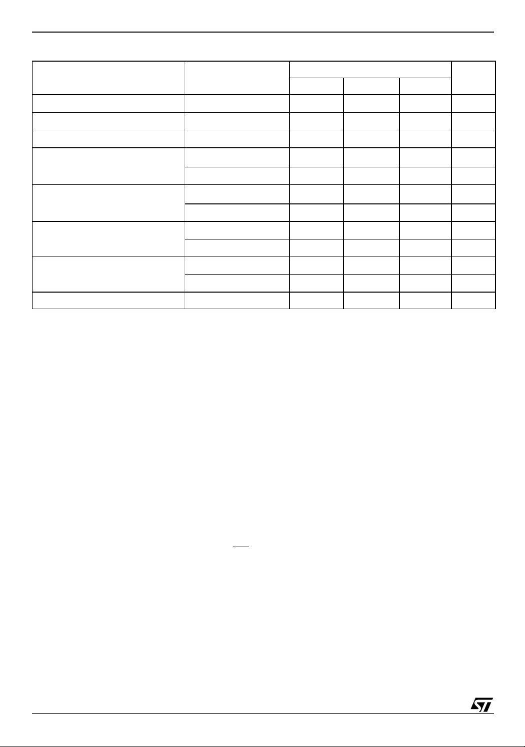
Table 8. Program, Erase Times and Program/Er ase Endu rance Cycles . . . . . . . . . . . . . . . . . . . . 16
BLOCK LOCKING. . . . . . . . . . . . . . . . . . . . . . . . . . . . . . . . . . . . . . . . . . . . . . . . . . . . . . . . . . . . . . . . . 16
Locked State . . . . . . . . . . . . . . . . . . . . . . . . . . . . . . . . . . . . . . . . . . . . . . . . . . . . . . . . . . . . . . . . . . 16
Unlocked State . . . . . . . . . . . . . . . . . . . . . . . . . . . . . . . . . . . . . . . . . . . . . . . . . . . . . . . . . . . . . . . . 16
Lock-Down State. . . . . . . . . . . . . . . . . . . . . . . . . . . . . . . . . . . . . . . . . . . . . . . . . . . . . . . . . . . . . . . 17
Reading a Block’s Lock Status . . . . . . . . . . . . . . . . . . . . . . . . . . . . . . . . . . . . . . . . . . . . . . . . . . . . 16
Locking Operations During Erase Suspend . . . . . . . . . . . . . . . . . . . . . . . . . . . . . . . . . . . . . . . . . . 17
Table 9. Block Lock Status . . . . . . . . . . . . . . . . . . . . . . . . . . . . . . . . . . . . . . . . . . . . . . . . . . . . . . . 17
Table 10. Protection Status . . . . . . . . . . . . . . . . . . . . . . . . . . . . . . . . . . . . . . . . . . . . . . . . . . . . . . . 18
STATUS REGISTER. . . . . . . . . . . . . . . . . . . . . . . . . . . . . . . . . . . . . . . . . . . . . . . . . . . . . . . . . . . . . . . 19
Program/Erase Controller Status (Bit 7) . . . . . . . . . . . . . . . . . . . . . . . . . . . . . . . . . . . . . . . . . . . . .19
Erase Suspend Status (Bit 6) . . . . . . . . . . . . . . . . . . . . . . . . . . . . . . . . . . . . . . . . . . . . . . . . . . . . . 19
Erase Status (Bit 5). . . . . . . . . . . . . . . . . . . . . . . . . . . . . . . . . . . . . . . . . . . . . . . . . . . . . . . . . . . . . 19
Program Status (Bit 4). . . . . . . . . . . . . . . . . . . . . . . . . . . . . . . . . . . . . . . . . . . . . . . . . . . . . . . . . . . 19
V
Status (Bit 3). . . . . . . . . . . . . . . . . . . . . . . . . . . . . . . . . . . . . . . . . . . . . . . . . . . . . . . . . . . . . . . 19
PP
Program Suspend Status (Bit 2) . . . . . . . . . . . . . . . . . . . . . . . . . . . . . . . . . . . . . . . . . . . . . . . . . . . 19
Block Protection Status (Bit 1). . . . . . . . . . . . . . . . . . . . . . . . . . . . . . . . . . . . . . . . . . . . . . . . . . . . . 20
Reserved (Bit 0). . . . . . . . . . . . . . . . . . . . . . . . . . . . . . . . . . . . . . . . . . . . . . . . . . . . . . . . . . . . . . . . 20
Table 11. Status Register Bits. . . . . . . . . . . . . . . . . . . . . . . . . . . . . . . . . . . . . . . . . . . . . . . . . . . . . 20
MAXIMUM RATING. . . . . . . . . . . . . . . . . . . . . . . . . . . . . . . . . . . . . . . . . . . . . . . . . . . . . . . . . . . . . . . . 21
Table 12. Absolute Maximum Ratings . . . . . . . . . . . . . . . . . . . . . . . . . . . . . . . . . . . . . . . . . . . . . . . 21
DC and AC PARAMETERS . . . . . . . . . . . . . . . . . . . . . . . . . . . . . . . . . . . . . . . . . . . . . . . . . . . . . . . . . 2 2
Table 13. Operating and AC Measurement Conditions. . . . . . . . . . . . . . . . . . . . . . . . . . . . . . . . . . 22
Figure 7. AC Measurement I/O Waveform . . . . . . . . . . . . . . . . . . . . . . . . . . . . . . . . . . . . . . . . . . .22
Figure 8. AC Measurement Load Circuit . . . . . . . . . . . . . . . . . . . . . . . . . . . . . . . . . . . . . . . . . . . . . 22
Table 14. Capacitance. . . . . . . . . . . . . . . . . . . . . . . . . . . . . . . . . . . . . . . . . . . . . . . . . . . . . . . . . . . 22
Table 15. DC Characteristics. . . . . . . . . . . . . . . . . . . . . . . . . . . . . . . . . . . . . . . . . . . . . . . . . . . . . . 23
Figure 9. Read AC Waveforms . . . . . . . . . . . . . . . . . . . . . . . . . . . . . . . . . . . . . . . . . . . . . . . . . . . . 24
Table 16. Read AC Characteristics . . . . . . . . . . . . . . . . . . . . . . . . . . . . . . . . . . . . . . . . . . . . . . . . . 24
Figure 10. Write AC Waveforms, Write Enable Controlled . . . . . . . . . . . . . . . . . . . . . . . . . . . . . . . 25
Table 17. Write AC Characteristics, Write Enable Controlled . . . . . . . . . . . . . . . . . . . . . . . . . . . . . 26
Figure 11. Write AC Waveforms, Chip Enable Controlled . . . . . . . . . . . . . . . . . . . . . . . . . . . . . . . . 27
Table 18. Write AC Characteristics, Chip Enable Controlled . . . . . . . . . . . . . . . . . . . . . . . . . . . . . 28
Figure 12. Power-Up and Reset AC Waveforms. . . . . . . . . . . . . . . . . . . . . . . . . . . . . . . . . . . . . . . 29
Table 19. Power-Up and Reset AC Characteristics . . . . . . . . . . . . . . . . . . . . . . . . . . . . . . . . . . . . 29
3/55

M28W640ECT, M28W640ECB
PACKAGE MECHANICAL . . . . . . . . . . . . . . . . . . . . . . . . . . . . . . . . . . . . . . . . . . . . . . . . . . . . . . . . . . 30
Figure 13. TSOP48 - 48 lead Plastic Thin Small Outline, 12 x 20mm, Package Outline . . . . . . . . 30
Table 20. TSOP48 - 48 lead Plastic Thin Small Outline, 12 x 20mm, Package Mechanical Data . 30
Figure 14. TFBGA48 6.39x10.5m m - 8x6 ball array, 0.75mm pitch, Bottom View Package Out line31
Table 21. TFBGA48 6.39x10.5mm - 8x6 ball array, 0.75mm pitch, Package Mechanical Data . . . 31
Figure 15. TFBGA48 Daisy Chain - Package Connections (Top view through package) . . . . . . . . 32
Figure 16. TFBGA48 Daisy Chain - PCB Connections proposal (Top view through package). . . . 32
PART NUMBERING . . . . . . . . . . . . . . . . . . . . . . . . . . . . . . . . . . . . . . . . . . . . . . . . . . . . . . . . . . . . . . . 33
Table 22. Ordering Information Scheme . . . . . . . . . . . . . . . . . . . . . . . . . . . . . . . . . . . . . . . . . . . . .33
Table 23. Daisy Chain Ordering Scheme . . . . . . . . . . . . . . . . . . . . . . . . . . . . . . . . . . . . . . . . . . . . 34
APPENDIX A. BLOCK ADDRESS TABLES . . . . . . . . . . . . . . . . . . . . . . . . . . . . . . . . . . . . . . . . . . . . 35
Table 24. Top Boot Block Addresses, M28W640ECT. . . . . . . . . . . . . . . . . . . . . . . . . . . . . . . . . . . 35
Table 25. Bottom Boot Block Addresses, M28W640ECB. . . . . . . . . . . . . . . . . . . . . . . . . . . . . . . . 37
APPENDIX B. COMMON FLASH INTERFACE (CFI) . . . . . . . . . . . . . . . . . . . . . . . . . . . . . . . . . . . . . 39
Table 26. Query Structure Overview. . . . . . . . . . . . . . . . . . . . . . . . . . . . . . . . . . . . . . . . . . . . . . . .39
Table 27. CFI Query Identification String . . . . . . . . . . . . . . . . . . . . . . . . . . . . . . . . . . . . . . . . . . . .39
Table 28. CFI Query System Interface Information. . . . . . . . . . . . . . . . . . . . . . . . . . . . . . . . . . . . . 40
Table 29. Device Geometry Definition. . . . . . . . . . . . . . . . . . . . . . . . . . . . . . . . . . . . . . . . . . . . . . .41
Table 30. Primary Algorithm-Specific Extended Query Table . . . . . . . . . . . . . . . . . . . . . . . . . . . . . 42
Table 31. Security Code Area . . . . . . . . . . . . . . . . . . . . . . . . . . . . . . . . . . . . . . . . . . . . . . . . . . . . . 43
APPENDIX C. FLOWCHARTS AND PSEUDO CODES. . . . . . . . . . . . . . . . . . . . . . . . . . . . . . . . . . . . 44
Figure 17. Program Flowchart and Pseudo Code . . . . . . . . . . . . . . . . . . . . . . . . . . . . . . . . . . . . . . 44
Figure 18. Double Word Program Flowchart and Pseudo Code . . . . . . . . . . . . . . . . . . . . . . . . . . . 45
Figure 19. Quadruple Word Program Flowchart and Pseudo Code . . . . . . . . . . . . . . . . . . . . . . . . 46
Figure 20. Program Suspend & Resume Flowchart and Pseudo Code . . . . . . . . . . . . . . . . . . . . . 47
Figure 21. Erase Flowchart and Pseudo Code . . . . . . . . . . . . . . . . . . . . . . . . . . . . . . . . . . . . . . . . 48
Figure 22. Erase Suspend & Resume Flowchart and Pseudo Code. . . . . . . . . . . . . . . . . . . . . . . . 49
Figure 23. Locking Operations Flowchart and Pseudo Code . . . . . . . . . . . . . . . . . . . . . . . . . . . . . 50
APPENDIX D. COMMAND INTERFACE AND PROGRAM/ERASE CONTROLLER STATE . . . . . . . 52
Table 32. Write State Machine Current/Next, sheet 1 of 2.. . . . . . . . . . . . . . . . . . . . . . . . . . . . . . . 52
Table 33. Write State Machine Current/Next, sheet 2 of 2.. . . . . . . . . . . . . . . . . . . . . . . . . . . . . . . 53
REVISION HISTORY. . . . . . . . . . . . . . . . . . . . . . . . . . . . . . . . . . . . . . . . . . . . . . . . . . . . . . . . . . . . . . . 54
Table 34. Document Revision History . . . . . . . . . . . . . . . . . . . . . . . . . . . . . . . . . . . . . . . . . . . . . . .54
4/55
SUMMARY DESCRIPTION
The M28W640EC is a 64 Mbit (4 Mbit x 16) nonvolatile Flash memory that can b e erased electrically at block level and programmed in-s ystem on
a Word-by-Word basis using a 2.7V to 3.6V V
supply for the circuitry and a 1.65V to 3.6V V
DD
DDQ
supply for the Input/Output pins. An optional 12V
V
power supply is provided to speed up custom-
PP
er programming.
The device features an asymmetrical blocked ar-
chitecture. The M28W640EC ha s an array of 135
blocks: 8 Parameter Blocks of 4 KWord and 127
Main Blocks of 32 KWord. M28W640ECT has the
Parameter Blocks at the top of the memory address space while the M28W640ECB locates the
Parameter Blocks starting from the bottom. The
memory maps are shown in Figure 5, Block Addresses.
The M28W640EC features an instant, individual
block locking scheme that allo ws any block to be
locked or unlocked with no latency, enabling instant code and data protection. All blocks have
three levels of protection. They can be locked and
locked-down individually preventing any accidental programming or erasure. There is an additional
hardware protection against program and erase.
When V
PP
≤ V
all blocks are protected against
PPLK
program or erase. All blocks are locked at Power
Up.
Each block can be erased separately. Erase can
be suspended in order to perform either read or
program in any other block and then resumed.
Program can be s uspended to read data in any
other block and then resumed. Each block can be
programmed and erased over 100,000 cycles.
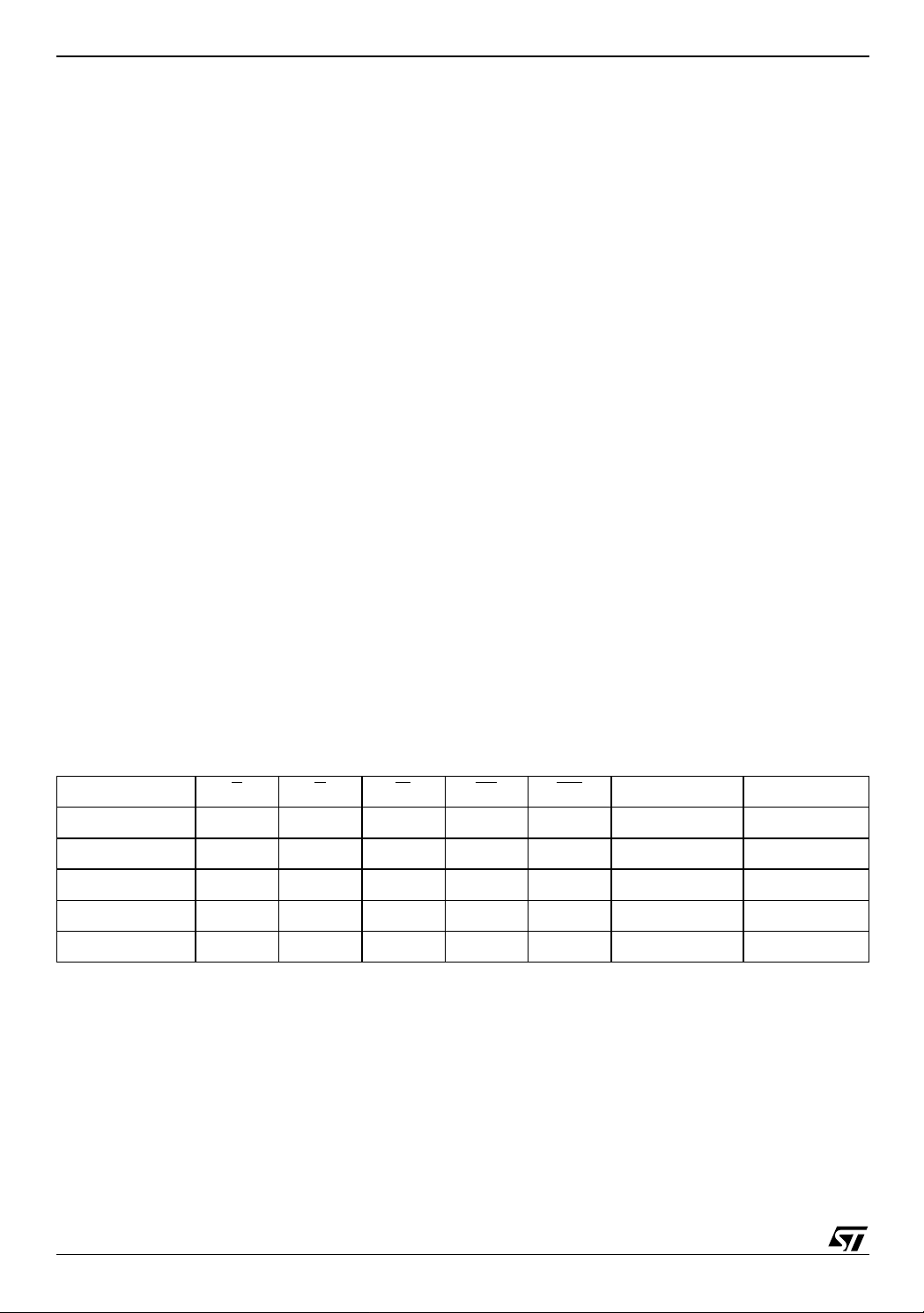
The device includes a 192 b it Protection Register
to increase th e pr o tection of a system design. The
Protection Register is divided into a 64 bit segment
and a 128 bit segment. The 64 bi t segment contains a unique device number written by ST, while
the second one is one-time-programmable by the
user. The user programmable segment can be
permanently protected. Figure 6, shows the Protection Register Memory Map.
Program and Erase command s are written to the
Command Interface of the memory. An on-chip
Program/Erase Controller takes care of the timings necessary for program and erase operations.
The end of a program or erase operation can be
detected and any error conditions identified. The
command set required to control the memory is
consistent with JEDEC standards.
M28W640ECT, M28W640ECB
The memory is of fered in TSOP48 (12 X 20mm)
and TFBGA48 (6.39 x 10.5mm, 0.75mm pitch)
packages and is supplied with all the bits erased
(set to ’1’).
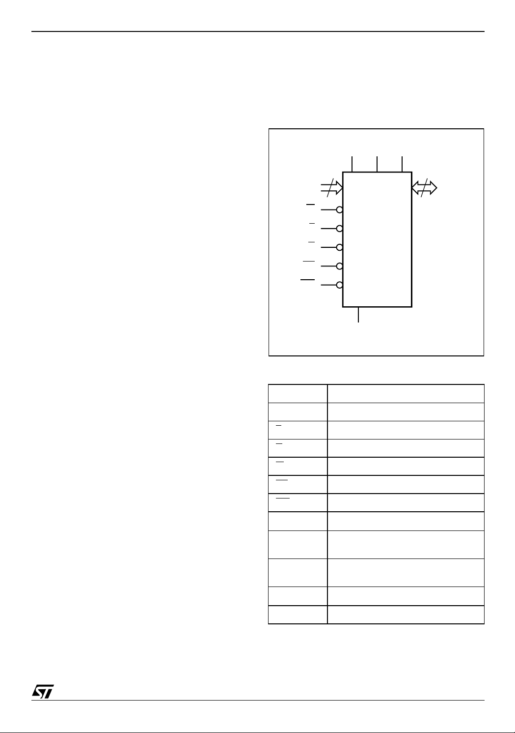
Figure 2. Logic Diagram
V
V
DD
DDQVPP
22
A0-A21
W
E
G
RP
WP
M28W640ECT
M28W640ECB
V
SS
Table 1. Signal Names
A0-A21 Address Inputs
DQ0-DQ15 Data Input/Output
E
G
W
RP
WP
V
DD
V
DDQ
V
PP
V
SS
NC Not Connected Internally
Chip Enable
Output Enable
Write Enable
Reset
Write Protect
Core Power Supply
Power Supply for
Input/Output
Optional Supply Voltage for
Fast Program & Erase
Ground
16
DQ0-DQ15
AI04378b
5/55
M28W640ECT, M28W640ECB
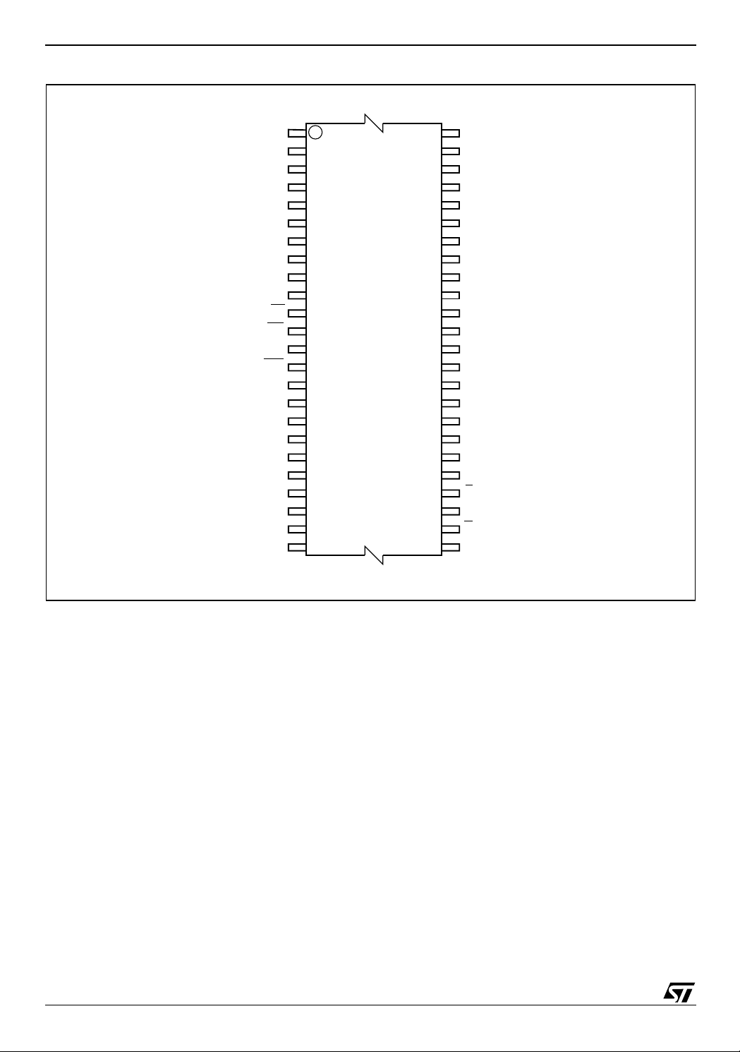
Figure 3. TSOP Connections
A15
A14
A13
A12
A11
1
48
A16
V
DDQ
V
SS
DQ15
DQ7
A10 DQ14
37
36
DQ6
DQ13
DQ5
DQ12
DQ4
V
DD
DQ11
DQ3
DQ10
DQ2
DQ9
DQ1
DQ8
DQ0
G
V
SS
E
A0
A21
A20
RP
V
PP
WP
A19
A18
A17
A9
A8
W
A7
A6
A5
A4
A3
A2
A1
12
M28W640ECT
M28W640ECB
13
24 25
AI04379b
6/55
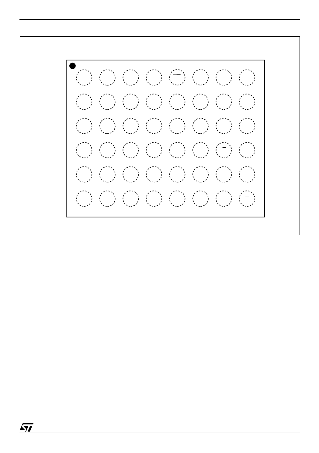
Figure 4. TFBGA Connections (Top view through package)
M28W640ECT, M28W640ECB
87654321
A
B
C
D
E
F
DDQ
SS
DQ7V
A8A11A13
DQ13
PP
RP A18
A21
DQ11
DQ12
DQ4
WP A19
A20
DQ2
DD
A7V
A5A17WA10A14
DQ0DQ9DQ3DQ6DQ15V
DQ1DQ10V
A4
A2
A1A3A6A9A12A15
A0EDQ8DQ5DQ14A16
V
SS
G
AI04380
7/55
M28W640ECT, M28W640ECB
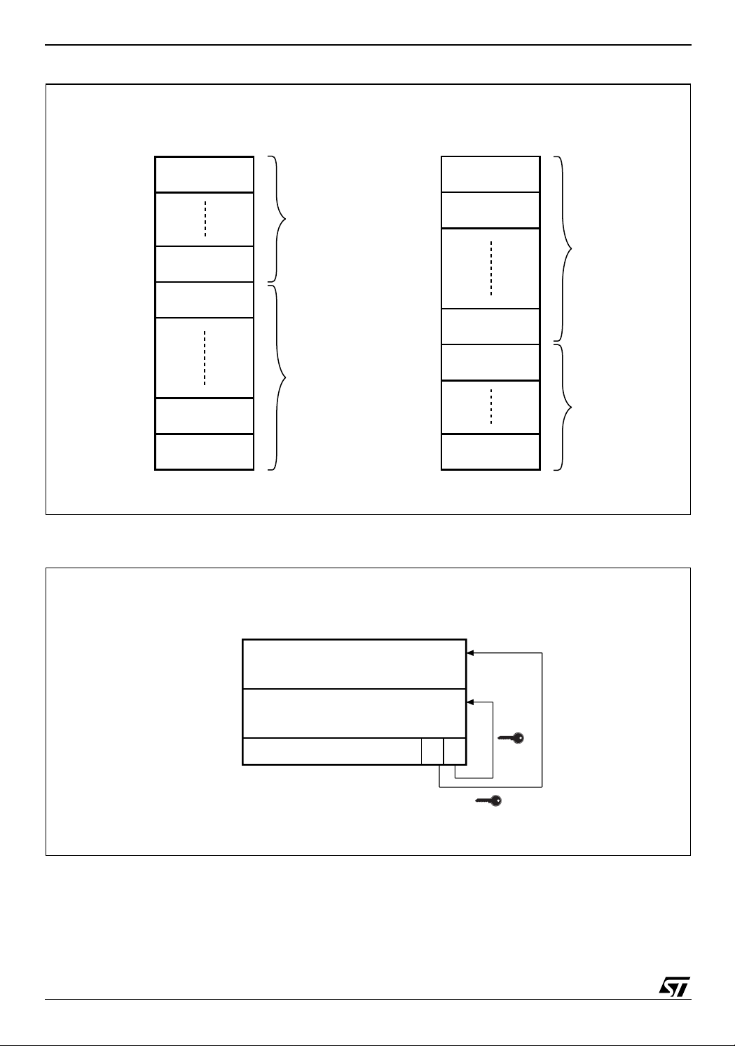
Figure 5. Block Addresses
M28W640ECT
Top Boot Block Addresses
3FFFFF
3FF000
3F8FFF
3F8000
3F7FFF
3F0000
00FFFF
008000
007FFF
000000
Note: A l so see Appe ndi x A, Tables 24 and 25 for a full l isting of the Bl ock Address es.
4 KWords
Total of 8
4 KWord Blocks
4 KWords
32 KWords
Total of 127
32 KWord Blocks
32 KWords
32 KWords
Bottom Boot Block Addresses
3FFFFF
3F8000
3F7FFF
3F0000
00FFFF
008000
007FFF
007000
000FFF
000000
M28W640ECB
32 KWords
32 KWords
Total of 127
32 KWord Blocks
32 KWords
4 KWords
Total of 8
4 KWord Blocks
4 KWords
AI04386b
Figure 6. Prot ect i on Register Me m o ry Map
PROTECTION REGISTER
8Ch
User Programmable OTP
85h
84h
81h
80h
Unique device number
Protection Register Lock 1 0
AI05520b
8/55

SIGNAL DESCRIPTIONS
See Figure 2 Logic Diagram and Table 1,Signal
Names, for a brief overview of the signals connected to this device.
Address Inputs (A0-A21). The Address Inputs select the cells i n the memory array to a ccess during Bus Read operations. During Bus Write operations they control the commands sent to the Command Interface of the internal state machine.
Data Input/Output (DQ0-DQ15). The Data I/O outputs the data stored at the selected address during a Bus Read operation or inputs a command or the data to be programmed durin g a Write Bus operation.
Chip Enable (E
). The Chip Enable input acti-
vates the memory control logic, input buffers, decoders and sense amplifiers. When Chip Enable is
and Reset is at VIH the device is in active
at V
IL
mode. When Chi p E nable i s at V
the memory is
IH
deselected, the outputs are high impedan ce and
the power consumption is reduced to the stand-by
level.
Output Enable (G
). The Output Enable controls
data outputs during the Bus Read operation of the
memory.
Write Enable (W
). The Write Enable controls the
Bus Write operation of the memory’s Command
Interface. The data and address inputs are latched
on the rising edge of Chip Enable, E, or Write Enable, W
Write Protect (WP
, whichever occurs first.
). Write Protect is an input
that gives an additional hardware protection for
each block. When Write Protect is at V
, the Loc k-
IL
Down is enabled and the prote ction status of t he
block cannot be changed. When Write Protect is at
, the Lock-Down is disabled and the block can
V
IH
be locked or unlocked. (refer to Table 7, Read Protection Register and Protection Register Lock).
Reset (RP
ware reset of the memory. W hen Reset is at V
). The Reset input provides a hard-
IL
the memory is in reset mode: the outputs are high
impedance and the current consumption is minimized. After Reset all blocks are in the Locked
M28W640ECT, M28W640ECB
state. When Reset is at V
operation. Exiting reset mode the device enters
read array mode, but a negative transition of Chip
Enable or a change of the addres s is required t o
ensure valid data outputs.
Supply Voltage. VDD provides the power
V
DD
supply to the internal core of the memory device.
It is the main power supply for all operations
(Read, Program and Erase).
Su pp ly V olt ag e . V
V
DDQ
power supply to the I/O pins a nd ena bles all Ou tputs to be powered independently from V
can be tied to VDD or can use a separate supply.
Program Supply Voltage. VPP is both a
V
PP
control input and a power supply pin. The two
functions are selected by the voltage range applied to the pin. The Supply Voltage V
Program Supply Voltage V
any order.
If V
is kept in a low voltage range (0V to 3.6V)
PP
V
is seen as a control input. In this case a volt-
PP
age lower than V
PPLK
against program or erase, whi le V
ables these functions (see Table 15, DC Characteristics for the relevant values). V
sampled at the beginning of a program or erase; a
change in its value after the operation has started
does not have any effect on Program or Erase,
however for Double or Q uadruple Word Program
the results are uncertain.
If V
is in the range 11.4V to 12.6V it acts as a
PP
power supply pin. In this condition V
stable until the Program/Erase algorit hm is completed (see Table 17 and 18).
Ground. VSS is the reference for all voltage
V
SS
measurements.
Note: Each device in a system should have
V
DD, VDDQ
pacitor close to the pin. See Figure 8, AC Mea-
,
and VPP decoupled wi th a 0.1 µF ca-
surement Load Circu it. The PCB trace widths
should be sufficient to carry the required V
program and erase currents.
, the device is in normal
IH
provides the
DDQ
can be applied in
PP
gives an absolute protection
PP
DD
and the
DD
> V
is only
PP
must be
PP
. V
PP1
DDQ
en-
PP
9/55
M28W640ECT, M28W640ECB
BUS OPERATIONS
There are six standard bus operations that control
the device. These are Bus Read, Bus Wri te, Output Disable, Standby, Automatic Standby and Reset. See Table 2, Bus Operations, for a summary.
Typically glitches of less than 5ns on Chip Enable
or Write Enable are ignored by the memory and do
not affect bus operations.
Read. Read Bus operations are used to output the contents of the Memory Array, the Electronic Signature, the Status Register and the Common Flash Interface. Both Chip Enable and Output Enable must be at V eration. The Chip Enable in put should be us ed to enable the device. Out put E nable shoul d be used to gate data onto the output. The data read depends on the previous command written to the memory (see Command Interface section). See Figure 9, Read Mode AC Wa veforms, and Table 16, Read AC Characteristics, for details of when the output becomes valid.
Read mode is the default state of the device when
exiting Reset or after power-up.
Write. Bus Write operations write Commands to the memory or latch Input Data to be programmed. A write operation is initiated when Chip Enable and Write Enable are at V V
. Commands, Input Data and Addresses are
IH
latched on the rising edge of Write Enable or Chip
Enable, whichever occurs first.
in order to perform a read op-
IL
with Output Enable at
IL
See Figures 10 and 11, Write AC Waveforms, and
Tables 17 and 18, Write AC Characteristics, for
details of the timing requirements.
Output Disa bl e . The data outputs are high impedance when the Output Enable is at V
.
IH
Standby. Stan dby disables most of the inte rnal circuitry allowing a substantial reduction of the current consumption. The memory is in stand-by when Chip Enable is at V
and the device is in
IH
read mode. The power consumption is reduced to
the stand-by level and the o utputs are set to high
impedance, independently from the Output Enable
or Write Enable inputs. If Chip Enable switches to
V
during a program or erase operation, t he de-
IH
vice enters Standby mode when finished. Automatic Standby. Automatic Standby pro-
vides a low power consumption state during Read
mode. Following a read operation, the device enters Automatic Standby after 150ns of bus inactivity even if Chip Enable is Low, V
current is reduced to I
. The data I nputs/Out-
DD1
, and the supply
IL
puts will still output data if a bus Read operation is
in progress.
Reset. During Reset mode when Output Enable is Low, V
, the memory is deselected and the out-
IL
puts are high impedance. The memory is in Reset
mode when Reset is at V
. The power consump-
IL
tion is reduced to the Standby level, independently
from the Chip Enable, Output Enable or Write Enable inputs. If Reset is pulled to V
during a Pro-
SS
gram or Erase, this operation is aborted and the
memory content is no longer valid.
Table 2. Bus Operations
Operation E G W RP WP
Bus Read
Bus Write
Output Disable
Standby
Reset X X X
Note: X = VIL or VIH, V
10/55
V
V
V
V
= 12V ± 5%.
PPH
IL
IL
IL
IH
V
IL
V
IH
V
IH
XX
V
IH
V
IL
V
IH
V
IH
V
IH
V
IH
V
IH
V
IL
V
PP
X Don’t Care Data Output
V
X
X Don’t Care Hi-Z
X Don’t Care Hi-Z
X Don’t Care Hi-Z
DD
or V
PPH
DQ0-DQ15
Data Input
COMMAND INTERFACE
All Bus Write operations t o the me mory are in terpreted by the Command Interface. Commands
consist of one or more sequential Bus Write operations. An internal Program/Erase Controller handles all timings and verifies the correct execution
of the Program and Erase commands. The Program/Erase Controller provides a S tatus Register
whose output may be read at any time during, to
monitor the progress of the operation, or the P rogram/Erase states. See Table 3, Command
Codes, for a summary o f the c ommands and see
Appendix 22, Table 32, Write State Machine Current/Next, for a summa ry of the Command Interface.
The Command Interface is reset to Read mode
when power is first applied, when exiting from Reset or whenever V
is lower than V
DD
LKO
. Command sequences must be followed exactly. Any
invalid combination of commands will reset the device to Read mode. Refer to Table 4, Commands,
in conjunction with the text descriptions below.
Read Memory Array Command
The Read command returns the memory to its
Read mode. One Bus Write cycle is required to issue the Read Memory Array command and return
the memory to Read mode. Subsequ ent read operations will read the addressed locat ion and output the data. When a device Reset occurs, the
memory defaults to Read mode.
Read Status Register Command
The Status Register indicates when a program or
erase operation is complete and the success or
failure of the operation itself. Issue a Read Status
Register command to rea d the Status Register’s
contents. Subsequent Bus Read op erations read
the Status Register at any address, u ntil another
command is issued. See Table 11, Status Register
Bits, for details on the definitions of the bits.
The Read Status Register command m ay be issued at any time, even during a Program/Erase
operation. Any Read attempt during a Program/
Erase operation will automatically output the content of the Status Register.
Read Electronic Signature Command
The Read Electronic Signature command reads
the Manufacturer and Device Codes and the Block
Locking Status, or the Protection Register.
The Read Electronic Signature command consists
of one write cycle, a subsequent read will output
the Manufacturer Code, the Device Code, the
Block Lock and Lock-Down Status, or the Protection and Lock Register. See Tables 5, 6 and 7 for
the valid address.
M28W640ECT, M28W640ECB
Table 3. Command Codes
Hex Code Command
01h Block Lock confirm
10h Program
20h Erase
2Fh Block Lock-Down confirm
30h
40h Program
50h Clear Status Register
56h
60h
70h Read Status Register
90h Read Electronic Signature
98h Read CFI Query
B0h Program/Erase Suspend
C0h Protection Register Program
D0h
FFh Read Memory Array
Read CFI Query Command
The Read Query Command is used to read dat a
from the Common Flash Interface (CFI) Me mory
Area, allowing programming equi pment or applications to automatically match their interface to
the characteristics of the device. One Bus Write
cycle is required to issue the Read Query Command. Once the command is issued subsequent
Bus Read operations read from the Common
Flash Interface Memory Area. See Appendix B,
Common Flash Inte rface, Tables 26, 27, 28, 29,
30 and 31 for details on the information contained
in the Common Flash Interface memory area.
Block Erase Command
The Block Erase com mand can be used to erase
a block. It sets all the bits within the selected block
to ’1’. All previous d ata in th e block is lost. If th e
block is protected then the Erase operation will
abort, the data in the block will not be changed and
the Status Register will output the error.
Two Bus Write cycles are required to issue the
command.
■ The first bus cycle sets up the Erase command.
Double Word Program
Quadruple Word Program
Block Lock, Block Unlock, Block Lock-
Down
Program/Erase Resume, Block Unlock
confirm
11/55

M28W640ECT, M28W640ECB
■ The second latches the block address in the
internal state machine and starts the Program/
Erase Controller.
If the second bus cycle is not Write Erase Confirm
(D0h), Status Register bits b4 and b5 a re s et and
the command aborts.
Erase aborts if Reset turns to V
. As data integrity
IL
cannot be guaranteed when the Erase operation is
aborted, the block must be erased again.
During Erase operations the memory will accept
the Read Status Re gister com mand and the P rogram/Erase Suspend command, all other commands will be ignored. Typical Erase times are
given in Table 8, Program, Erase Times and P rogram/Erase Endurance Cycles.
See Appendix C, Figure 21 , Erase Flowchart and
Pseudo Code, for a suggested flowchart for using
the Erase command.
Program Command
The memory array can be programmed word-byword. Two bus write cycles are required to issue
the Program Command.
■ The first bus cycle sets up the Program
command.
■ The second latches the Address and the Data to
be written and starts the Program/Erase
Controller.
During Program operations the memory will accept the Read Status Register command and the
Program/Erase Suspend command. Typical Program times are g iven in Tab le 8, P rogram, E rase
Times and Program/Erase Endurance Cycles.
Programming aborts if Reset goe s to V
. As data
IL
integrity cannot be guaranteed when the program
operation is aborted, the block containing the
memory location must be erased and reprogrammed.
See Appendix C, Figure 17, Program Flowchart
and Pseudo Code, for the f lowchart for using the
Program command.
Double Word Program Command
This feature is offered to improve the programming
throughput, writing a page of two adjacent words
in parallel.The two words m ust differ only for the
address A0. Programm ing should not be at t emp ted when V
is not at V
PP
PPH
.
Three bus write cycles are necessary to issue the
Double Word Program command.
■ The first bus cycle sets up the Double Word
Program Command.
■ The second bus cycle latches the Address and
the Data of the first word to be written.
■ The third bus cycle latches the Address and the
Data of the second word to be written and starts
the Program/Erase Controller.
Read operations output the Status Register content after the programming has s tarted. Programming aborts if Reset goes to V
. As data integrity
IL
cannot be guaranteed when the program operation is aborted, the block containing the memory
location must be erased and reprogrammed.
See Appendix C, Figure 18, Double Word Program Flowchart and Pseudo Code, for the flowchart for using the Double Word Program
command.
Quadruple Word Program Command
This feature is offered to improve the programming
throughput, writing a page of four adjacent words
in parallel.The four words must differ only for the
addresses A0 and A1. Programming should not be
attempted when V
is not at V
PP
PPH
.
Five bus write cycles are necessary to issue the
Quadruple Word Program command.
■ The first bus cycle sets up the Quadruple Word
Program Command.
■ The second bus cycle latches the Address and
the Data of the first word to be written.
■ The third bus cycle latches the Address and the
Data of the second word to be written.
■ The fourth bus cycle latches the Address and
the Data of the third word to be written.
■ The fifth bus cycl e latches the Addres s and th e
Data of the fourth word to be written and starts
the Program/Erase Controller.
Read operations output the Status Register content after the programming has s tarted. Programming aborts if Reset goes to V
. As data integrity
IL
cannot be guaranteed when the program operation is aborted, the block containing the memory
location must be erased and reprogrammed.
See Appendix C, Figure 19, Quadruple Word Program Flowchart and Pseudo Code, for the flowchart for using the Quadruple Word Program
command.
Clear Status Register Command
The Clear Status Register comm and c an b e us ed
to reset bits 1, 3, 4 and 5 in the Status Register to
‘0’. One bus write cycle is required to issue the
Clear Status Register command.
The bits in the Status Register do not automatically return to ‘0’ when a new Program or Erase command is issued. The error bits in the Status
Register should be cleared before attempting a
new Program or Erase command.
Program/Erase Suspend Command
The Program/Erase Suspend command is used to
pause a Program or Erase operation. One bus
write cycle is required to issue the Program/Erase
command and pau se the Prog ram/Erase controller.
12/55

M28W640ECT, M28W640ECB
During Program/Erase Suspend the Command Interface will accept the Program/Erase Resume,
Read Array, Read Status Register, Read Electronic Signature and Read CFI Query commands. Additionally, if the suspend operation was Erase then
the Program, Double Word Program, Quadruple
Word Program, Block Lock, Block Lock -Down or
Protection Program commands will also be accepted. The block being erased may be protected
by issuing the Block Protect, Block Lock or Protection Program commands. When the Program/
Erase Resume com mand is issued the operation
will complete. Only the blocks not being erased
may be read or programmed correctly.
During a Program/Erase Suspend, the device can
be placed in a pseudo-standby mode by taking
Chip Ena ble to V
Reset turns to V
. Program/Erase is aborted if
IH
.
IL
See Appendix C, Figure 20 , Program Suspend &
Resume Flowchart and Pseudo Code, and Figure
22, Erase Suspend & Resume Flowchart and
Pseudo Code for flowcharts for using the Program/
Erase Suspend command.
Program/Erase Resume Command
The Program/Erase Resume command can be
used to restart the Program/Erase Controller after
a Program/Erase Suspend o peration has paused
it. One Bus Write cycle is required to issue the
command. Once the command is issued subsequent Bus Read operations read the Status Register.
See Appendix C, Figure 20 , Program Suspend &
Resume Flowchart and Pseudo Code, and Figure
22, Erase Suspend & Resume Flowchart and
Pseudo Code for flowcharts for using the Program/
Erase Resume command.
Protectio n Register Program Command
The Protection Register Program command is
used to Program the 128 bit user O ne-Time-Programmable (OTP) segment of the Protection Register. The segment is programmed 16 bits at a
time. When shipped all bits in the segment are set
to ‘1’. The user can only program the bits to ‘0’.
Two write cycles are required to issue the Protec-
tion Register Program command.
■ The first bus cycle sets up the Protection
Register Program command.
■ The second latches the Address and the Data to
be written to the Protection Register and starts
the Program/Erase Controller.
Read operations output the Status Register content after the programming has started.
The segment can be protected by programming bit
1 of the Protection Lock Register (see F igure 6,
Protection Register Memory Map). Attempting to
program a previously prot ected Protection Regis-
ter will result in a Status Register error. The protection of the Protection Register is not reversible.
The Protection Register Program cannot be suspended.
Block Lock Command
The Block Lock command is used to lock a block
and prevent Program or Erase operations from
changing the data in it. All blocks are locked at
power-up or reset.
Two Bus Write cycles are required to issue the
Block Lock command.
■ The first bus cycle sets up the Block Lock
command.
■ The second Bus Write cycle latc hes the block
address.
The lock status can be monitored for each block
using the Read Electronic Signature command.
Table. 10 shows the protection status after issuing
a Block Lock command.
The Block Lock bits are vo latile, once set they remain set until a hardware reset or power-down/
power-up. They are cleared by a Blocks Unlock
command. Refer to the section, Block Locking, for
a detailed explanation.
Block Unlock Command
The Blocks Unlock command i s used to unlock a
block, allowing the block to be programmed or
erased. Two Bus Write cycles are requ ired to issue the Blocks Unlock command.
■ The first bus cycle sets up the Block Unlock
command.
■ The second Bus Write cycle latc hes the block
address.
The lock status can be monitored for each block
using the Read Electronic Signature command.
Table. 10 shows the protection status after issuing
a Block Unlock command. Refer to the section,
Block Locking, for a detailed explanation.
Block Lock-Down Command
A locked block cannot be Programmed or Erased,
or have its protection status changed when WP
low, V
. When WP is high, V
IL
the Lock-Down
IH,
is
function is disabled and the locked blocks can be
individually unlocked by the Block Unlock command.
Two Bus Write cycles are required to issue the
Block Lock-Down command.
■ The first bus cycle sets up the Block Lock
command.
■ The second Bus Write cycle latc hes the block
address.
The lock status can be monitored for each block
using the Read Electronic Signature command.
Locked-Down blocks revert to the locked (and not
13/55

M28W640ECT, M28W640ECB
locked-down) state when the device is reset on
power-down. Table. 10 sho ws the protection sta-
Refer to the section, Block Locking, for a detailed
explanation.
tus after issuing a Block Lock-Down command.
Table 4. Commands
Bus Write Operations
Commands
Read Memory
Array
Read Status
Register
Read Electronic
Signature
Read CFI Query 1+ Write X 98h Read QA QD
Erase 2 Write X 20h Write BA D0h
Program 2 Write X
Double Word
Program
Quadruple Word
Program
Clear Status
Register
Program/Erase
Suspend
Program/Erase
Resume
Block Loc k 2 Write X 60h Write
Block Unlock 2 Write X 60h Write
Block Loc k-Down 2 Write X 60h Write
Protection
Register Program
Note: 1. X = Don’t C are, RA=Rea d Addre ss, RD =Read D ata, SRD =Stat us Regis ter Da ta, ID =Identif ier (Ma nufact ure and Devic e Code),
(3)
(4)
QA=Query Address, QD=Query Data, BA=Block Address, PA=Program Address, PD=Program Data, PRA=Protection Register Address, PRD=Protection Register Data.
2. The s i gnature addresses are li st ed in Tables 5, 6 and 7.
3. Program Addres ses 1 and 2 must be consecuti ve Addresses differing only for A0.
4. Program Addres ses 1,2,3 and 4 m ust be consec utive Addr esses differi ng only for A 0 and A1.
5. To be c haracteriz ed.
1+ Write X FFh
1+ Write X 70h Read X SRD
1+ Write X 90h Read
1st Cycle 2nd Cycle 3rd Cycle 4th Cycle 5th Cycle
Cycles
Op. Add Data Op. Add Data Op. Add Data Op. Add Data Op. Add Data
RA RD
Read
(2)
IDh
SA
40h or
Write P A PD
10h
3 Write X 30h Write PA1 PD1 Write PA2 PD2
5 Write X
1 Write X 50h
1Write X B0h
1Write X D0h
(5)
Write PA1 PD1 Write PA2 PD2 Write PA3 PD3 Write PA4 PD4
56h
01h
BA
BA D0h
BA 2Fh
2 Write X C0h Write
PRA
PRD
Table 5. Read Electronic Signature
Code Device E G W A0 A1 A2-A7 A8-A21 DQ0-DQ7 DQ8-DQ15
Manufacture
Code
M28W640ECT
Device Code
M28W640ECB
Note: RP = VIH.
14/55
VILV
V
IL
V
VILV
IL
V
VILV
IL
V
IH
IHVIH
IHVIH
V
IL
V
V
0 Don’t Care 20h 00h
IL
0 Don’t Care 48h 88h
IL
0 Don’t Care 49h 88h
IL
M28W640ECT, M28W640ECB
Table 6. Read Block Lock Signature
Block Status E G W A0 A1 A2-A7 A8-A11 A12-A21 DQ0 DQ1 DQ2-DQ15
Locked Block
Unlocked Block
Locked-Down
Block
Note: 1. A Locked-Down Blo ck can be lock ed "DQ0 = 1" or unlocked "DQ0 = 0" ; s ee B l ock Locking section.
Table 7. Read Protection Register and Lock Register
Word E
Lock
Unique ID 0
Unique ID 1
Unique ID 2
Unique ID 3
OTP 0
OTP 1
OTP 2
OTP 3
OTP 4
OTP 5
OTP 6
OTP 7
V
ILVILVIHVILVIH
V
ILVILVIHVILVIH
V
ILVILVIHVILVIH
0 Don’t Care Block Address 1 0 00h
0 Don’t Care Block Address 0 0 00h
0 Don’t Care Block Address
X
(1)
1 00h
G W A0-A7 A8-A21 DQ0 DQ1 DQ2 DQ3-DQ7 DQ8-DQ15
V
ILVILVIH
V
ILVILVIH
V
ILVILVIH
V
ILVILVIH
V
ILVILVIH
V
ILVILVIH
V
ILVILVIH
V
ILVILVIH
V
ILVILVIH
V
ILVILVIH
V
ILVILVIH
V
ILVILVIH
V
ILVILVIH
80h Don’t Care 0
81h Don’t Care ID data ID data ID data ID data ID data
82h Don’t Care ID data ID data ID data ID data ID data
83h Don’t Care ID data ID data ID data ID data ID data
84h Don’t Care ID data ID data ID data ID data ID data
85h Don’t Care OTP data OTP data OTP data OTP data OTP data
86h Don’t Care OTP data OTP data OTP data OTP data OTP data
87h Don’t Care OTP data OTP data OTP data OTP data OTP data
88h Don’t Care OTP data OTP data OTP data OTP data OTP data
89h Don’t Care OTP data OTP data OTP data OTP data OTP data
8Ah Don’t Care OTP data OTP data OTP data OTP data OTP data
8Bh Don’t Care OTP data OTP data OTP data OTP data OTP data
8Ch Don’t Care OTP data OTP data OTP data OTP data OTP data
OTP Prot.
data
0 00h 00h
15/55
M28W640ECT, M28W640ECB
Table 8. Program , Erase Times and Program/Erase Endurance Cycl es
Parameter Test Conditions
V
Word Program
Double Word Program
Quadruple Word Program
Main Block Program
Parameter Block Program
Main Block Erase
Parameter Block Erase
Program/Erase Cycles (per Block) 100,000 cycles
Note: 1. Typical time to program a Main or Parameter Block using the Double Word Program and the Quadruple Word Program commands
respectively.
= V
PP
V
= 12V ±5%
PP
V
= 12V ±5%
PP
V
= 12V ±5%
PP
= V
V
PP
= 12V ±5%
V
PP
= V
V
PP
= 12V ±5%
V
PP
= V
V
PP
V
= 12V ±5%
PP
V
= V
PP
DD
DD
DD
DD
DD
Min Typ Max
M28W640EC
10 200 µs
10 200 µs
10 200 µs
0.16/0.08
0.02/0.01
(1)
0.32 5 s
(1)
0.04 4 s
110s
110s
0.4 10 s
0.4 10 s
5s
4s
Unit
BLOCK LOCKING
The M28W640EC features an instant, individual
block locking scheme that allo ws any block to be
locked or unlocked with no latency. This locking
scheme has three levels of protection.
■ Lock/Unlock - this first level allows software-
only control of block locking.
■ Lock-Down - this second level requires
hardware interaction before locking can be
changed.
■ V
PP
≤ V
- the third level offers a complete
PPLK
hardware protection against program and erase
on all blocks.
The protection status of each block can be set to
Locked, Unlocked, and Lock-Down. Table 10, defines all of the possible protection states (WP
DQ1, DQ0), and Appendi x C, Figure 23, shows a
flowchart for the locking operations.
Reading a Block’s Lock Status
The lock status of every block can be read in the
Read Electronic Signature mode of the device. To
enter this mode write 90h t o the device. Subsequent reads at the addres s specified in Table 6,
will output the pr otection sta tus of that bloc k. The
lock status is represented by DQ0 and DQ 1. DQ0
indicates the Block Lock/Unlock status and i s set
by the Lock comm and and cleared by the Unlock
command. It is also automatically set when entering Lock-Down. DQ1 indicates the Lock-Down status and is set by the Lock-Down command. It
cannot be cleared by software, only by a hardware
reset or power-down.
The following sections explain the operation of the
locking system.
Locked State
The default status of all blocks on power-up or after a hardware reset is L ocked (states (0,0,1) or
(1,0,1)). Locked blocks are fully protected from
any program or erase. Any program or erase operations attempted on a locked block will return an
error in the Status Register. The Status of a
Locked block can be changed to Unlocked or
Lock-Down using the appropriate software com-
,
mands. An Unlocked block can be Locked by issuing the Lock command.
Unlocked State
Unlocked blocks (states (0,0,0), (1,0,0) (1,1,0)),
can be programmed or erased. All unlocked
blocks return to the Locked state after a hardware
reset or when the device is powered-down. The
status of an unlocked block can be changed to
Locked or Locked-Down using the appropriate
software commands. A locked block can be unlocked by issuing the Unlock command.
16/55
M28W640ECT, M28W640ECB
Lock-Down State
Blocks that are Locked-Down (state (0,1,x))are
protected from program and erase operations (as
for Locked blocks) but th eir protect ion status cannot be changed using software comma nds alone.
A Locked or Unlocked block can be Locked-Down
by issuing the Lock-Down command. LockedDown blocks revert to the Locked state when the
device is reset or powered-down.
The Lock-Down function is depen dent on the WP
input pin. When WP=0 (VIL), the blocks in the
Lock-Down state (0,1,x) are protected from program, erase and protection status changes. When
=1 (VIH) the Lock-Down function is disabled
WP
(1,1,1) and Locked-Down blocks can be ind ividually unlocked to the (1,1,0) state by issuing the
software command, where they can be erased and
programmed. These blocks can then be relocked
(1,1,1) and unlocked (1,1,0) as desired while WP
remains high. When WP is low , blocks that were
previously Locked-Down return to the Lock-Down
state (0,1,x) regardless of any changes made
while WP
was high. Device reset or power-down
resets all blocks , including those in Lock-Down, to
the Locked state.
Locking Operations During Erase Suspend
Changes to block lock status can be performed
during an erase suspend by using the standard
locking command sequences to unlock, lock or
lock-down a block. This is useful in the case when
another block needs to be updated while an erase
operation is in progress.
To change block locking during an erase operation, first write the Erase Suspend command, then
check the status register until it indicates that the
erase operation has been suspended. Next write
the desired Lock com mand sequence to a block
and the lock status will be changed. After completing any desired lock, read, or program operations,
resume the erase operation with the Erase Resume command.
If a block is locked or locked-down during an erase
suspend of the same block, the locking status bits
will be changed immediately, b ut when the erase
is resumed, the erase operation will complete.
Locking operations cannot be performed du ring a
program suspend. Refer to Appendix D, Command Interface and Program/Erase Controller
State, for detailed information on which commands are valid during erase suspend.
Table 9. Block Lock Status
Item Address Data
Block Lock Configuration
Block is Unlocked DQ0=0
Block is Locked DQ0=1
Block is Locked-Down DQ1=1
LOCK
xx002
17/55

M28W640ECT, M28W640ECB
Table 10. Protection Status
Protection Status
(WP, DQ1, DQ0)
Current State
Current
Program/Erase
(1)
Allowed
After
Block Lock
Command
Next Protection Status
(WP, DQ1, DQ0)
After
Block Unlock
Command
1,0,0 yes 1,0,1 1,0,0 1,1,1 0,0,0
1,0,1
(2)
no 1,0,1 1,0,0 1,1,1 0,0,1
1,1,0 yes 1,1,1 1,1,0 1,1,1 0,1,1
1,1,1 no 1,1,1 1,1,0 1,1,1 0,1,1
0,0,0 yes 0,0,1 0,0,0 0,1,1 1,0,0
0,0,1
(2)
no 0,0,1 0,0,0 0,1,1 1,0,1
0,1,1 no 0,1,1 0,1,1 0,1,1
Note: 1. The lock status is defined by the write protect pin and by DQ1 (‘1’ for a locked-down block) and DQ0 (‘1’ for a locked block) as read
in the Read El ectronic Si gnature comm and with A1 = V
2. All blocks are locked at power -up, so the default config uration is 00 1 or 101 accor di ng to WP
3. A WP
transition to VIH on a locked block will restore the previous DQ0 value, giving a 111 or 110.
and A0 = VIL.
IH
(1)
After Block
Lock-Down
Command
status.
After
transition
WP
1,1,1 or 1,1,0
(3)
18/55

STATUS REGISTER
The Status Register provides information on the
current or previous Program or Erase operation.
The various bits convey information and errors on
the operation. To read the Status register the
Read Status Register command can be issued, refer to Read Status Register Command section. To
output the contents, the Status Register is latched
on the falling edge of the Chip Enable or Output
Enable signals, and can be read until Chip Enable
or Output Enable returns to V
. Either Chip En-
IH
able or Output Enable must be toggled to updat e
the latched data.
Bus Read operations from any address always
read the Status Register during Program and
Erase operations.
The bits in the Status Register are summarized in
Table 11, Status Register Bits. Refer to Table 11
in conjunction with the following text descriptions.
Program/Erase Controller Status (Bit 7). The Progra m/Erase Controller Status bit indicates whether
the Program/Erase Controller is active or inactive.
When the Program/Erase Controller Status bit is
Low (set to ‘0’), the Program/Erase Controller is
active; when the bit is High (set to ‘1’), the Program/Erase Controller is inactive, and the device
is ready to process a new command.
The Program/Erase Controller Status is Low immediately after a Program/Erase Suspend command is issued until the Program/Erase Controller
pauses. After the Program/Erase Controller pauses the bit is High .
During Program, Erase, o perations the Program/
Erase Controller Status bit can be polled to find the
end of the operation. Other bits in the Status Register should not be tested until the Program/Erase
Controller completes the operation and the bit is
High.
After the Program/Erase Cont roller completes its
operation the Erase Status, Prog ram Status, V
PP
Status and Block Lock Status bits should be tested
for errors.
Erase Suspend Status (Bit 6). The Erase Suspend Status bit indicates that an Erase o peration
has been suspended or is going to be suspended.
When the Erase Suspend Status bit is High (set to
‘1’), a Program/Erase Suspend command has
been issued and the memory is waiting for a Program/Erase Resume command.
The Erase Suspend Status should only be considered valid when the Program/Erase Controller Status bit is High (Program/Erase Controller inactive).
Bit 7 is set within 30µs of the Program/Erase Suspend command being issued therefore the memory may still complete the operation rather than
entering the Suspend mode.
M28W640ECT, M28W640ECB
When a Program/Erase Re sume command is issued the Erase Suspend Status bit returns Low.
Erase Status (Bit 5). The Erase Status bit can be
used to identify if the memory has failed to verify
that the block has erased correctly. When the
Erase Status bit is High (set to ‘1’), the Program/
Erase Controller has applied the m aximum number of pulses to the block and still failed to verify
that the block has erased correctly. The Erase Status bit should be read once the Program/Erase
Controller Status bit is High (Program/Erase Controller inactive).
Once set High, the Erase Status bit can only be reset Low by a Clear Status Register command or a
hardware reset. If set High it should be reset before a new Program or Erase command is issued,
otherwise the new command will appear to fail.
Program Status (Bit 4). The Program Status bit
is used to identify a Program failure. When the
Program Status bit is High (set to ‘1’), the Program/Erase Controller has applied the maximum
number of pulses to the byte and still failed to verify that it has programmed correctly. The Program
Status bit should be read once the Program/Erase
Controller Status bit is High (Program/Erase Controller inactive).
Once set High, the Program Status bit can only be
reset Low by a Clear Status Register command or
a hardware reset. If set High it should be reset before a new command is issued, otherwise the new
command will appear to fail.
Status (Bit 3). The VPP Status bit can be
V
PP
used to identify an invalid v oltage on the V
during Program and Erase operations. The V
pin is only sampled at the beginning of a Program
or Erase operation. Indeterminate results can occur if V
When the V
age on the V
when the V
becomes invalid during an operation.
PP
Status bit is Low (set to ‘0’), the volt-
PP
pin was sampled at a valid voltage;
PP
Status bit is High (set to ‘1’), the V
PP
pin has a voltage that is below the VPP Lockout
Voltage, V
, the memory is protected and Pro-
PPLK
gram and Erase operations cannot be performed.
Once set High, the V
Status bit can only be reset
PP
Low by a Clear Status Register command or a
hardware reset. If set High it should be reset before a new Program or Erase command is issued,
otherwise the new command will appear to fail.
Program Suspend Status (Bit 2). The Program
Suspend Status bit indicates that a Program operation has been suspended. When the Program
Suspend Status bit is High (set to ‘1’), a Program/
Erase Suspend command has been issued and
the memory is waiting for a Program/Erase Resume command. The Program Suspend Status
should only be considered valid when the Pro-
PP
pin
PP
PP
19/55

M28W640ECT, M28W640ECB
gram/Erase Controller Status bit is High (Program/
Erase Controller inactive). Bit 2 is set wi thin 5µs of
the Program/Erase Suspend comm and being issued therefore the memory may still complete t he
operation rather than entering the Suspend mode.
When a Program/Erase Re sume command is issued the Program Suspend Status bit returns Low.
Block Protection Status (Bit 1). The Block Protection Status bit can be used to identify if a Program or Erase operation has tried to modify the
contents of a locked block.
When the Block Protection Status bit is High (set
to ‘1’), a Program or Erase operation has been attempted on a locked block.
Once set High, the Block Protection Status bit can
only be reset Low by a Clear Status Register command or a hardware reset. If set High it should be
reset before a new command is issued, otherwise
the new command will appear to fail.
Reserved (Bit 0). Bit 0 of the Status Register is
reserved. Its value must be masked.
Note: Refer to Appendix C, Flowcharts and
Pseudo Codes, for using the Status Register.
Table 11. Status Register Bits
Bit Name Logic Level Definition
7 P/E.C. Status
6 Erase Suspend Status
5 Erase Status
4 Program Status
Status
3
2 Program Suspend Status
1 Block Protection Status
0 Reserved
Note: Logic level ’1’ is High, ’0’ is Low.
V
PP
’1’ Ready
’0’ Busy
’1’ Suspended
’0’ In progress or Completed
’1’ Erase Error
’0’ Erase Success
’1’ Program Error
’0’ Program Success
V
’1’
’0’
’1’ Suspended
’0’ In Progress or Completed
’1’ Program/Erase on protected Block, Abort
’0’ No operation to protected blocks
Invalid, Abort
PP
V
OK
PP
20/55

MAXIMUM RATIN G
Stressing the device ab ove the rating listed in t he
Absolute Maximum Ratings table m ay cause permanent damage to the device. These are stress
ratings only and operation of the device at these or
any other conditions ab ove those i ndicated in t he
Operating sections of this specificat ion is not im-
Table 12. Absolute Maximum Ratings
Symbol Parameter
T
A
T
BIAS
T
STG
V
IO
V
, V
DD
DDQ
V
PP
Note: 1. Depends on range.
Ambient Operating Temperature
Temperature Under Bias – 40 125 °C
Storage Temperature – 55 155 °C
Input or Output Voltage – 0.6
Supply Voltage – 0.6 4.1 V
Program Voltage – 0.6 13 V
(1)
M28W640ECT, M28W640ECB
plied. Exposure to Absolute Maximum Rating conditions for extended periods may affect device
reliability. Refer also to the STMicroelectronics
SURE Program and ot her relevant quality documents.
Value
Min Max
– 40 85 °C
V
+0.6
DDQ
Unit
V
21/55

M28W640ECT, M28W640ECB
DC AND AC PARAMETERS
This section summarizes the operat ing and measurement conditions, and the DC and AC characteristics of the device. The parameters in t he DC
and AC characteristics Tables that follow, are derived from tests performed under the Measure-
Table 13. Operating and AC Measurement Conditions
(1)
70
Min Max Min Max Min Max Min Max
3.0 3.6 3.0 3.6 2.7 3.6 2.7 3.6 V
V
Supply Voltage
DD
Parameter
ment Conditions summarized in Table 13,
Operating and AC Measurem ent Conditions. Designers should check that the operating conditions
in their circuit match the measurement conditions
when relying on the quoted parameters.
M28W640ECT, M28W640ECB
85 90 10
Units
Supply Voltage (V
V
DDQ
VDD)
DDQ
≤
1.65 3.6 1.65 3.6 1.65 3.6 1.65 3.6 V
Ambient Operating Temperature – 40 85 – 40 85 – 40 85 – 40 85 °C
Load Capacitance (C
)
L
50 50 50 50 pF
Input Rise and Fall Times 5 5 5 5 ns
Input Pulse Voltages
Input and Output Timing Ref.
Voltages
Note: 1. To be characterized.
0 to V
V
DDQ
DDQ
/2 V
0 to V
DDQ
DDQ
/2 V
0 to V
DDQ
DDQ
/2 V
0 to V
DDQ
DDQ
/2
Figure 7. AC Measurement I/O Waveform Figure 8. AC Measurement Load Circuit
V
DDQ
V
DDQ
V
/2
DDQ
0V
AI00610
V
DDQ
V
DD
25kΩ
DEVICE
UNDER
TEST
V
V
0.1µF
0.1µF
CL includes JIG capacitance
CL
Table 14. Capacitance
Symbol Parameter Test Condition Min Max Unit
V
V
IN
OUT
= 0V
= 0V
6pF
12 pF
C
IN
C
OUT
Note: Sampled only, not 10 0% tested.
Input Capacitance
Output Capacitance
22/55
25kΩ
AI00609C

M28W640ECT, M28W640ECB
Table 15. DC Characteristics
Symbol Parameter Test Condition Min Typ Max Unit
I
LI
I
LO
I
DD
I
DD1
I
DD2
I
DD3
I
DD4
I
DD5
I
PP
I
PP1
I
PP2
I
PP3
I
PP4
V
IL
V
IH
V
OL
V
OH
V
PP1
V
PPH
V
PPLK
V
LKO
Input Leakage Current
Output Leakage Current
Supply Current (Read)
Supply Current (Stand-by or
Automatic Stand-by)
Supply Current
(Reset)
Supply Current (Program)
Supply Current (Erase)
Supply Current
(Program/Erase Suspend)
Program Current
(Read or Stand-by)
Program Current
(Read or Stand-by)
Program Current (Reset)
Program Current (Program)
Program Current (Erase)
Input Low Voltage
Input High Voltage
Output Low Voltage
Output High Voltage
Program Voltage (Program or
Erase operations)
Program Voltage
(Program or Erase
operations)
Program Voltage
(Program and Erase lock-out)
VDD Supply Voltage (Program
and Erase lock-out)
0V≤ V
0V
E
= VSS, G = VIH, f = 5MHz
E
RP
RP
Program in progress
V
Program in progress
Erase in progress
V
Erase in progress
E
Erase suspended
RP
Program in progress
V
Program in progress
Erase in progress
V
Erase in progress
I
= 100µA, VDD = V
OL
V
I
= –100µA, VDD = V
OH
V
≤ V
IN
DDQ
V
≤
≤V
OUT
DDQ
= V
= V
DDQ
DDQ
± 0.2V,
± 0.2V
= VSS ± 0.2V
= 12V ± 5%
PP
V
= V
PP
DD
= 12V ± 5%
PP
V
= V
PP
DD
= V
V
V
DDQ
PP
PP
> V
≤ V
± 0.2V,
DD
DD
= VSS ± 0.2V
= 12V ± 5%
PP
= V
V
PP
DD
= 12V ± 5%
PP
= V
V
PP
DD
≥ 2.7V
V
DDQ
≥ 2.7V 0.7 V
V
DDQ
DDQ
DDQ
= V
= V
DDQ
DDQ
DD
min
DD
min
min,
min,
±1 µA
±10 µA
918mA
15 50 µA
15 50 µA
510mA
10 20 mA
520mA
10 20 mA
15 50 µA
400 µA
15µA
15µA
110mA
15µA
310mA
15µA
–0.5 0.4 V
–0.5 0.8 V
V
–0.4 V
DDQ
DDQ
V
DDQ
DDQ
+0.4
+0.4
0.1 V
–0.1
V
DDQ
1.65 3.6 V
11.4 12.6 V
1V
2V
V
V
V
23/55

M28W640ECT, M28W640ECB
Figure 9. Read AC Waveforms
tAVAV
A0-A21
tAVQV
E
tELQX
G
tGLQX
DQ0-DQ15
ADDR. VALID
CHIP ENABLE
Table 16. Read AC Characteristics
Symbol Alt Parameter
t
AVAV
t
AVQV
t
AXQX
t
EHQX
t
EHQZ
t
ELQV
t
ELQX
t
GHQX
t
GHQZ
t
GLQV
t
GLQX
Note: 1. Sampled only, not 100% tested.
2. G
3. To be c haracteriz ed.
t
Address Valid to Next Address Valid Min
RC
t
Address Valid to Output Valid Max
ACC
(1)
t
(1)
(1)
(2)
(1)
(1)
(1)
(2)
(1)
may be delayed by up to t
Address Transition to Output Transition Min 0 0 0 0 ns
OH
t
Chip Enable High to Output Transition Min 0 0 0 0 ns
OH
t
Chip Enable High to Output Hi-Z Max 20 20 25 25 ns
HZ
t
Chip Enable Low to Output Valid Max
CE
t
Chip Enable Low to Output Transition Min 0 0 0 0 ns
LZ
t
Output Enable High to Output Transition Min 0 0 0 0 ns
OH
t
Output Enable High to Output Hi-Z Max 20 20 25 25 ns
DF
t
Output Enable Low to Output Valid Max 20 20 30 30 ns
OE
t
Output Enable Low to Output Transition Min 0 0 0 0 ns
OLZ
ELQV
- t
after the fal ling edge of E without increasi ng t
GLQV
tELQV
tGLQV
OUTPUTS
ENABLED
VALID
VALID
DATA VALID STANDBY
M28W640EC
70 85 90 10
70
70
70
(3)
(3)
(3)
85 90 100 ns
85 90 100 ns
85 90 100 ns
ELQV
tAXQX
tEHQX
tEHQZ
tGHQX
tGHQZ
AI04387
Unit
.
24/55

Figure 10. Write AC Waveforms, Write Enable Controlled
M28W640ECT, M28W640ECB
AI04388
tWHAX
PROGRAM OR ERASE
tAVAV
VALIDA0-A21
tAVWH
tWHGL
tELQV
tWHEL
tQVWPL
STATUS REGISTER
tQVVPL
READ
1st POLLING
STATUS REGISTER
OR DATA INPUT
E
tELWL tWHEH
WP
tVPHWH
PP
V
SET-UP COMMAND CONFIRM COMMAND
tWPHWH
tWHWL
G
W
tWHDXtDVWH
tWLWH
DQ0-DQ15 COMMAND CMD or DATA
25/55

M28W640ECT, M28W640ECB
Table 17. Write AC Characteristics, Write Enable Controlled
Symbol A lt Parameter
t
AVAV
t
Write Cycle Time Min
WC
M28W640E C
70 85 90 10
70
(3)
85 90 100 ns
Unit
t
AVWH
t
DVWH
t
ELWL
t
ELQV
t
QVVPL
t
QVWPL
t
VPHWH
t
WHAX
t
WHDX
t
WHEH
t
WHEL
t
WHGL
t
WHWL
t
WLWH
t
WPHWH
Note: 1. Sampled only, not 100% tested.
2. Applicable if V
3. To be c haracteriz ed.
(1,2)
(1)
t
Address Valid to Write Enable High Min 45 45 50 50 ns
AS
t
Data Valid to Write Enable High Min 45 45 50 50 ns
DS
t
Chip Enable Low to Write Enable Low Min 0 0 0 0 ns
CS
Chip Enable Low to Output Valid Min
Output Valid to VPP Low
Output Valid to Write Protect Low Min 0 0 0 0 ns
t
VPSVPP
t
AH
t
DH
t
CH
High to Write Enable High
Write Enable High to Address Transition Min 0 0 0 0 ns
Write Enable High to Data Transition Min 0 0 0 0 ns
Write Enable High to Chip Enable High Min 0 0 0 0 ns
Write Enable High to Chip Enable Low Min 25 25 30 30 ns
Write Enable High to Output Enable Low Min 20 20 30 30 ns
t
Write Enable High to Write Enable Low Min 25 25 30 30 ns
WPH
t
Write Enable Low to Write Enable High Min 45 45 50 50 ns
WP
Write Protect High to Write Enable High Min 45 45 50 50 ns
is seen as a logic i nput (VPP < 3.6V ).
PP
70
(3)
85 90 100 ns
Min 0 0 0 0 ns
Min 200 2 00 200 200 ns
26/55

Figure 11. Write AC Waveforms, Chip Enable Controlled
M28W640ECT, M28W640ECB
AI04389
tEHAX
PROGRAM OR ERASE
tAVAV
VALIDA0-A21
tAVEH
tEHGL
tELQV
tQVWPL
CMD or DATA STATUS REGISTER
tQVVPL
READ
1st POLLING
STATUS REGISTER
OR DATA INPUT
CONFIRM COMMAND
W
tWLEL tEHWH
WP
tVPHEH
PP
V
POWER-UP AND
SET-UP COMMAND
tWPHEH
tEHEL
G
E
tEHDX
tELEH
tDVEH
DQ0-DQ15 COMMAND
27/55

M28W640ECT, M28W640ECB
Table 18. Write AC Characteristics, Chip Enable Controlled
Symbol Alt Parameter
t
AVAV
t
Write Cycle Time Min
WC
M28W640EC
70 85 90 10
70
(3)
85 90 100 ns
Unit
t
AVEH
t
DVEH
t
EHAX
t
EHDX
t
EHEL
t
EHGL
t
EHWH
t
ELEH
t
ELQV
(1,2)
t
QVVPL
t
QVWPL
t
VPHEH
t
WLEL
t
WPHEH
Note: 1. Sampled only, not 100% tested.
2. Applicable if V
3. To be c haracteriz ed.
(1)
t
Address Valid to Chip Enable High Min 45 45 50 50 ns
AS
t
Data Valid to Chip Enable High Min 45 45 50 50 ns
DS
Chip Enable High to Address
t
AH
Transition
t
Chip Enable High to Data Transition Min 0000ns
DH
t
Chip Enable High to Chip Enable Low Min 25 25 30 30 ns
CPH
Chip Enable High to Output Enable
Low
t
Chip Enable High to Write Enable High Min 0000ns
WH
t
Chip Enable Low to Chip Enable High Min 45 45 50 50 ns
CP
Chip Enable Low to Output Valid Min
Output Valid to VPP Low
Data Valid to Write Protect Low Min 0000ns
t
VPSVPP
t
CS
High to Chip Enable High
Write Enable Low to Chip Enable Low Min 0000ns
Write Protect High to Chip Enable High Min 45 45 50 50 ns
is seen as a logic i nput (VPP < 3.6V ).
PP
Min0000ns
Min 25 25 30 30 ns
70
(3)
85 90 100 ns
Min0000ns
Min 200 200 200 200 ns
28/55

Figure 12. Power-Up and Reset AC Waveforms
E, G
W,
RP
tPHWL
tPHEL
tPHGL
M28W640ECT, M28W640ECB
tPHWL
tPHEL
tPHGL
tVDHPH
VDD, VDDQ
Power-Up Reset
Table 19. Power-Up and Reset AC Characteristics
Symbol Parameter Test Condition
t
PHWL
t
PHEL
t
PHGL
t
PLPH
t
VDHPH
Note: 1. The de vice Reset is po ssible but not guarant eed if t
Reset High to Write Enable Low, Chip
Enable Low, Output Enable Low
(1,2)
Reset Low to Reset High Min 100 100 100 100 ns
(3)
Supply Voltages High to Reset High Min 50 50 50 50 µs
2. Sampled only, not 100% tested.
3. It is im portant to ass ert RP
in order to all ow proper CP U i ni tializat i on during pow er up or reset .
During Program
and Erase
others Min 30 30 30 30 ns
< 100ns.
PLPH
tPLPH
AI03537b
M28W640EC
Unit
70 85 90 10
Min 50 50 50 50 µs
29/55

M28W640ECT, M28W640ECB
PACKAGE MECHANICAL
Figure 13. TSOP48 - 48 lead Plastic Thin Small Outline, 12 x 20mm, Package Outline
A2
1 N
e
E
B
N/2
D1
D
DIE
A
CP
C
TSOP-a
Note: Drawing is not to scale.
LA1 α
Table 20. TSOP48 - 48 lead Plastic Thin Small Outline, 12 x 20mm, Package Mechanical Data
Symbol
Typ Min Max Typ Min Max
A 1.20 0.0472
A1 0.05 0.15 0.0020 0.0059
A2 0.95 1.05 0.0374 0.0413
B 0.17 0.27 0.0067 0.0106
C 0.10 0.2 1 0.0039 0.0083
D 19.80 20.20 0.7795 0.7953
D1 18.30 18.50 0.7205 0.7283
millimeters inches
E 11.90 12.10 0.4685 0.4764
e 0.50 – – 0.0197 – –
L 0.50 0.70 0.0 197 0.0279
α
N48 48
CP 0.10 0.0039
30/55
0° 5° 0° 5°

M28W640ECT, M28W640ECB
Figure 14. TFBGA48 6.39x10.5m m - 8x6 ball array, 0.75mm pitch, Bottom View Packa ge Outline
D
D1
FD
FE
E1E
BALL "A1"
A
Note: Drawing is not to scale.
SD
SE
e
ddd
e
b
A2
A1
BGA-Z34
Table 21. TFBGA48 6.39x10.5mm - 8x6 ball array, 0.75mm pitch, Package Mechanical Data
Symbol
Typ Min Max Typ Min Max
A 1.200 0.0472
A1 0.260 0.0102
millimeters inches
A2 1.000 0.0394
b 0.400 0.350 0.450 0.0157 0.0138 0.0177
D 6.390 6.290 6.490 0.2516 0.2476 0.2555
D1 5.250 – – 0.2067 – –
ddd 0.100 0.0039
E 10.500 10.400 10.600 0.4134 0.4094 0.4173
E1 3.750 – – 0.1476 – –
e 0.750 – – 0.0295 – –
FD 0.570 – – 0.0224 – –
FE 3.375 – – 0.1329 – –
SD 0.375 – – 0.0148 – –
SE 0.375 – – 0.0148 – –
31/55

M28W640ECT, M28W640ECB
Figure 15. TFBGA48 Daisy Chain - Package Connections (Top view through package)
87654321
A
B
C
D
E
F
AI04390
Figure 16. TFBGA48 Daisy Chain - PCB Connections proposal (Top view through package)
87654321
A
B
C
D
E
F
START
POINT
END
POINT
32/55
AI04391

M28W640ECT, M28W640ECB
PART NUMBERING
Table 22. Ordering Information Scheme
Example: M28W640ECT 90 N 6 T
Device Type
M28
Operating Voltage
W = V
Device Function
640EC = 64 Mbit (4 Mb x16), Boot Block
Array Matrix
T = Top Boot
B = Bottom Boot
Speed
70 = 70 ns (to be characterized)
85 = 85 ns
90 = 90 ns
10 = 100 ns
= 2.7V to 3.6V; V
DD
= 1.65V to 3.6V
DDQ
Package
N = TSOP48: 12 x 20 mm
ZB = TFBGA48: 6.39 x 10.5mm, 0.75 mm pitch
Temperature Range
1 = 0 to 70 °C
6 = –40 to 85 °C
Option
Blank = Standard Packing
T = Tape & Reel Packing
E = Lead-Free Package, Standard Packing
F = Lead-Free Package, Tape & Reel Packing
33/55

M28W640ECT, M28W640ECB
Table 23. Daisy Chain Ordering Scheme
Example: M28W640EC -ZB T
Device Type
M28W640EC
Daisy Chain
-ZB = TFBGA48: 6.39 x 10.5mm, 0.75 mm pitch
Option
Blank = Standard Packing
T = Tape & Reel Packing
E = Lead-Free Package, Standard Packing
F = Lead-Free Package, Tape & Reel Packing
Note:Devices are shipped from the factory with the memory content bits erased to ’1’. For a list of available
options (Speed, Package, etc...) or for further information on any aspect of this device, please contact
the ST Sales Office nearest to you.
34/55

APPENDIX A. BLOCK ADDRESS TABLES
M28W640ECT, M28W640ECB
Table 24. Top Boot Block Addresses, M28W640ECT
#
0 4 3FF000-3FFFFF
1 4 3FE000-3FEFFF
2 4 3FD000-3FDFFF
3 4 3FC000-3FCFFF
4 4 3FB000-3FBFFF
5 4 3FA000-3FAFFF
6 4 3F9000-3F9FFF
7 4 3F8000-3F8FFF
8 32 3F0000-3F7FFF
9 32 3E8000-3EFFFF
10 32 3E0000-3E7FFF
11 32 3D8000-3DFFFF
12 32 3D0000-3D7FFF
13 32 3C8000-3CFFFF
14 32 3C0000-3C7FFF
15 32 3B8000-3BFFFF
16 32 3B0000-3B7FFF
17 32 3A8000-3AFFFF
18 32 3A0000-3A7FFF
19 32 398000-39FFFF
20 32 390000-397FFF
21 32 388000-38FFFF
22 32 380000-387FFF
23 32 378000-37FFFF
24 32 370000-377FFF
25 32 368000-36FFFF
26 32 360000-367FFF
27 32 358000-35FFFF
28 32 350000-357FFF
29 32 348000-34FFFF
30 32 340000-347FFF
31 32 338000-33FFFF
32 32 330000-337FFF
33 32 328000-32FFFF
34 32 320000-327FFF
35 32 318000-31FFFF
36 32 310000-317FFF
37 32 308000-30FFFF
38 32 300000-307FFF
39 32 2F8000-2FFFFF
Size
(KWord)
Address Range
40 32 2F0000-2F7FFF
41 32 2E8000-2EFFFF
42 32 2E0000-2E7FFF
43 32 2D8000-2DFFFF
44 32 2D0000-2D7FFF
45 32 2C8000-2CFFFF
46 32 2C0000-2C7FFF
47 32 2B8000-2BFFFF
48 32 2B0000-2B7FFF
49 32 2A8000-2AFFFF
50 32 2A0000-2A7FFF
51 32 298000-29FFFF
52 32 290000-297FFF
53 32 288000-28FFFF
54 32 280000-287FFF
55 32 278000-27FFFF
56 32 270000-277FFF
57 32 268000-26FFFF
58 32 260000-267FFF
59 32 258000-25FFFF
60 32 250000-257FFF
61 32 248000-24FFFF
62 32 240000-247FFF
63 32 238000-23FFFF
64 32 230000-237FFF
65 32 228000-22FFFF
66 32 220000-227FFF
67 32 218000-21FFFF
68 32 210000-217FFF
69 32 208000-20FFFF
70 32 200000-207FFF
71 32 1F8000-1FFFFF
72 32 1F0000-1F7FFF
73 32 1E8000-1EFFFF
74 32 1E0000-1E7FFF
75 32 1D8000-1DFFFF
76 32 1D0000-1D7FFF
77 32 1C8000-1CFFFF
78 32 1C0000-1C7FFF
79 32 1B8000-1BFFFF
80 32 1B0000-1B7FFF
81 32 1A8000-1AFFFF
82 32 1A0000-1A7FFF
83 32 198000-19FFFF
35/55

M28W640ECT, M28W640ECB
84 32 190000-197FFF
85 32 188000-18FFFF
86 32 180000-187FFF
87 32 178000-17FFFF
88 32 170000-177FFF
89 32 168000-16FFFF
90 32 160000-167FFF
91 32 158000-15FFFF
92 32 150000-157FFF
93 32 148000-14FFFF
94 32 140000-147FFF
95 32 138000-13FFFF
96 32 130000-137FFF
97 32 128000-12FFFF
98 32 120000-127FFF
99 32 118000-11FFFF
100 32 110000-117FFF
101 32 108000-10FFFF
102 32 100000-107FFF
103 32 0F8000-0FFFFF
104 32 0F0000-0F7FFF
105 32 0E8000-0EFFFF
106 32 0E0000-0E7FFF
107 32 0D8000-0DFFFF
108 32 0D0000-0D7FFF
109 32 0C8000-0CFFFF
110 32 0C0000-0C7FFF
111 32 0B8000-0BFFFF
112 32 0B0000-0B7FFF
113 32 0A8000-0AFFFF
114 32 0A0000-0A7FFF
115 32 098000-09FFFF
116 32 090000-097FFF
117 32 088000-08FFFF
118 32 080000-087FFF
119 32 078000-07FFFF
120 32 070000-077FFF
121 32 068000-06FFFF
122 32 060000-067FFF
123 32 058000-05FFFF
124 32 050000-057FFF
125 32 048000-04FFFF
126 32 040000-047FFF
127 32 038000-03FFFF
128 32 030000-037FFF
129 32 028000-02FFFF
130 32 020000-027FFF
131 32 018000-01FFFF
132 32 010000-017FFF
133 32 008000-00FFFF
134 32 000000-007FFF
36/55

M28W640ECT, M28W640ECB
Table 25. Bottom Boot Block Addresses, M28W640ECB
#
134 32 3F8000-3FFFFF
133 32 3F0000-3F7FFF
132 32 3E8000-3EFFFF
131 32 3E0000-3E7FFF
130 32 3D8000-3DFFFF
129 32 3D0000-3D7FFF
128 32 3C8000-3CFFFF
127 32 3C0000-3C7FFF
126 32 3B8000-3BFFFF
125 32 3B0000-3B7FFF
124 32 3A8000-3AFFFF
123 32 3A0000-3A7FFF
122 32 398000-39FFFF
121 32 390000-397FFF
120 32 388000-38FFFF
119 32 380000-387FFF
118 32 378000-37FFFF
117 32 370000-377FFF
116 32 368000-36FFFF
115 32 360000-367FFF
114 32 358000-35FFFF
113 32 350000-357FFF
112 32 348000-34FFFF
111 32 340000-347FFF
110 32 338000-33FFFF
109 32 330000-337FFF
108 32 328000-32FFFF
107 32 320000-327FFF
106 32 318000-31FFFF
105 32 310000-317FFF
104 32 308000-30FFFF
103 32 300000-307FFF
102 32 2F8000-2FFFFF
101 32 2F0000-2F7FFF
100 32 2E8000-2EFFFF
99 32 2E0000-2E7FFF
98 32 2D8000-2DFFFF
97 32 2D0000-2D7FFF
96 32 2C8000-2CFFFF
95 32 2C0000-2C7FFF
94 32 2B8000-2BFFFF
93 32 2B0000-2B7FFF
Size
(KWord)
Address Range
92 32 2A8000-2AFFFF
91 32 2A0000-2A7FFF
90 32 298000-29FFFF
89 32 290000-297FFF
88 32 288000-28FFFF
87 32 280000-287FFF
86 32 278000-27FFFF
85 32 270000-277FFF
84 32 268000-26FFFF
83 32 260000-267FFF
82 32 258000-25FFFF
81 32 250000-257FFF
80 32 248000-24FFFF
79 32 240000-247FFF
78 32 238000-23FFFF
77 32 230000-237FFF
76 32 228000-22FFFF
75 32 220000-227FFF
74 32 218000-21FFFF
73 32 210000-217FFF
72 32 208000-20FFFF
71 32 200000-207FFF
70 32 1F8000-1FFFFF
69 32 1F0000-1F7FFF
68 32 1E8000-1EFFFF
67 32 1E0000-1E7FFF
66 32 1D8000-1DFFFF
65 32 1D0000-1D7FFF
64 32 1C8000-1CFFFF
63 32 1C0000-1C7FFF
62 32 1B8000-1BFFFF
61 32 1B0000-1B7FFF
60 32 1A8000-1AFFFF
59 32 1A0000-1A7FFF
58 32 198000-19FFFF
57 32 190000-197FFF
56 32 188000-18FFFF
55 32 180000-187FFF
54 32 178000-17FFFF
53 32 170000-177FFF
52 32 168000-16FFFF
51 32 160000-167FFF
50 32 158000-15FFFF
49 32 150000-157FFF
48 32 148000-14FFFF
47 32 140000-147FFF
37/55

M28W640ECT, M28W640ECB
46 32 138000-13FFFF
45 32 130000-137FFF
44 32 128000-12FFFF
43 32 120000-127FFF
42 32 118000-11FFFF
41 32 110000-117FFF
40 32 108000-10FFFF
39 32 100000-107FFF
38 32 0F8000-0FFFFF
37 32 0F0000-0F7FFF
36 32 0E8000-0EFFFF
35 32 0E0000-0E7FFF
34 32 0D8000-0DFFFF
33 32 0D0000-0D7FFF
32 32 0C8000-0CFFFF
31 32 0C0000-0C7FFF
30 32 0B8000-0BFFFF
29 32 0B0000-0B7FFF
28 32 0A8000-0AFFFF
27 32 0A0000-0A7FFF
26 32 098000-09FFFF
25 32 090000-097FFF
24 32 088000-08FFFF
23 32 080000-087FFF
22 32 078000-07FFFF
21 32 070000-077FFF
20 32 068000-06FFFF
19 32 060000-067FFF
18 32 058000-05FFFF
17 32 050000-057FFF
16 32 048000-04FFFF
15 32 040000-047FFF
14 32 038000-03FFFF
13 32 030000-037FFF
12 32 028000-02FFFF
11 32 020000-027FFF
10 32 018000-01FFFF
9 32 010000-017FFF
8 32 008000-00FFFF
7 4 007000-007FFF
6 4 006000-006FFF
5 4 005000-005FFF
4 4 004000-004FFF
3 4 003000-003FFF
2 4 002000-002FFF
1 4 001000-001FFF
0 4 000000-000FFF
38/55

M28W640ECT, M28W640ECB
APPENDIX B. COMMON FLASH INTERFACE (CFI)
The Common Flash Interface is a JEDEC approved, standardized data structure that can be
read from the Flash memory device. It allows a
system software to query the device to det ermine
various electrical and t iming parameters, density
information and functions supported by the memory. The system can interface easily with the device, enabling the software to upgrade itself when
necessary.
When the CFI Query Co mmand (RCFI) is issued
the device enters CFI Query mode and the data
Table 26. Query Structure Overview
Offset Sub-section Name Description
00h Reserved Reserved for algorithm-specific information
10h CFI Query Identification String Command set ID and algorithm data offset
1Bh System Interface Information Device timing & voltage information
27h Device Geometry Definition Flash device layout
P Primary Algorithm-specific Extended Query table
A Alternate Algorithm-specific Extended Query table
Note: Query data are always presented on the lowest order data outputs.
structure is read from the memory. Tables 26 , 27,
28, 29, 30 and 31 show the addresses used to retrieve the data.
The CFI data structure also contains a security
area where a 64 bit unique security number is written (see Table 31, Security Code area). This area
can be accessed only in Read mode by the final
user. It is impossible to change t he secu rity number after it has been written by ST. Issue a Read
command to return to Read mode.
Additional information specific to the Primary
Algorithm (optional)
Additional information specific to the Alternate
Algorithm (optional)
Table 27. CFI Query Identification String
Offset Data Description Value
00h 0020h Manufacturer Code ST
01h
02h-0Fh reserved Reserved
10h 0051h "Q"
11h 0052h Query Unique ASCII String "QRY" "R"
12h 0059h "Y"
13h 0003h
14h 0000h
15h 0035h
16h 0000h
17h 0000h
18h 0000h
19h 0000h
1Ah 0000h
Note: Query data are always presented on the lowest order data outputs (DQ7-DQ0) only. DQ8-DQ15 are ‘0’.
8848h
8849h
Device Code
Primary Algorithm Command Set and Control Interface ID code 16 bit ID code
defining a specific algorithm
Address for Primary Algorithm extended Query table (see Table 29) P = 35h
Alternate Vendor Command Set and Control Interface ID Code second vendor specified algorithm supported (0000h means none exists)
Address for Alternate Algorithm extended Query table
(0000h means none exists)
compatible
Top
Bottom
Intel
NA
NA
39/55

M28W640ECT, M28W640ECB
Table 28. CFI Query System Interface Information
Offset Data Description Value
V
Logic Supply Minimum Program/Erase or Write voltage
1Bh 0027h
1Ch 0036h
1Dh 00B4h
1Eh 00C6h
1Fh 0004h
20h 0004h
21h 000Ah
22h 0000h
23h 0005h
24h 0005h
25h 0003h
26h 0000h
DD
bit 7 to 4 BCD value in volts
bit 3 to 0 BCD value in 100 mV
Logic Supply Maximum Program/Erase or Write voltage
V
DD
bit 7 to 4 BCD value in volts
bit 3 to 0 BCD value in 100 mV
V
[Programming] Supply Minimum Program/Erase voltage
PP
bit 7 to 4 HEX value in volts
bit 3 to 0 BCD value in 100 mV
[Programming] Supply Maximum Program/Erase voltage
V
PP
bit 7 to 4 HEX value in volts
bit 3 to 0 BCD value in 100 mV
n
ms
n
times typical
n
µs
n
n
ms
Typical time-out per single word program = 2
Typical time-out for Double/Quadruple Word Program = 2
Typical time-out per individual block erase = 2
Typical time-out for full chip erase = 2
Maximum time-out for Word program = 2
Maximum time-out for Double/Quadruple Word Program = 2
Maximum time-out per individual block erase = 2
Maximum time-out for chip erase = 2
n
times typical
n
times typical
µs
n
times typical
2.7V
3.6V
11.4V
12.6V
16µs
16µs
1s
NA
512µs
512µs
8s
NA
40/55

Table 29. Device Geometry Definition
Offset Word
Mode
27h 0017h
28h
29h
2Ah
2Bh
2Ch 0002h
Data Description Value
Device Size = 2
0001h
0000h
0003h
0000h
Flash Device Interface Code description
Maximum number of bytes in multi-byte program or page = 2
Number of Erase Block Regions within the device.
It specifies the number of regions within the device containing contiguous
Erase Blocks of the same size.
n
in number of bytes
M28W640ECT, M28W640ECB
8 MByte
x16
Async.
n
8
2
2Dh
2Eh
2Fh
30h
31h
32h
M28W640ECT
33h
34h
2Dh
2Eh
2Fh
30h
31h
32h
M28W640ECB
33h
34h
007Eh
0000h
0000h
0001h
0007h
0000h
0020h
0000h
0007h
0000h
0020h
0000h
007Eh
0000h
0000h
0001h
Region 1 Information
Number of identical-size erase block = 007Eh+1
Region 1 Information
Block size in Region 1 = 0100h * 256 byte
Region 2 Information
Number of identical-size erase block = 0007h+1
Region 2 Information
Block size in Region 2 = 0020h * 256 byte
Region 1 Information
Number of identical-size erase block = 0007h+1
Region 1 Information
Block size in Region 1 = 0020h * 256 byte
Region 2 Information
Number of identical-size erase block = 007Eh=1
Region 2 Information
Block size in Region 2 = 0100h * 256 byte
127
64 KByte
8
8 KByte
8
8 KByte
127
64 KByte
41/55

M28W640ECT, M28W640ECB
Table 30. Primary Algorithm-Specific Extended Qu ery Ta bl e
Offset
P = 35h
(1)
Data Description Value
(P+0)h = 35h 0050h
(P+1)h = 36h 0052h "R"
Primary Algorithm extended Query table unique ASCII string “PRI”
"P"
(P+2)h = 37h 0049h "I"
(P+3)h = 38h 0031h Major version number, ASCII "1"
(P+4)h = 39h 0030h Minor version number, ASCII "0"
(P+5)h = 3Ah 0066h Extended Query table contents for Primary Algorithm. Address (P+5)h
(P+6)h = 3Bh 0000h
(P+7)h = 3Ch 0000h
(P+8)h = 3Dh 0000h
contains less significant byte.
bit 0 Chip Erase supported (1 = Yes, 0 = No)
bit 1 Suspend Erase supported (1 = Yes, 0 = No)
bit 2 Suspend Program supported (1 = Yes, 0 = No)
bit 3 Legacy Lock/Unlock supported (1 = Yes, 0 = No)
bit 4 Queued Erase supported (1 = Yes, 0 = No)
bit 5 Instant individual block locking supported (1 = Yes, 0 = No)
bit 6 Protection bits supported (1 = Yes, 0 = No)
bit 7 Page mode read supported (1 = Yes, 0 = No)
bit 8 Synchronous read supported (1 = Yes, 0 = No)
bit 31 to 9 Reserved; undefined bits are ‘0’
No
Yes
Yes
No
No
Yes
Yes
No
No
(P+9)h = 3Eh 0001h Supported Functions after Suspend
Read Array, Read Status Register and CFI Query are always supported
during Erase or Program operation
bit 0 Program supported after Erase Suspend (1 = Yes, 0 = No)
bit 7 to 1 Reserved; undefined bits are ‘0’ Yes
(P+A)h = 3Fh 0003h Block Lock Status
(P+B)h = 40h 0000h
Defines which bits in the Block Status Register section of the Query are
implemented.
Address (P+A)h contains less significant byte
bit 0 Block Lock Status Register Lock/Unlock bit active(1 = Yes, 0 = No)
bit 1 Block Lock Status Register Lock-Down bit active (1 = Yes, 0 = No)
Yes
Yes
bit 15 to 2 Reserved for future use; undefined bits are ‘0’
(P+C)h = 41h 0030h V
Logic Supply Optimum Program/Erase voltage (highest performance)
DD
3V
bit 7 to 4 HEX value in volts
bit 3 to 0 BCD value in 100 mV
(P+D)h = 42h 00C0h V
Supply Optimum Program/Erase voltage
PP
12V
bit 7 to 4 HEX value in volts
bit 3 to 0 BCD value in 100 mV
(P+E)h = 43h 0001h Number of Protection register fields in JEDEC ID space.
01
"00h," indicates that 256 protection bytes are available
(P+F)h = 44h 0080h Protection Field 1: Protection Description
(P+10)h = 45h 0000h 00h
(P+11)h = 46h 0003h 8 Byte
(P+12)h = 47h 0004h 16 Byte
This field describes user-available One Time Programmable (OTP)
Protection register bytes. Some are pre-programmed with device unique
serial numbers. Others are user programmable. Bits 0–15 point to the
Protection register Lock byte, the section’s first byte.
The following bytes are factory pre-programmed and user-programmable.
80h
bit 0 to 7 Lock/bytes JEDEC-plane physical low address
bit 8 to 15 Lock/bytes JEDEC-plane physical high address
bit 16 to 23 " n " such that 2n = factory pre-programmed bytes
n
bit 24 to 31 " n " such that 2
= user programmable bytes
(P+13)h = 48h Reserved
Note: 1. See Table 27, offset 15 for P pointer defin i tion.
42/55

Table 31. Security Code Area
Offset Data Description
80h 00XX Protection Register Lock
81h XXXX
82h XXXX
83h XXXX
84h XXXX
85h XXXX
86h XXXX
87h XXXX
88h XXXX
89h XXXX
8Ah XXXX
8Bh XXXX
8Ch XXXX
64 bits: unique device number
128 bits: User Programmable OTP
M28W640ECT, M28W640ECB
43/55

M28W640ECT, M28W640ECB
APPENDIX C. FLOWCHARTS AND PSEUDO CODES
Figure 17. Program Flow c hart and Pseudo Code
Start
Write 40h or 10h
Write Address
& Data
Read Status
Register
b7 = 1
YES
b3 = 0
YES
b4 = 0
YES
b1 = 0
YES
End
NO
NO
NO
NO
VPP Invalid
Error (1, 2)
Error (1, 2)
Program to Protected
Block Error (1, 2)
Program
program_command (addressToProgram, dataToProgram) {:
writeToFlash (any_address, 0x40) ;
/*or writeToFlash (any_address, 0x10) ; */
writeToFlash (addressToProgram, dataToProgram) ;
/*Memory enters read status state after
the Program Command*/
do {
status_register=readFlash (any_address) ;
/* E or G must be toggled*/
} while (status_register.b7== 0) ;
if (status_register.b3==1) /*VPP invalid error */
error_handler ( ) ;
if (status_register.b4==1) /*program error */
error_handler ( ) ;
if (status_register.b1==1) /*program to protect block error */
error_handler ( ) ;
}
AI03538b
Note: 1. Status check of b1 (Protected Blo ck), b3 (VPP Invalid) and b4 (P rogram Error) can be made af t er each program ope ration or afte r
a sequence.
2. If an er ror is found, the Status Register m ust be cleared before fu rt her Program / Erase Controller operations.
44/55

Figure 18. Dou bl e W or d Pr ogram Flowc hart and Pseudo Code
Start
M28W640ECT, M28W640ECB
Write 30h
Write Address 1
& Data 1 (3)
Write Address 2
& Data 2 (3)
Read Status
Register
b7 = 1
YES
b3 = 0
YES
b4 = 0
NO
NO
NO
VPP Invalid
Error (1, 2)
Program
Error (1, 2)
double_word_program_command (addressToProgram1, dataToProgram1,
addressToProgram2, dataToProgram2)
{
writeToFlash (any_address, 0x30) ;
writeToFlash (addressToProgram1, dataToProgram1) ;
/*see note (3) */
writeToFlash (addressToProgram2, dataToProgram2) ;
/*see note (3) */
/*Memory enters read status state after
the Program command*/
do {
status_register=readFlash (any_address) ;
/* E or G must be toggled*/
} while (status_register.b7== 0) ;
if (status_register.b3==1) /*VPP invalid error */
error_handler ( ) ;
if (status_register.b4==1) /*program error */
error_handler ( ) ;
YES
NO
b1 = 0
YES
End
Note: 1. Status check of b1 (Protected Blo ck), b3 (VPP Invalid) and b4 (P rogram Error) can be made af t er each program ope ration or afte r
a sequence.
2. If an er ror is found, the Status Register m ust be cleared before fu rt her Program / Erase operations.
3. Address 1 and Address 2 must be consecuti ve addresse s differing only for bit A0.
Program to Protected
Block Error (1, 2)
if (status_register.b1==1) /*program to protect block error */
error_handler ( ) ;
}
AI03539b
45/55
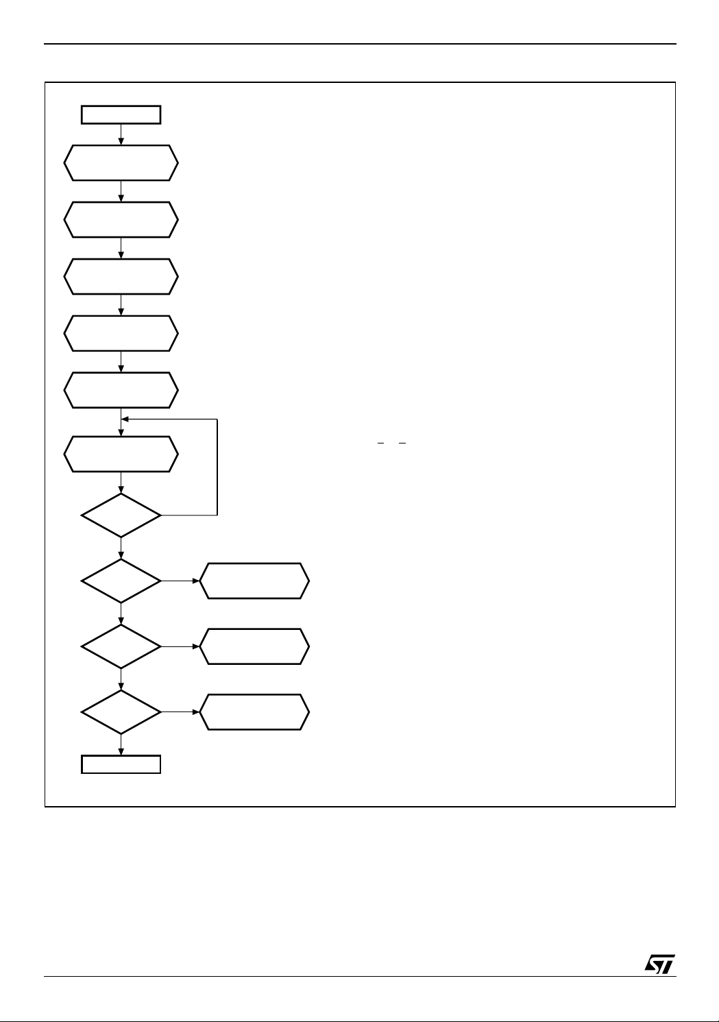
M28W640ECT, M28W640ECB
Figure 19. Qua dr upl e Word Program Fl owchart and Pse ud o C ode
Start
Write 56h
Write Address 1
& Data 1 (3)
Write Address 2
& Data 2 (3)
Write Address 3
& Data 3 (3)
Write Address 4
& Data 4 (3)
Read Status
Register
b7 = 1
YES
quadruple_word_program_command (addressToProgram1, dataToProgram1,
addressToProgram2, dataToProgram2,
addressToProgram3, dataToProgram3,
addressToProgram4, dataToProgram4)
{
writeToFlash (any_address, 0x56) ;
writeToFlash (addressToProgram1, dataToProgram1) ;
/*see note (3) */
writeToFlash (addressToProgram2, dataToProgram2) ;
/*see note (3) */
writeToFlash (addressToProgram3, dataToProgram3) ;
/*see note (3) */
writeToFlash (addressToProgram4, dataToProgram4) ;
/*see note (3) */
/*Memory enters read status state after
the Program command*/
do {
status_register=readFlash (any_address) ;
/* E or G must be toggled*/
NO
} while (status_register.b7== 0) ;
b3 = 0
b4 = 0
b1 = 0
End
Note: 1. Status check of b1 (Protected Blo ck), b3 (VPP Invalid) and b4 (P rogram Error) can be made af t er each program ope ration or afte r
a sequence.
2. If an er ror is found, the Status Register m ust be cleared before fu rt her Program / Erase operations.
3. Address 1 to Addr ess 4 must be consecutive addresses dif fering only for bits A0 and A1.
NO
YES
NO
YES
NO
YES
VPP Invalid
Error (1, 2)
Program
Error (1, 2)
Program to Protected
Block Error (1, 2)
if (status_register.b3==1) /*VPP invalid error */
error_handler ( ) ;
if (status_register.b4==1) /*program error */
error_handler ( ) ;
if (status_register.b1==1) /*program to protect block error */
error_handler ( ) ;
}
AI06233
46/55

M28W640ECT, M28W640ECB
Figure 20. Program Suspend & Resume Flowchart and Pseudo Code
Start
program_suspend_command ( ) {
Write B0h
Write 70h
Read Status
Register
writeToFlash (any_address, 0xB0) ;
writeToFlash (any_address, 0x70) ;
/* read status register to check if
program has already completed */
do {
status_register=readFlash (any_address) ;
/* E or G must be toggled*/
b7 = 1
YES
b2 = 1
YES
Write FFh
Read data from
another address
Write D0h
Program Continues
NO
NO
Program Complete
Write FFh
Read Data
} while (status_register.b7== 0) ;
if (status_register.b2==0) /*program completed */
{ writeToFlash (any_address, 0xFF) ;
read_data ( ) ; /*read data from another block*/
/*The device returns to Read Array
(as if program/erase suspend was not issued).*/
}
else
{ writeToFlash (any_address, 0xFF) ;
read_data ( ); /*read data from another address*/
writeToFlash (any_address, 0xD0) ;
/*write 0xD0 to resume program*/
}
}
AI03540b
47/55

M28W640ECT, M28W640ECB
Figure 21. Erase Flowchart and Pseudo Code
Start
Write 20h
Write Block
Address & D0h
erase_command ( blockToErase ) {
writeToFlash (any_address, 0x20) ;
writeToFlash (blockToErase, 0xD0) ;
/* only A12-A20 are significannt */
/* Memory enters read status state after
the Erase Command */
Read Status
Register
YES
YES
NO
YES
YES
NO
NO
YES
NO
NO
VPP Invalid
Error (1)
Command
Sequence Error (1)
Erase to Protected
Block Error (1)
b7 = 1
b3 = 0
b4, b5 = 1
b5 = 0 Erase Error (1)
b1 = 0
End
do {
status_register=readFlash (any_address) ;
/* E or G must be toggled*/
} while (status_register.b7== 0) ;
if (status_register.b3==1) /*VPP invalid error */
error_handler ( ) ;
if ( (status_register.b4==1) && (status_register.b5==1) )
/* command sequence error */
error_handler ( ) ;
if ( (status_register.b5==1) )
/* erase error */
error_handler ( ) ;
if (status_register.b1==1) /*program to protect block error */
error_handler ( ) ;
}
AI03541b
Note: I f an error is fo und, the Status Register mu st be cleared b ef ore further Pr ogram/Eras e operations.
48/55

Figure 22. Erase Suspend & Resume Flowchart and Pseudo Code
Start
M28W640ECT, M28W640ECB
Write B0h
Write 70h
Read Status
Register
b7 = 1
b6 = 1
Write FFh
Read data from
another block
Program/Protection Program
Block Protect/Unprotect/Lock
or
or
Write D0h
Erase Continues
NO
YES
NO
YES
Erase Complete
Write FFh
Read Data
erase_suspend_command ( ) {
writeToFlash (any_address, 0xB0) ;
writeToFlash (any_address, 0x70) ;
/* read status register to check if
erase has already completed */
do {
status_register=readFlash (any_address) ;
/* E or G must be toggled*/
} while (status_register.b7== 0) ;
if (status_register.b6==0) /*erase completed */
{ writeToFlash (any_address, 0xFF) ;
read_data ( ) ;
/*read data from another block*/
/*The device returns to Read Array
(as if program/erase suspend was not issued).*/
}
else
{ writeToFlash (any_address, 0xFF) ;
read_program_data ( );
/*read or program data from another address*/
writeToFlash (any_address, 0xD0) ;
/*write 0xD0 to resume erase*/
}
}
AI03542b
49/55

M28W640ECT, M28W640ECB
Figure 23. Lo ck i ng Ope rations Flowchart an d Pseudo Cod e
Start
Write 60h
Write
01h, D0h or 2Fh
Write 90h
Read Block
Lock States
Locking
change
confirmed?
YES
Write FFh
End
NO
locking_operation_command (address, lock_operation) {
writeToFlash (any_address, 0x60) ; /*configuration setup*/
if (lock_operation==LOCK) /*to protect the block*/
writeToFlash (address, 0x01) ;
else if (lock_operation==UNLOCK) /*to unprotect the block*/
writeToFlash (address, 0xD0) ;
else if (lock_operation==LOCK-DOWN) /*to lock the block*/
writeToFlash (address, 0x2F) ;
writeToFlash (any_address, 0x90) ;
if (readFlash (address) ! = locking_state_expected)
error_handler () ;
/*Check the locking state (see Read Block Signature table )*/
writeToFlash (any_address, 0xFF) ; /*Reset to Read Array mode*/
}
AI04364
50/55

M28W640ECT, M28W640ECB
Figure 24. Protection Register Program Flowchart and Pseudo Code
Start
Write C0h
Write Address
& Data
Read Status
Register
b7 = 1
YES
b3 = 0
YES
b4 = 0
YES
b1 = 0
YES
End
NO
NO
NO
NO
VPP Invalid
Error (1, 2)
Error (1, 2)
Program to Protected
Block Error (1, 2)
Program
protection_register_program_command (addressToProgram, dataToProgram) {:
writeToFlash (any_address, 0xC0) ;
writeToFlash (addressToProgram, dataToProgram) ;
/*Memory enters read status state after
the Program Command*/
do {
status_register=readFlash (any_address) ;
/* E or G must be toggled*/
} while (status_register.b7== 0) ;
if (status_register.b3==1) /*VPP invalid error */
error_handler ( ) ;
if (status_register.b4==1) /*program error */
error_handler ( ) ;
if (status_register.b1==1) /*program to protect block error */
error_handler ( ) ;
}
AI04381
Note: 1. Status check of b1 (Protected Blo ck), b3 (VPP Invalid) and b4 (P rogram Error) can be made af t er each program ope ration or afte r
a sequence.
2. If an er ror is found, the Status Register m ust be cleared before fu rt her Program / Erase Controller operations.
51/55

M28W640ECT, M28W640ECB
APPENDIX D. COMMAND INTERFACE AND PROGRAM/ERASE CONTROLLER STATE
Table 32. Write State Machine Current/Next, sheet 1 of 2.
Current
State
Read A rray “1” Array Read Array Prog. S e t up Ers. Setup Read Array Read Sts. Read Array
Read
Status
Read
Elect.Sg.
Read CFI
Query
Lock Setup “1” Status Lock Com mand Error
Lock Cmd
Error
Lock
(complete)
Prot. Prog.
Setup
Prot. Prog.
(continue)
Prot. Prog.
(complete)
Prog. Setup “1” Status Program
Program
(continue)
Prog. Sus
Status
Prog. Sus
Read A rray
Prog. Sus
Read
Elect.Sg.
Prog. Sus
Read CFI
Program
(complete)
Erase
Setup
Erase
Cmd.Error
Erase
(continue)
Erase Sus
Read Sts
Erase Sus
Read A rray
Erase Sus
Read
Elect.Sg.
Erase Sus
Read CFI
Erase
(complete)
Note: Cmd = Command, Elect.Sg. = Electronic Signature, Ers = Erase, Prog. = Pro gram , Prot = Protection, Sus = Suspend.
bit 7
Data
SR
When
Read
“1” Status Read Array
Electronic
“1”
Signature
“1” CFI Read Array
“1” Status Read Array
“1” Status Read Array
“1” Status Protec t i on Register P rogram
“0” Status Protecti on Register Program co ntinue
“1” Status Read Array
“0” Status Program (c ont i nue)
“1” Status
“1” Array
Electronic
“1”
Signature
“1” CFI
“1” Status Read Array
“1” Status Erase Command Error
“1” Status Read Array
“0” Status Erase (cont i nue)
“1” Status
“1” Array
Electronic
“1”
Signature
“1” CFI
“1” Status Read Array
Read
Array
(FFh)
Read Array
Prog. Sus
Read Array
Prog. Sus
Read Array
Prog. Sus
Read Array
Prog. Sus
Read Array
Erase Sus
Read Array
Erase Sus
Read Array
Erase Sus
Read Array
Erase Sus
Read Array
Program
Setup
(10/40h)
Program
Setup
Program
Setup
Program
Setup
Program
Setup
Program
Setup
Program
Setup
Program Suspend to
Read Array
Program Suspend to
Read Array
Program Suspend to
Read Array
Program Suspend to
Read Array
Program
Setup
Program
Setup
Program
Setup
Program
Setup
Program
Setup
Program
Setup
Program
Setup
Command Input (and Next State)
Erase
Setup
(20h)
Erase
Setup
Erase
Setup
Erase
Setup
Erase
Setup
Erase
Setup
Erase
Setup
Erase
Setup
Erase
Setup
Erase Sus
Read Array
Erase Sus
Read Array
Erase Sus
Read Array
Erase Sus
Read Array
Erase
Setup
Erase
Confirm
(D0h)
Lock
(complete)
Program
(continue)
Program
(continue)
Program
(continue)
Program
(continue)
Erase
(continue)
Erase
(continue)
Erase
(continue)
Erase
(continue)
Erase
(continue)
Prog/Ers
Suspend
(B0h)
Read Array
Read Array
Read Array
Lock Cmd
Error
Read Array
Read Array
Read Array
Prog. Sus
Read Sts
Prog. Sus
Read Array
Prog. Sus
Read Array
Prog. Sus
Read Array
Prog. Sus
Read Array
Read Array
Erase
CmdError
Read Array
Erase Sus
Read Sts
Erase Sus
Read Array
Erase Sus
Read Array
Erase Sus
Read Array
Erase Sus
Read Array
Read Array
Prog/Ers
Resume
(D0h)
Lock
(complete)
Program
(continu e)
Program
(continu e)
Program
(continu e)
Program
(continu e)
Erase
(continue)
Erase
(continu e)
Erase
(continu e)
Erase
(continu e)
Erase
(continu e)
Read
Status
(70h)
Read
Status
Read
Status
Read
Status
Lock Command Error
Read
Status
Read
Status
Read
Status
Program (c ontinue)
Prog. Sus
Read Sts
Prog. Sus
Read Sts
Prog. Sus
Read Sts
Prog. Sus
Read Sts
Read
Status
Erase Command Error
Read
Status
Erase (con tinue)
Eras e Sus
Read Sts
Eras e Sus
Read Sts
Eras e Sus
Read Sts
Eras e Sus
Read Sts
Read
Status
Clear
Status
(50h)
Read Array
Read Array
Read Array
Read Array
Read Array
Read Array
Prog. Sus
Read Array
Prog. Sus
Read Array
Prog. Sus
Read Array
Prog. Sus
Read Array
Read Array
Read Array
Eras e Sus
Read Array
Eras e Sus
Read Array
Eras e Sus
Read Array
Eras e Sus
Read Array
Read Array
52/55

M28W640ECT, M28W640ECB
Table 33. Write State Machine Current/Next, sheet 2 of 2.
Command Input (and Next State)
Current State
Read Array Read Elect.Sg. Read CFI Query Lock Setup
Read Status Read Elect.S g. Read CFI Query Lock S etup
Read Ele ct .Sg. Read Elect.Sg. Read CFI Query Lock Setup
Read CFI Query Read Elect.Sg. Read CFI Query Lock Setup
Lock S etup Lock Comma nd Error Loc k (complete)
Lock Cmd Error Read Elect.Sg. Read CFI Query Lock Setup
Lock (complete) Read Elect. Sg. Read CFI Query Lock Setup
Prot. Prog.
Setup
Prot. Prog.
(continue)
Prot. Prog.
(complete)
Prog. Setup Program
Program
(continu e)
Prog. Suspend
Read Status
Prog. Suspend
Read Array
Prog. Suspend
Read El ect.Sg.
Prog. Suspend
Read CFI
Program
(complete)
Erase Setup Erase Command Error
Erase
Cmd.Error
Erase (con tinue) Erase (continue)
Erase Suspend
Read Ststus
Erase Suspend
Read Array
Erase Suspend
Read El ect.Sg.
Erase Suspend
Read CFI Query
Erase
(complete)
Note: Cmd = Command, Elect.Sg. = Electronic Signature, Pro g. = Program, Pro t = P rot ection.
Read Elect.Sg.
(90h)
Read Elec t. S g. Read CFI Query Lo ck S et up
Prog. Suspend
Read Elec t.Sg.
Prog. Suspend
Read Elec t.Sg.
Prog. Suspend
Read Elec t.Sg.
Prog. Suspend
Read Elec t.Sg.
Read Elect.Sg. Read CFIQuery Lock Setup
Read Elec t. S g. Read CFI Query Lo ck S et up
Erase Suspend
Read Elec t.Sg.
Erase Suspend
Read Elec t.Sg.
Erase Suspend
Read Elec t.Sg.
Erase Suspend
Read Elec t.Sg.
Read Elec t.Sg. Read CFI Query Lock Setup
Read CFI
Query
(98h)
Prog. Suspend
Read CFI Query
Prog. Suspend
Read CFI Query
Prog. Suspend
Read CFI Query
Prog. Suspend
Read CFI Query
Erase Suspend
Read CFI Query
Erase Suspend
Read CFI Query
Erase Suspend
Read CFI Query
Erase Suspend
Read CFI Query
Lock Setup
(60h)
Protectio n Register Program
Protection Register Program (continue)
Lock Setup Erase Suspe nd Read Array
Lock Setup Erase Suspe nd Read Array
Lock Setup Erase Suspe nd Read Array
Lock Setup Erase Suspe nd Read Array
Prot. Prog.
Setup (C0h)
Prot. Prog.
Setup
Prot. Prog.
Setup
Prot. Prog.
Setup
Prot. Prog.
Setup
Prot. Prog.
Setup
Prot. Prog.
Setup
Prot. Prog.
Setup
Program (c ontinue)
Program Suspend Read Array
Program Suspend Read Array
Program Suspend Read Array
Program Suspend Read Array
Prot. Prog.
Setup
Prot. Prog.
Setup
Prot. Prog.
Setup
Lock Confirm
(01h)
Confirm (2Fh)
Lock Down
Read Array
Read Array
Read Array
Read Array
Read Array
Read Array
Read Array
Read Array
Read Array
Read Array
Unlock
Confirm
(D0h)
Program
(continue)
Program
(continue)
Program
(continue)
Program
(continue)
Erase
(continue)
Erase
(continue)
Erase
(continue)
Erase
(continue)
Erase
(continue)
53/55

M28W640ECT, M28W640ECB
REVISION HIST ORY
Table 34. Document Revision History
Date Version Revision Details
17-Jun-2002 -01 First Issue
Revision numbering modified: a minor revision will be indicated by incrementing the
digit after the dot, and a major revision, by incrementing the digit before the dot
(revision version 01 equals 1.0).
Document Revision History moved to end of document.
03-Oct-2002 1.1
Minimum V
Protection Register Memory Map. Note removed from Table 7, Read Protection
Register and Lock Register, and DQ2 value changed.
“Double Word Program Command” and “Quadruple Word Program Command”
paragraphs clarified.
Part numbers corrected in Figures 2, 3 and 5.
voltage changed from 2.7V to 1.65V. Note removed from Figure 6,
DDQ
29-Apr-2003 1.2
Lead-Free Package options added (see Table 22, Ordering Information Scheme and
Table 23, Daisy Chain Ordering Scheme.)
54/55

M28W640ECT, M28W640ECB
Information furnished is believed to be ac curate and reli able. Howev er, STMicroel ectronics assumes no responsibilit y for the consequence s
of use of such information nor for any infringement of patents or other rights of third parties which may result from its use. No license is granted
by implic ation or otherwise under any patent or patent rights of STMi croelectr onics. Specifications mentioned in thi s publicati on are subject
to change without notice. This publication supersedes and replaces all information previously supplied. STMicroelectronics products are not
authorized for use as cri tical comp onents in life support dev i ces or systems wi t hout express written ap proval of STMi croelect ro nics.
The ST log o i s registered trademark of STMicroelectronics
All other names are the property of their respective owners.
2003 ST Microelectronics - All Rights Reserved
Australia - Brazil - Canada - China - Fi nl and - France - Germany - H ong Kong - India - Israel - Ital y - Japan - Mal aysia - Malta -
Morocc o - Singapor e - S pai n - Sweden - S wi tzerland - United Kingdom - Unit ed States
STMicroelect ro n ics GRO UP OF COMPANI ES
www.st.com
55/55
 Loading...