32 Mbit (2Mb x16, Boot Block) Low Voltage Flash Memory
■ SUPPLY VOLTAGE
–VDD= 2.7V to 3.6V: for Program, Erase and
Read
–V
–VPP= 12V: optional Supply Voltage for fast
■ ACCESS TIME
– 2.7V to 3.6V: 90ns
– 2.7V to 3.6V: 100ns
■ PROGRAMMING TIME:
–10µs typical
– Double Word Programming Option
■ PROGRAM/ERASE CONTROLLER (P/E.C.)
■ COMMON FLASH INTERFACE
■ MEMORY BLOCKS
– Parameter Blocks (Top or Bottom location)
– MainBlocks
■ BLOCK PROTECTION UNPROTECTION
– All Blocks protected at Power Up
– Any combination of blocks can be protected
– WPfor block locking
■ SECURITY
– 64-bit user Programmable OTP cells
– 64-bit unique device identifier
– One Parameter Block Permanently Lockable
■ AUTOMATICSTAND-BY MODE
■ PROGRAM andERASE SUSPEND
■ 100,000 PROGRAM/ERASE CYCLES per
BLOCK
■ 20 YEARS of DATA RETENTION
– Defectivity below 1ppm/year
■ ELECTRONIC SIGNATURE
– Manufacturer Code: 20h
– Top Device Code, M28W320CT: 88BAh
– Bottom Device Code, M28W320CB: 88BBh
= 1.65V or 2.7V: Input/Output option
DDQ
Program
M28W320CT
M28W320CB
TSOP48 (N)
12 x 20mm
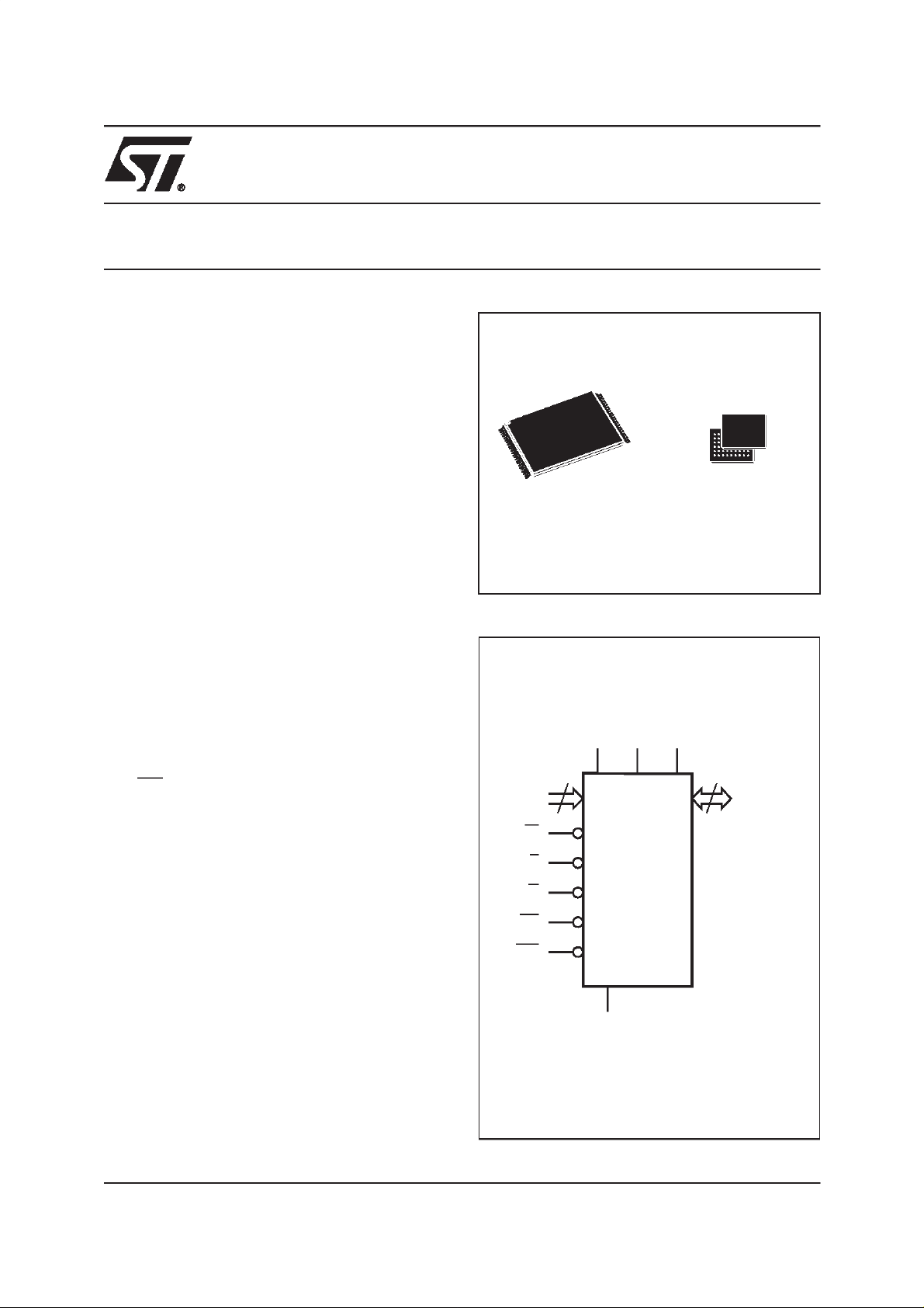
Figure 1. Logic Diagram
V
V
DD
DDQVPP
21
A0-A20
W
E
G
RP
WP
M28W320CT
M28W320CB
V
SS
PRELIMINARY DATA
µBGA
µBGA47 (GB)
8 x 6 solder balls
16
DQ0-DQ15
AI03521
May 2000
This is preliminary information on a new product now in development or undergoing evaluation. Details are subject to change without notice.
1/42
M28W320CT, M28W320CB
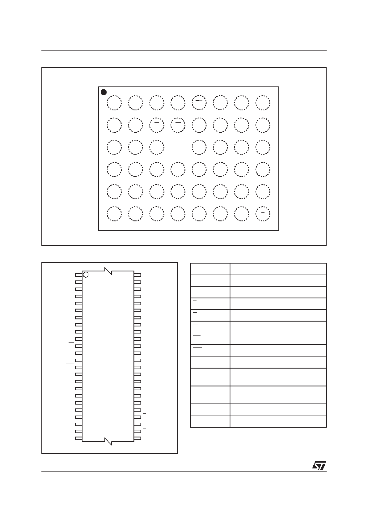
Figure 2. µBGA Connections (Top view through package)
A
A8A11A13
PP
WP
A19
87654321
A4A7V
B
C
D
E
F
DDQ
Figure 3. TSOP Connections
A15
A14
A13
A12
A11
A10 DQ14
A20
V
A19
A18
A17
1
A9
A8
NC
W
12
RP
13
PP
WP
A7
A6
A5
A4
A3
A2
24 25
A1
M28W320CT
M28W320CB
48
37
36
AI03522
RP A18
DQ7VSS
DQ13
DQ11
DQ12
DQ4
A20
DQ2
DD
DQ0DQ9DQ3DQ6DQ15V
DQ1DQ10V
A2A5A17WA10A14
A1A3A6A9A12A15
A0EDQ8DQ5DQ14A16
V
SS
G
AI02686
Table 1. Signal Names
A16
V
DDQ
V
SS
DQ15
DQ7
DQ6
DQ13
DQ5
DQ12
DQ4
V
DD
DQ11
DQ3
DQ10
DQ2
DQ9
DQ1
DQ8
DQ0
G
V
SS
E
A0
A0-A20 Address Inputs
DQ0-DQ7 Data Input/Output, Command Inputs
DQ8-DQ15 Data Input/Output
E Chip Enable
G Output Enable
W Write Enable
RP Reset
WP Write Protect
V
V
V
V
DD
DDQ
PP
SS
Supply Voltage
Power Supply for
Input/Output Buffers
Optional Supply Voltage for
Fast Program & Erase
Ground
NC Not Connected Internally
2/42

M28W320CT, M28W320CB
Table 2. Absolute Maximum Ratings
Symbol Parameter Value Unit
T
A
T
BIAS
T
STG
V
IO
V
DD,VDDQ
V
PP
Note: 1. Except for the rating ”Operating Temperature Range”, stresses above those listed in the Table ”Absolute Maximum Ratings” may
cause permanent damage to the device. These are stress ratings only and operation of the device atthese or any other conditions
above those indicated in the Operating sections of this specification is not implied. Exposure to Absolute Maximum Rating conditions for extended periodsmay affect device reliability. Referalso to the STMicroelectronics SURE Program andother relevant quality documents.
2. Depends on range.
Ambient Operating Temperature
Temperature Under Bias –40 to 125 °C
Storage Temperature –55 to 155 °C
Input or Output Voltage
Supply Voltage –0.6 to 4.1 V
Program Voltage –0.6 to 13 V
DESCRIPTION
The M28W320C is a 32 Mbit non-volatile Flash
memory thatcanbe erased electrically at theblock
level and programmed in-system on a Word-byWord basis. The device is offered in the TSOP48
(10 x 20mm) and the µBGA47, 0.75mm ball pitch
packages. When shipped, all bits of the
M28W320C are in the 1 state.
The array matrix organisation allows eachblock to
be erased and reprogrammed without affecting
other blocks. All blocks are protected against programming and erase at Power UP. Blocks can be
unprotected to make changes in the application
and then reprotected. A parameter block”Security
Block” can be permanently protected against programming and erase in order to increase the data
security. Each block can be programmed and
erased over 100,000 cycles. V
DDQ
the I/O pin down to 1.65V. An optional 12V V
power supply is provided to speed up the program
phase at customer production line environment.
An internal Command Interface (C.I.) decodes the
instructions to access/modifythe memory content.
The Program/Erase Controller (P/E.C.) automatically executes the algorithms taking care of the
timings necessary for program and erase operations. Verification is performed too, unburdening
the microcontroller, while the Status Register
tracks the status of the operation.
The following instructions are executed by the
M28W320C: Read Array, Read Electronic Signature, Read Status Register, Clear Status Register,
Program, Double Word Program, Block Erase,
Program/Erase Suspend, Program/Erase Resume, CFIQuery,Block Protect,Block Lock, Block
Unprotect, Protection Program.
Organisation
(1)
(2)
allows to drive
PP
–40 to 85 °C
–0.6 to V
DDQ
+0.6
V
Data Input/Output. Memory control is provided by
Chip Enable E, OutputEnable Gand WriteEnable
W inputs. The Program and Erase operations are
managed automatically by the P/E.C. Block protection against Program or Erase provides additional data security.
Memory Blocks
The device features an asymmetrical blocked architecture. The M28W320C has an array of 71
blocks: 8 Parameter Blocks of 4 KWord and 63
Main Blocks of 32 KWord. M28W320CT has the
Parameter Blocks at the top of the memory address space while the M28W320CB locates the
Parameter Blocks starting from the bottom. The
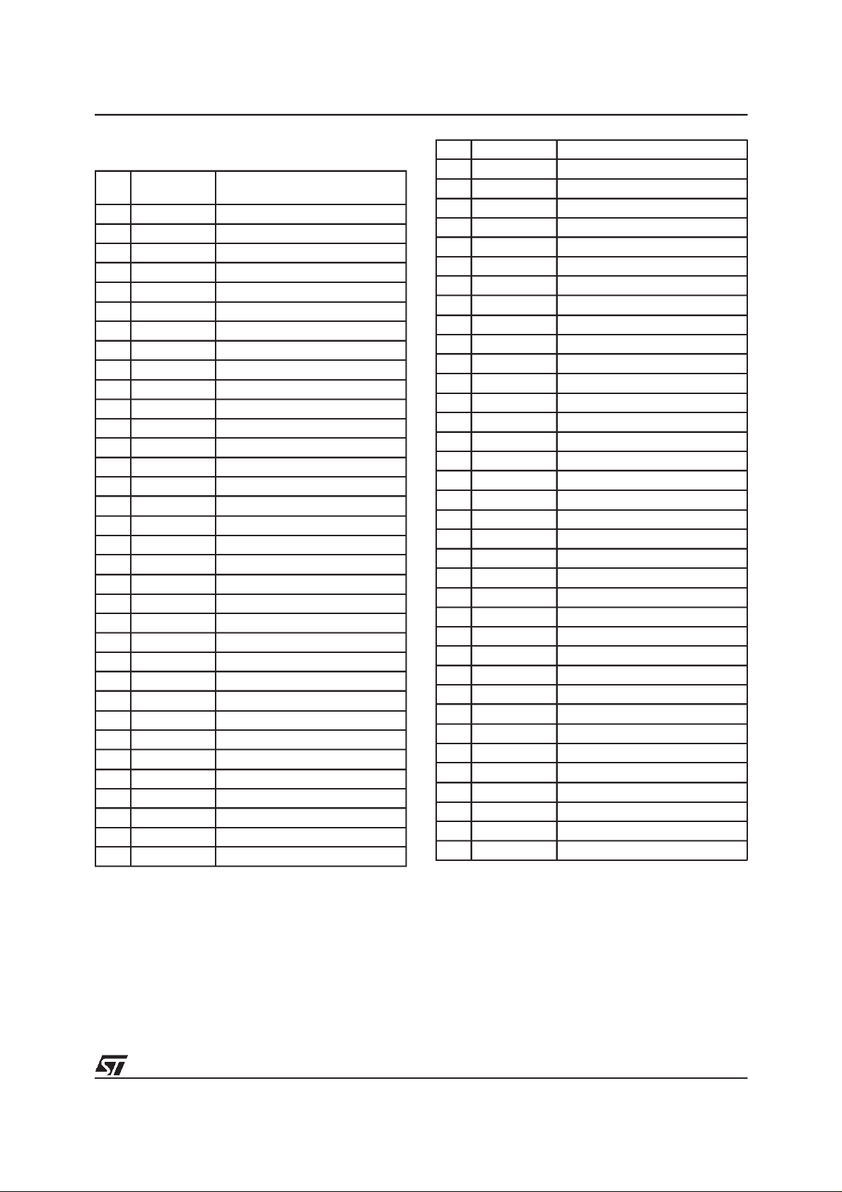
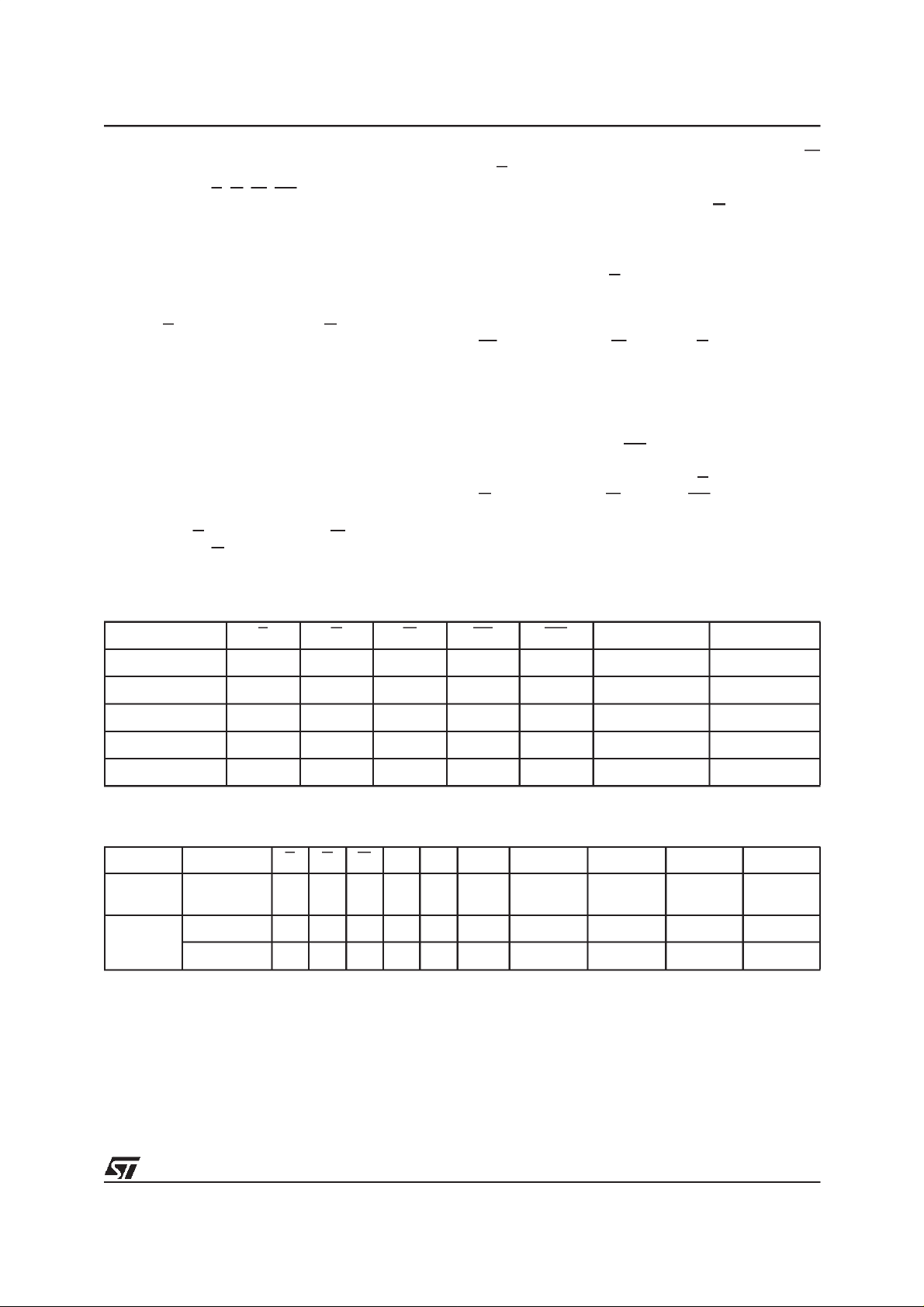
memory maps are shown in Tables 3 and 4.
All Blocks are protected at power up. Instruction
are provided to protect, unprotect any block in the
application. A second register locks the protection
status while WP is low (see Block Protection Description). Each block can be erased separately.
Erase can be suspended in order to perform either
read or program in any other block and then resumed. Program canbe suspendedto readdata in
any other block and then resumed.
The architecture includes a 128 bits Protection
register that are divided into Two 64-bits segment.
In the first one, starting from address 81h to 84h,
is written a unique device number, while the second one, starting from 85h to 88h, is programmable by the user. The user programmable segment
can be permanently protected programming the
bit.1 of the Protection Lock Register (see protection register and Security Block). The parameter
block (# 0)is asecurity block. Itcanbe permanently protected by the user programming the bit.2of
the Protection Lock Register (seeprotection register and Security Block).
The M28W320C is organised as 2 Mbit by 16 bits.
A0-A20 are the address lines; DQ0-DQ15 are the
3/42

M28W320CT, M28W320CB
Table 3. Top Boot Block Addresses,
M28W320CT
#
70 4 1FF000-1FFFFF
69 4 1FE000-1FEFFF
68 4 1FD000-1FDFFF
67 4 1FC000-1FCFFF
66 4 1FB000-1FBFFF
65 4 1FA000-1FAFFF
64 4 1F9000-1F9FFF
63 4 1F8000-1F8FFF
62 32 1F0000-1F7FFF
61 32 1E8000-1EFFFF
60 32 1E0000-1E7FFF
59 32 1D8000-1DFFFF
58 32 1D0000-1D7FFF
57 32 1C8000-1CFFFF
56 32 1C0000-1C7FFF
55 32 1B8000-1BFFFF
54 32 1B0000-1B7FFF
53 32 1A8000-1AFFFF
52 32 1A0000-1A7FFF
51 32 198000-19FFFF
50 32 190000-197FFF
49 32 188000-18FFFF
48 32 180000-187FFF
47 32 178000-17FFFF
46 32 170000-177FFF
45 32 168000-16FFFF
44 32 160000-167FFF
43 32 158000-15FFFF
42 32 150000-157FFF
41 32 148000-14FFFF
40 32 140000-147FFF
39 32 138000-13FFFF
38 32 130000-137FFF
37 32 128000-12FFFF
Size
(KWord)
Address Range
36 32 120000-127FFF
35 32 118000-11FFFF
34 32 110000-117FFF
33 32 108000-10FFFF
32 32 100000-107FFF
31 32 0F8000-0FFFFF
30 32 0F00000-F7FFF
29 32 0E8000-0EFFFF
28 32 0E0000-0E7FFF
27 32 0D8000-0DFFFF
26 32 0D0000-0D7FFF
25 32 0C8000-0CFFFF
24 32 0C0000-0C7FFF
23 32 0B8000-0BFFFF
22 32 0B0000-0B7FFF
21 32 0A8000-0AFFFF
20 32 0A0000-0A7FFF
19 32 098000-09FFFF
18 32 090000-097FFF
17 32 088000-08FFFF
16 32 080000-087FFF
15 32 078000-07FFFF
14 32 070000-077FFF
13 32 068000-06FFFF
12 32 060000-067FFF
11 32 058000-05FFFF
10 32 050000-057FFF
9 32 048000-04FFFF
8 32 040000-047FFF
7 32 038000-03FFFF
6 32 030000-037FFF
5 32 028000-02FFFF
4 32 020000-027FFF
3 32 018000-01FFFF
2 32 010000-017FFF
1 32 008000-00FFFF
0 32 000000-007FFF
4/42
M28W320CT, M28W320CB
Table 4. Bottom Boot Block Addresses,
M28W320CB
#
70 32 1F8000-1FFFFF
69 32 1F0000-1F7FFF
68 32 1E8000-1EFFFF
67 32 1E0000-1E7FFF
66 32 1D8000-1DFFFF
65 32 1D0000-1D7FFF
64 32 1C8000-1CFFFF
63 32 1C0000-1C7FFF
62 32 1B8000-1BFFFF
61 32 1B0000-1B7FFF
60 32 1A8000-1AFFFF
59 32 1A0000-1A7FFF
58 32 198000-19FFFF
57 32 190000-197FFF
56 32 188000-18FFFF
55 32 180000-187FFF
54 32 178000-17FFFF
53 32 170000-177FFF
52 32 168000-16FFFF
51 32 160000-167FFF
50 32 158000-15FFFF
49 32 150000-157FFF
48 32 148000-14FFFF
47 32 140000-147FFF
46 32 138000-13FFFF
45 32 130000-137FFF
44 32 128000-12FFFF
43 32 120000-127FFF
42 32 118000-11FFFF
41 32 110000-117FFF
40 32 108000-10FFFF
39 32 100000-107FFF
38 32 0F8000-0FFFFF
37 32 0F0000-0F7FFF
Size
(KWord)
Address Range
36 32 0E8000-0EFFFF
35 32 0E0000-0E7FFF
34 32 0D8000-0DFFFF
33 32 0D0000-0D7FFF
32 32 0C8000-0CFFFF
31 32 0C0000-0C7FFF
30 32 0B8000-0BFFFF
29 32 0B0000-0B7FFF
28 32 0A8000-0AFFFF
27 32 0A0000-0A7FFF
26 32 098000-09FFFF
25 32 090000-097FFF
24 32 088000-08FFFF
23 32 080000-087FFF
22 32 078000-07FFFF
21 32 070000-077FFF
20 32 068000-06FFFF
19 32 060000-067FFF
18 32 058000-05FFFF
17 32 050000-057FFF
16 32 048000-04FFFF
15 32 040000-047FFF
14 32 038000-03FFFF
13 32 030000-037FFF
12 32 028000-02FFFF
11 32 020000-027FFF
10 32 018000-01FFFF
9 32 010000-017FFF
8 32 008000-00FFFF
7 4 007000-007FFF
6 4 006000-006FFF
5 4 005000-005FFF
4 4 004000-004FFF
3 4 003000-003FFF
2 4 002000-002FFF
1 4 001000-001FFF
0 4 000000-000FFF
5/42

M28W320CT, M28W320CB
SIGNAL DESCRIPTIONS
See Figure 1 and Table 1.
Address Inputs (A0-A20). The address signals
are inputs driven with CMOS voltage levels. They
are latched during a write operation.
Data Input/Output (DQ0-DQ15). The data in-
puts, a word to be programmed or a command to
the C.I., are latched on the Chip Enable E or Write
Enable W rising edge, whichever occurs first. The
data output from the memoryArray, theElectronic
Signature, the block protection status or Status
Register is valid when Chip Enable E and Output
Enable Gareactive. Theoutput is high impedance
when the chip is deselected, the outputs are disabled or RP is tied to VIL. Commands are issued
on DQ0-DQ7.
Chip Enable (E). The Chip Enable input activates the memory control logic, input buffers, decoders and sense amplifiers. E at VIHdeselects
the memory and reduces the power consumption
to thestand-by level. E can also beused to control
writing to the command register andto the memory array, while W remains at VIL.
Output Enable (G). The Output Enable controls
the data Input/Output buffers.
Write Enable (W). This input controls writing to
the Command Register, Input Address and Data
latches.
Write Protect (WP). This input gives an additional hardware protection level against program or
erase whenpulled atVIL, asdescribed in theBlock
Protection description.
Reset Input (RP). The RP input provides hardware reset of the memory. When RP is at VIL,the
memory is in reset mode: the outputs are put to
High-Z and the current consumption is minimised.
When RP is at VIH, the device is in normal operation. Exiting reset mode thedevice entersread array mode.
VDDSupply Voltage (2.7V to 3.6V). V
DD
provides the power supply to the internal core of the
memory device. It is the main power supply for all
operations (Read, Program and Erase). It ranges
from 2.7V to 3.6V.
V
Supply Voltage (1.65V to VDD). V
DDQ
DDQ
provides the power supply to the I/O pins and enables all Outputs to be powered independently
from VDD.V
can be tied to VDDor it can use a
DDQ
separate supply. It can be powered either from
1.65V to VDD.
VPPProgram Supply Voltage (12V). VPPis both
a control input and a power supply pin. The two
functions are selected by the voltage range applied to the pin.
If VPPis kept in a low voltage range (0V to 3.6V)
VPPis seen as a control input. In this case a voltage lowerthan V
against program or erase, while VPP>V
gives an absolute protection
PPLK
PP1
enables these functions. VPPvalue is only sampled
at the beginning of a program or erase; a change
in its value after the operation has been started
does not haveany effectandprogram or erase are
carried on regularly.
If VPPis used in the range 11.4V to 12.6V acts as
a power supply pin. In this condition VPPvalue
must be stable until P/E algorithm is completed
(see Table 24 and 25).
VSSGround. VSSis the reference for all the volt-
age measurements.
6/42
M28W320CT, M28W320CB
DEVICE OPERATIONS
Four control pins rule the hardware access to the
Flash memory: E, G, W, RP. The following operations can be performed using the appropriate bus
cycles: Read, Write the Command of an Instruction, Output Disable, Stand-by, Reset (see Table
5).
Read. Read operations are used to output the
contents of the Memory Array, the Electronic Signature, the Status Registerand the CFI. Both Chip
Enable (E) and Output Enable (G) must be at V
in order to perform the read operation. The Chip
Enable input should beused to enable the device.
Output Enable should be used to gate data onto
the output independently of the device selection.
The data read depend on the previous command
written to the memory (see instructions RD,RSIG,
RSR, RCFI). Read Array is the default state of the
device when exiting reset or after power-up.
Write. Write operations are used to give Commands to the memory or to latch Input Data to be
programmed. A write operation is initiated when
Chip Enable E and Write Enable W are at VILwith
Output Enable G at VIH. Commands, Input Data
Table 5. User Bus Operations
Operation E G W RP WP
Read
Write
Output Disable V
Stand-by
Reset X X X
Note: 1. X = VILor VIH,V
V
IL
V
IL
IL
V
IH
= 12V ± 5%.
PPH
(1)
V
IL
V
IH
V
IH
XX
V
IH
V
IL
V
IH
andAddresses arelatched on the rising edgeof W
or E, whichever occur first.
Output Disable. The data outputs are high impedance when the Output Enable G is at VIH.
Stand-by. Stand-by disables most of the internal
circuitry allowing a substantial reductionofthe current consumption. The memory is in stand-by
when Chip Enable E is at VIHand the device is in
read mode. The power consumption is reduced to
the stand-by level and the outputs are set to high
impedance, independently fromthe Output Enable
IL
G or Write Enable W inputs. If E switches to V
during program or erase operation, the device enters in stand-by when finished.
Reset. During Reset mode all internal circuits are
switched off, the memory is deselected and the
outputs are put in high impedance. The memory is
in Reset mode when RP is at VIL. The power consumption is reduced to the stand-by level, independently from the Chip Enable E, Out-put Enable
G or Write Enable W inputs. If RP is pulled to V
during aProgram or Erase, this operation is aborted and the memory content is no longer valid as it
has been compromised by the aborted operation.
V
IH
V
IH
V
IH
V
IH
V
IL
V
PP
X Don’t Care Data Output
V
X
X Don’t Care Hi-Z
X Don’t Care Hi-Z
X Don’t Care Hi-Z
DD
or V
PPH
DQ0-DQ15
Data Input
IH
SS
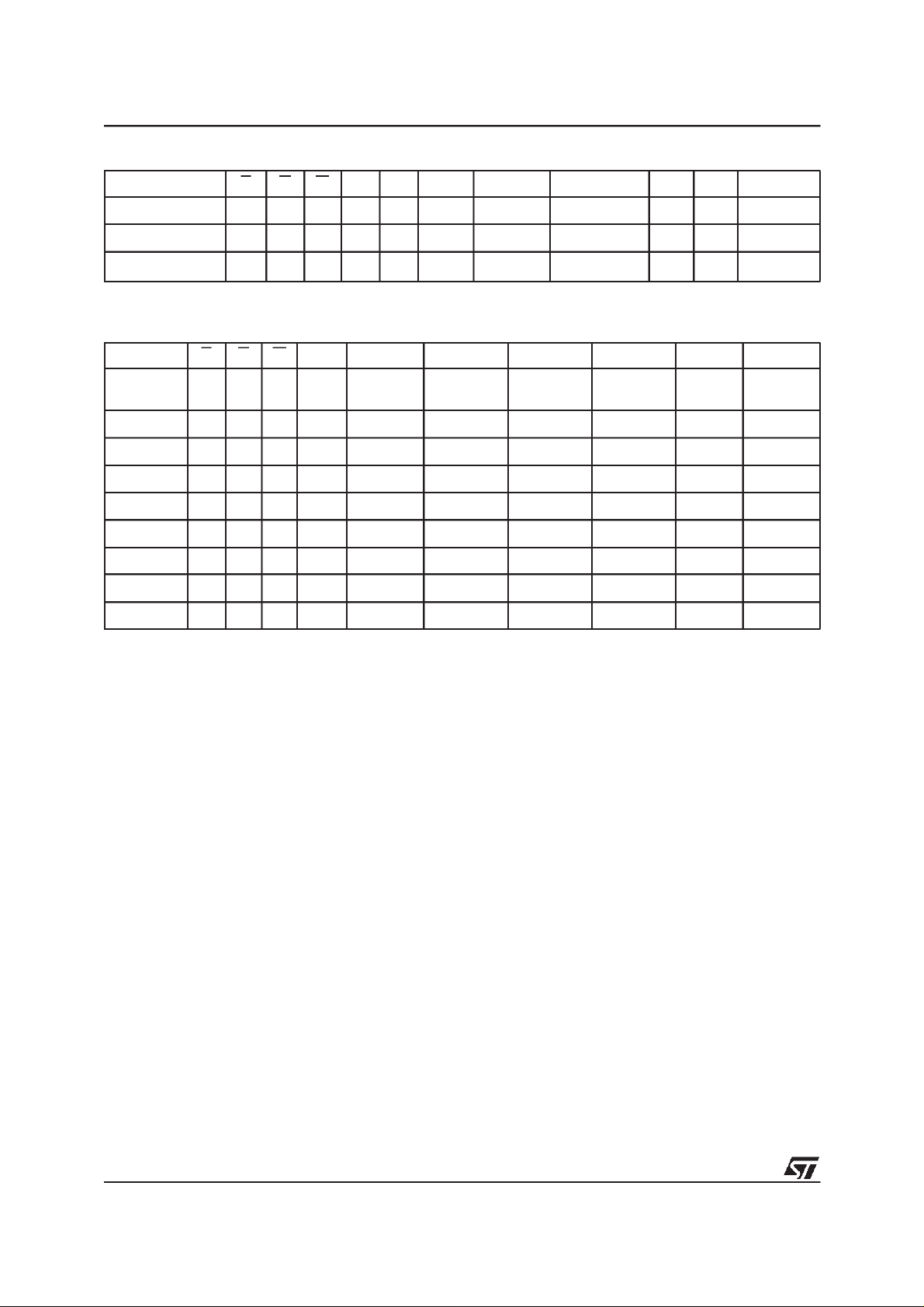
Table 6. Read Electronic Signature (RSIG Instruction)
Code Device E G W A0 A1 A2-A7 A8-A11 A12-A20 DQ0-DQ7 DQ8-DQ15
Manufact.
Code
Device
Code
M28W320CT
M28W320CB
V
ILVILVIHVILVIL
V
ILVILVIHVIHVIL
V
ILVILVIHVIHVIL
0 Don’t Care Don’t Care 20h 00h
0 Don’t Care Don’t Care BAh 88h
0 Don’t Care Don’t Care BBh 88h
7/42
M28W320CT, M28W320CB
Table 7. Read Block Signature (RSIG Instruction)
Block Status E G W A0 A1 A2-A7 A8-A11 A12-A20 DQ0 DQ1 DQ2-DQ15
Protected Block
Unprotected Block V
Locked Block
Note: 1. A Locked Block can be protected ”DQ0 = 1” or unprotected ”DQ0 = 0”; see Block protection section.
Table 8. Read Protection Register and Protection Register Lock (RSIG Instruction)
Word E G W A0-A7 A8-A20 DQ0 DQ1 DQ2 DQ3-DQ7 DQ8-DQ15
Lock
Unique Id 0
Unique Id 1 V
Unique Id 2
Unique Id 3
OTP 0
OTP 1
OTP 2
OTP 3
V
ILVILVIHVILVIH
ILVILVIHVILVIH
V
ILVILVIHVILVIH
V
ILVILVIH
V
ILVILVIH
ILVILVIH
V
ILVILVIH
V
ILVILVIH
V
ILVILVIH
V
ILVILVIH
V
ILVILVIH
V
ILVILVIH
0 Don’t Care Block Address 1 0 00h
0 Don’t Care Block Address 0 0 00h
0 Don’t Care Block Address
80h Don’t Care 0
OTP Prot.
data
Security
prot. data
(1)
X
00h 00h
1
81h Don’t Care ID data ID data ID data ID data ID data
82h Don’t Care ID data ID data ID data ID data ID data
83h Don’t Care ID data ID data ID data ID data ID data
84h Don’t Care ID data ID data ID data ID data ID data
85h Don’t Care OTP data OTP data OTP data OTP data OTP data
86h Don’t Care OTP data OTP data OTP data OTP data OTP data
87h Don’t Care OTP data OTP data OTP data OTP data OTP data
88h Don’t Care OTP data OTP data OTP data OTP data OTP data
00h
8/42

M28W320CT, M28W320CB
INSTRUCTIONS AND COMMANDS
Sixteen instructions are available (see Tables 9
and 10)to perform Read MemoryArray, Read Status Register, Read Electronic Signature, CFI Query, Erase, Program, Double Word Program, Clear
Status Register, Program/Erase Suspend, Program/Erase Resume, Block Protect, Block Unprotect, Block Lockand Protection Register Program.
Status Register output may be read at any time,
during programming or erase, to monitor the
progress of the operation.
An internal Command Interface (C.I.) decodes the
instructions while an internal Program/Erase Controller (P/E.C.) handles all timing and verifies the
correct execution of the Program and Erase instructions. P/E.C. provides a Status Register
whose bitsindicate operationand exit status ofthe
internal algorithms.
The Command Interface is reset to Read Array
when power is first applied, when exiting from Reset or whenever VDDis lower than V
LKO
. Command sequence must be followed exactly. Any
invalid combinationof commandswill reset thedevice to Read Array.
Read (RD)
The Read instruction consists of one write cycle
(refer to Device Operations section) giving the
command FFh. Next read operations will read the
addressed location and output the data. When a
device reset occurs, the memory is in Read Array
as default.
Read Status Register (RSR)
The Status Register indicates when a program or
erase operation is complete and the success or
failure of operation itself. Issue a Read Status
Register Instruction (70h) to read the Status Register content.TheRead StatusRegister instruction
may be issued at any time, also when a Program/
Erase operation is ongoing. The following Read
operations output the content of the Status Register. The Status Register is latched on the falling
edge of E or G signals, and can be read until E or
G returns to VIH. Either E or G must be toggled to
update the latched data. Additionally, any read attempt during programor erase operation will automatically outputthe content of the Status Register.
Read Electronic Signature (RSIG)
The Read Electronic Signature instruction consists of onewrite cycle (refer toDevice Operations
section) giving the command 90h. A subsequent
read will output the Manufacturer Code, the Device Code,the Block protection Status, orthe Protection Register. See Tables 6, 7 and 8 for the
valid address. The Electronic Signature can be
read from the memory allowing programming
equipment or applications to automatically match
their interface to the characteristics of
M28W320C.
CFI Query (RCFI)
The Common Flash Interface Query mode is enteredby writing98h. Next readoperations will read
the CFI data. The CFI data structure contains also
a security area; in this section, a 64 bit unique security number is written, starting at this address
81h. Thisarea can be accessed only in read mode
and there are no ways of changing the code after
it has been written by ST. Write a read instruction
to return to Read mode (refer to the Common
Flash Interface section).
Table 9. Commands
Hex Code Command
00h Invalid/Reserved
10h Alternative Program Set-up
20h Erase Set-up
30h Double Word Program Set-up
40h Program Set-up
50h Clear Status Register
70h Read Status Register
90h or 98h
B0h Program/Erase Suspend
D0h
FFh Read Array
01h Protect Confirm
2Fh Lock Confirm
C0h Protection Program
60h Protection Set-up
Read Electronic Signature, or
CFI Query
Program/Erase Resume, Erase
Confirm or Unprotect Confirm
9/42

M28W320CT, M28W320CB
Table 10. Instructions
Mne-
monic
RD
RSR
RSIG
RCFI Read CFI 1+ Write 55h
EE Erase 2 Write X 20h Write
PG Program 2 Write X
DPG
CLRS
PES
PER
BP Block Protect 2 Write X 60h Write
BU
BL Block Lock 2 Write X 60h Write
PRP
Note: 1. X = Don’t Care.
Instruction Cycles
Read Memory
Array
Read Status
Register
Read
Electronic
Signature
Double Word
(4)
Program
Clear Status
(5)
Register
Program/
Erase
Suspend
Program/
Erase
Resume
Block
Unprotect
Protection
Register
Program
2. The first cycle of the RD, RSR, RSIG or RCFI instruction is followed byread operations in the memory arrayor special register. Any
number of read cycle can occur after one command cycle.
3. The signature address recognized are listed in the Tables 6, 7 and 8.
4. Address 1 and Address 2 must be consecutive address differing only for address bit A0.
5. A read cycle after a CLSR instruction willoutput the memory array.
Operat.
1+ Write X FFh
1+ Write X 70h
1+ Write X
3 Write X 30h Write Address 1
1 Write X 50h
1 Write X B0h
1 Write X D0h
2 Write X 60h Write
2 Write X C0h Write Address
1st Cycle 2nd Cycle 3nd Cycle
(1)
Addr.
Data Operat. Addr. Data Operat. Addr. Data
Read
90h or
98h
98h or
90h
40h or
10h
(2)
Read
Read
Read
Read
Write Address
(2)
(2)
(2)
Address
Signature
Address
CFI
Address
Block
Address
Block
Address
Block
Address
Block
Address
X
(3)
Data
Status
Register
Data
Query
D0h
Data
Input
Data
Input
01h
D0h
2Fh
Data
Input
Write Address 2
Data
Input
Erase (EE)
Block erasure sets all the bits within the selected
block to ’1’. One block at a time can be erased. It
is not necessary to program the block with 00h as
the P/E.C. will do it automatically before erasing.
This instruction uses two write cycles. The first
command written is the Erase Set up command
20h. The second command is the Erase Confirm
command D0h. An address within the block to be
erased is given and latched into the memory during the input of the second command. If the second command given is not an erase confirm, the
status register bits b4 and b5 are set and the instruction aborts.
Read operations output the status register after
erasure has started.
10/42
Status Register bitb7 returns ’0’ while the erasure
is in progress and’1’when it has completed. After
completion the Status Register bit b5 returns ’1’ if
there has been an Erase Failure. Status register
bit b1 returns ’1’ if the user is attempting to program a protected block. Status Register bit b3 returns a ’1’ if VPPis below V
PPLK
.
Erase aborts if RP turns to VIL. As data integrity
cannot beguaranteed whenthe erase operation is
aborted, the erase mustbe repeated. A ClearStatus Register instructionmust beissued toreset b1,
b3, b4 and b5 of the Status Register. During the
execution of the erase by the P/E.C., the memory
accepts only the RSR (Read Status Register) and
PES (Program/Erase Suspend) instructions.
M28W320CT, M28W320CB
(2)
(1)
Next State After Event
(3)
Protect Unprotect Lock WP transition
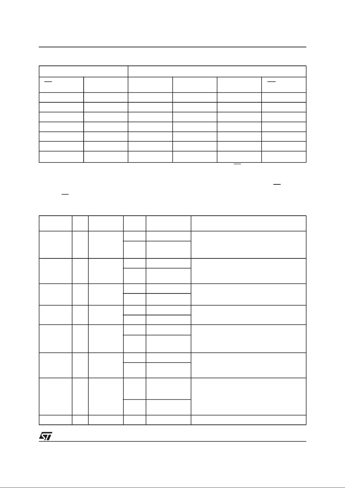
Table 11. Protection States
Current State
(WP,DQ1, DQ0)
Program/Erase
Allowed
100 yes 101 100 111 000
101 no 101 100 111 001
110 yes 111 110 111 011
111 no 111 110 111 011
000 yes 001 000 011 100
001 no 001 000 011 101
011 no 011 011 011
Note: 1. All blocks are protected at power-up, so the default configuration is 001 or 101 according to WP status.
2. Current state and Next state gives the protection status of a block. The protection status is defined by the write protect pin and by
DQ1 (=1 for a locked block) and DQ0 (= 1 for a protected block) as read in the Read Electronic Signature instruction with A1 = V
and A0 = VIL.
3. Next state isthe protection statusof ablock after aProtect orUnprotect orLock command hasbeen issued or after WP haschanged
its logic value.
4. A WP transition to V
ona locked block will restore the previous DQ0 value, giving a 111 or 110.
IH
111 or 110
Table 12. Status Register Bits
Mnemonic Bit Name
P/ECS 7 P/E.C. Status
Erase
ESS 6
Suspend
Status
ES 5 Erase Status
PS 4
VPPS 3
Program
Status
Status
V
PP
Program
PSS 2
Suspend
Status
Block
BPS 1
Protection
Status
0 Reserved
Note: Logic level ’1’is High, ’0’ is Low.
Logic
Level
Definition Note
’1’ Ready Indicates the P/E.C. status, check during
Program or Erase, and on completion before
’0’ Busy
’1’ Suspended
In progress or
’0’
Completed
checking bits b4 or b5 for Program or Erase
Success.
On an Erase Suspend instruction P/ECS and
ESS bits are set to’1’.ESS bit remains ’1’until an
Erase Resume instruction is given.
’1’ Erase Error ES bit is set to ’1’ if P/E.C. has applied the
maximum number of erase pulses to the block
’0’ Erase Success
’1’ Program Error
’0’ Program Success
Invalid, Abort V
V
’1’
PP
without achieving an erase verify.
PS bit set to ’1’ if the P/E.C. has failed to program
a word.
bit is set if the VPPvoltage is below V
PPS
when aProgram or Erase instruction is executed.
V
is sampled only at the beginning of the
’0’
PP
OK
V
’1’ Suspended
In Progress or
’0’
Completed
PP
erase/program operation.
On a Program Suspend instruction P/ECS and
PSS bits are set to ’1’. PSS remains ’1’ until a
Program Resume Instruction is given.
Program/Erase on
’1’
protected Block,
Abort
No operation to
’0’
protected blocks
BPS bit is set to ’1’ if a Program or Erase
operation has been attempted on a protected
block.
(4)
IH
PPLK
11/42

M28W320CT, M28W320CB
Program (PG)
The memory array can be programmed word-byword. This instruction uses two write cycles. The
first command written is the Program Set-up command 40h(or 10h).A second write operation latches the Address and the Data to be written and
starts the P/E.C.
Read operations output the Status Register content afterthe programming hasstarted. TheStatus
Register bit b7 returns ’0’ while the programming
is in progress and ’1’ when it has completed. After
completion the Status register bit b4 returns ’1’ if
there has been a Program Failure. Status register
bit b1 returns ’1’ if the user is attempting to program a protected block. StatusRegister bit b3 returns a ’1’ if VPPis below V
. Programming
PPLK
aborts if RP goes to VIL. As data integrity cannot
be guaranteed when the program operation is
aborted, the memory location must be erased and
reprogrammed. A Clear Status Register instruction must be issued to reset b4, b3 and b1 of the
Status Register.
During the execution ofthe programby theP/E.C.,
the memory accepts only the RSR (Read Status
Register) and PES (Program/Erase Suspend) instructions.
Double Word Program (DPG)
This featureis offered to improve theprogramming
throughput, writing a page of two adjacent words
in parallel.The two words must differ only for the
address A0. Programming should not be attempted when VPPis not at V
also be executed if VPPis below V
. The operation can
PPH
PPH
but result
could be uncertain. This instruction uses three
write cycles.The first commandwritten isthe Double Word Program Set-Up command 30h. A second write operation latches the Address and the
Data of the first word to be written, the third write
operation latches the Address and the Data of the
second word to be written and starts the P/E.C.
Read operations output the Status Register content afterthe programming hasstarted. TheStatus
Register bit b7 returns ’0’ while the programming
is in progress and ’1’ when it has completed. After
completion the Status register bit b4 returns ’1’ if
there has been a Program Failure. Status register
bit b1 returns ’1’ if the user is attempting to program a protected block. StatusRegister bit b3 returns a ’1’ if VPPis below V
. Programming
PPLK
aborts if RP goes to VIL. As data integrity cannot
be guaranteed when the program operation is
aborted, the memory location must be erased and
reprogrammed. A Clear Status Register instruc-
tion must be issued to reset b4, b3 and b1 of the
Status Register.
During the execution of the program by theP/E.C.,
the memory accepts only the RSR (Read Status
Register) and PES (Program/Erase Suspend) instructions.
Clear Status Register (CLRS)
The Clear Status Register uses a single write operation which clears bits b1, b3,b4 and b5to 0. Its
use is necessary before any new operation when
an error has been detected.
The Clear Status Register is executed writing the
command 50h.
Program/Erase Suspend (PES)
Program/Erase suspend is accepted only during
the Program Erase instruction execution. When a
Program/Erase Suspend command is written to
the C.I., the P/E.C. freezes the Program/Erase operation. Program/Erase Resume (PER) continues
the Program/Erase operation. Program/Erase
Suspend consists of writing the command B0h
without any specific address.
The Status Register bit b2 is set to ’1’ (within 5µs)
when the program has been suspended. b2 is set
to ’0’ in case the program is completed or in
progress. The Status Register bit b6 is set to ’1’
(within 30µs) when the erase has been suspended. b6 is set to ’0’ in case the erase is completed
or inprogress. The valid commands while erase is
suspended are: Program/Erase Resume, Program, Read Array, Read Status Register, Read
Identifier, CFI Query, Block Protect, Block Unprotect, Block Lockand Protection Program.The user
can protect the Block being erased issuing the
Block Protect, Block Lock or Protection Program
commands. In this case the protection status bit
will change immediately, but when theerase is resumed, theoperation will completeThe valid commands whileprogram is suspended are: Program/
Erase Resume, Read Array, Read Status Register, Read Identifier, CFI Query.
During program/erase suspend mode, the chip
can be placed in a pseudo-stand-by mode by taking E to VIHThis reduces active currentconsumption. Program/Erase is aborted if RP turns to VIL.
Program/Erase Resume (PER)
If a Program/Erase Suspend instruction was previously executed, the program/erase operation may
be resumed by issuing the command D0h. The
status register bit b2/b6 is cleared when program/
erase resumes. Read operations outputthe status
register after the program/erase is resumed.
12/42

M28W320CT, M28W320CB
The suggested flow charts for programs that use
the programming, erasure and program/erase
suspend/resume features of the memories are
shown from Figures 11, 12, 13, 14 and 15.
Protection Register Program (PRP)
The Protection Register Program uses two write
cycles. The first command written is the protection
program command C0h. The second write operation latchesthe Addressand the Datato bewritten
to the Protection Register(see Protection Register
and Security Block) and start the PE/C. Read operations output the Status Register content after
the programming has started. The 64 bits user
programmable Segment (85h to 88h) are programmed 16 bits at a time, it can be protected by
the user programming bit 1 of the Protection Lock
register. The bit 1 of the Protection Lock register
protect the bit 2 of the Protection Lock Register.
Writing thebit 2 of theProtection Lock Registerwill
result in a permanent protection of the Security
Block. Attemptingto program apreviously protected protection Register will result in a status register error(bit 1and bit 4of the statusregister will be
set to’1’).The protectionof the Protection Register
and/or the Security Block is not reversible.
The Protection Register Program cannot be suspended.
Block Protect (BP)
The BP instruction use two write cycles. The first
command written is the protection setup 60h. The
second command is block Protect command 01h.
The address within theblock being protected must
be given in orderto write theprotection state.If the
second command is not recognized by the C.I the
bit 4 and bit 5 of thestatus register willbe set to indicate a wrong sequence of commands. To read
the status register write the RSR command.
Block Unprotect (BU)
The instruction use two write cycles. The firstcommand written is the protection setup 60h. Thesecond command is block Unprotect command d0h.
The address within the block being unprotected
must be given in order to write the unprotection
state. If the second commandis notrecognized by
the C.I the bit 4 and bit5 of the status register will
be set to indicate a wrong sequence of commands. To read the status register write the RSR
command.
Block Lock (BL)
The instruction use two write cycles. The firstcommand written is the protection setup 60h. Thesecond command is block Lock command 2Fh. The
address within the block being Locked must be
given in order to write the Lockingstate. If the secondcommand is not recognized by the C.Ithebit 4
andbit 5of the status register will be set to indicate
a wrong sequence of commands. To read the status register write the RSR command.
Table 13. Program, Erase Times and Program/Erase Endurance Cycles
(TA= 0 to 70°C or –40 to 85°C; VDD= 2.7V to 3.6V)
Parameter Test Conditions
Word Program
Double Word Program
Main Block Program
Parameter Block Program
Main Block Erase
Parameter Block Erase
Program/Erase Cycles (per Block) 100,000 cycles
Note: TA=25°C.
V
PP=VDD
V
= 12V ±5%
PP
V
= 12V ±5%
PP
V
PP=VDD
V
= 12V ±5% 0.02 4 sec
PP
V
PP=VDD
V
= 12V ±5% 1 10 sec
PP
V
PP=VDD
= 12V ±5%
V
PP
V
PP=VDD
Min
M28W320C
(1)
Typ
10 200 µs
10 200 µs
0.16 5 sec
0.32 5 sec
0.04 4 sec
110 sec
0.8 10 sec
0.8 10 sec
Max
Unit
13/42
 Loading...