

32 Mbit (2Mb x16, Boot Block) Low Voltage Flash Memory
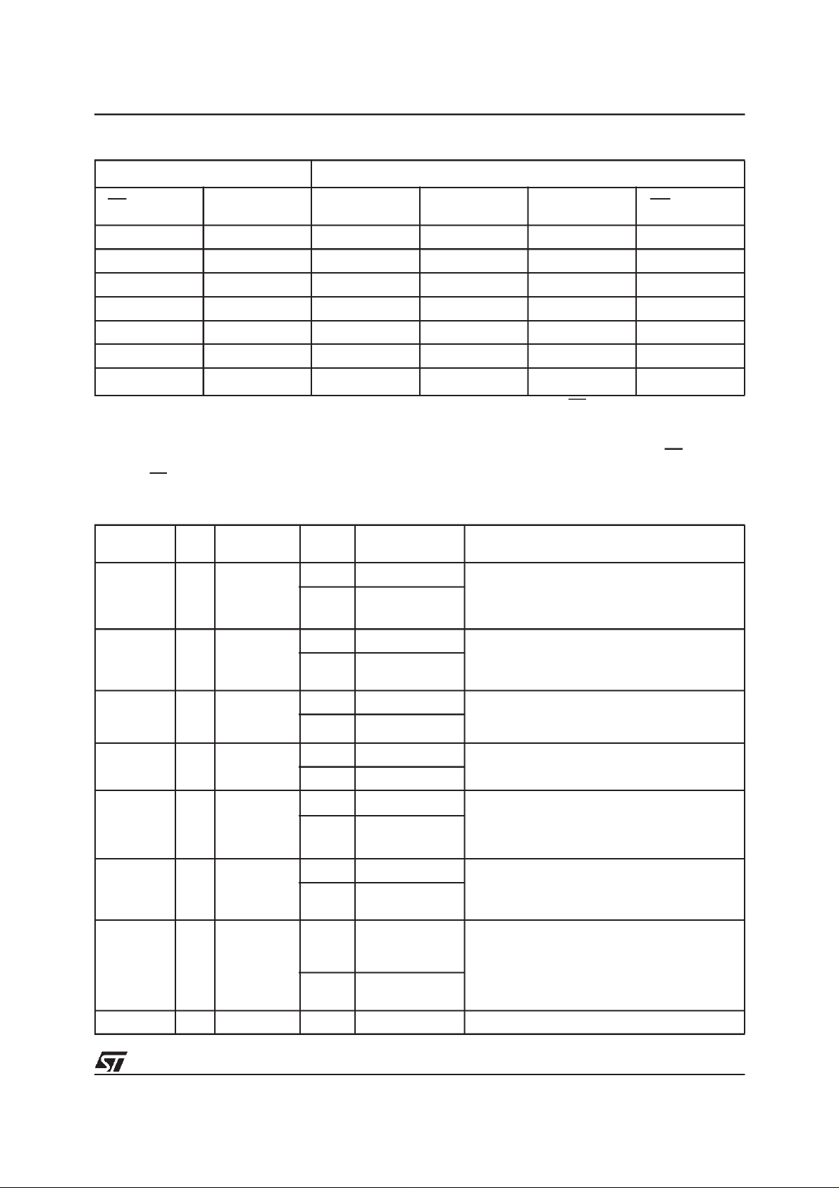
■ SUPPLY VOLTAGE
–VDD= 2.7V to 3.6V: for Program, Erase and
Read
–V
–VPP= 12V: optional Supply Voltage for fast
■ ACCESS TIME
– 2.7V to 3.6V: 90ns
– 2.7V to 3.6V: 100ns
■ PROGRAMMING TIME:
–10µs typical
– Double Word Programming Option
■ PROGRAM/ERASE CONTROLLER (P/E.C.)
■ COMMON FLASH INTERFACE
■ MEMORY BLOCKS
– Parameter Blocks (Top or Bottom location)
– MainBlocks
■ BLOCK PROTECTION UNPROTECTION
– All Blocks protected at Power Up
– Any combination of blocks can be protected
– WPfor block locking
■ SECURITY
– 64-bit user Programmable OTP cells
– 64-bit unique device identifier
– One Parameter Block Permanently Lockable
■ AUTOMATICSTAND-BY MODE
■ PROGRAM andERASE SUSPEND
■ 100,000 PROGRAM/ERASE CYCLES per
BLOCK
■ 20 YEARS of DATA RETENTION
– Defectivity below 1ppm/year
■ ELECTRONIC SIGNATURE
– Manufacturer Code: 20h
– Top Device Code, M28W320CT: 88BAh
– Bottom Device Code, M28W320CB: 88BBh
= 1.65V or 2.7V: Input/Output option
DDQ
Program
M28W320CT
M28W320CB
TSOP48 (N)
12 x 20mm
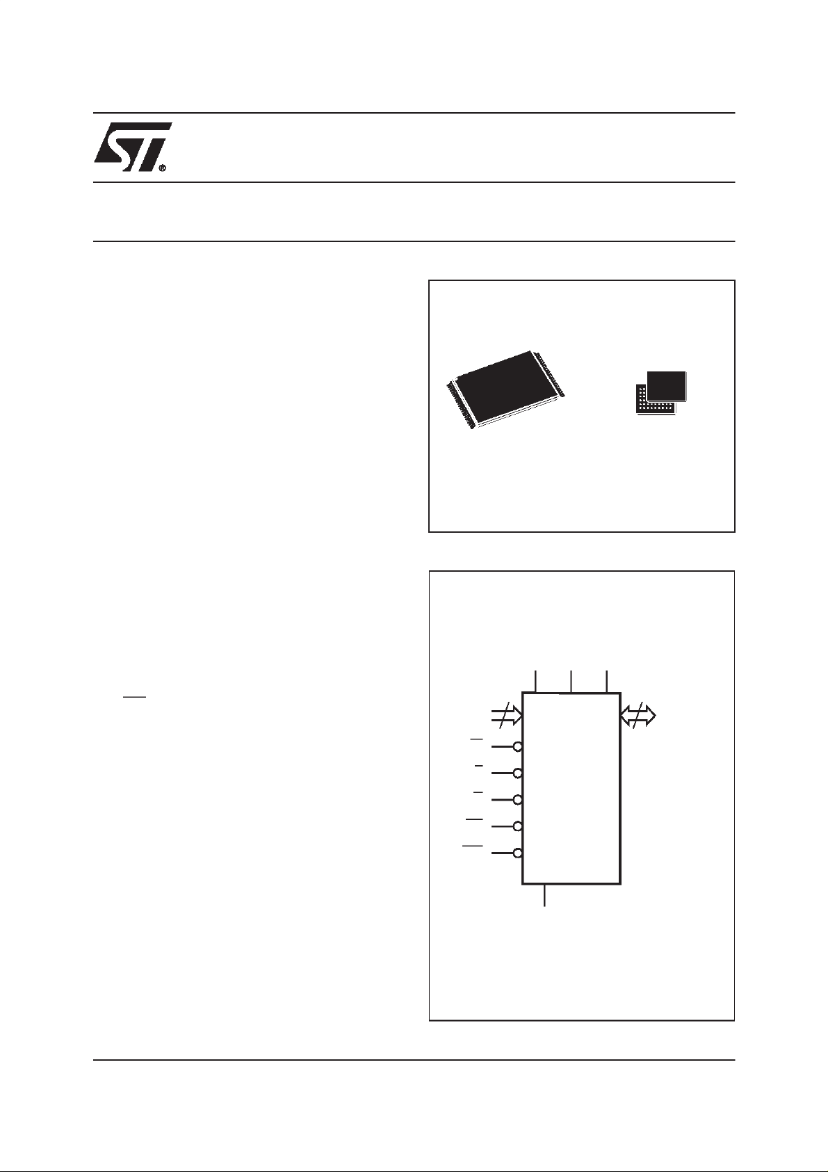
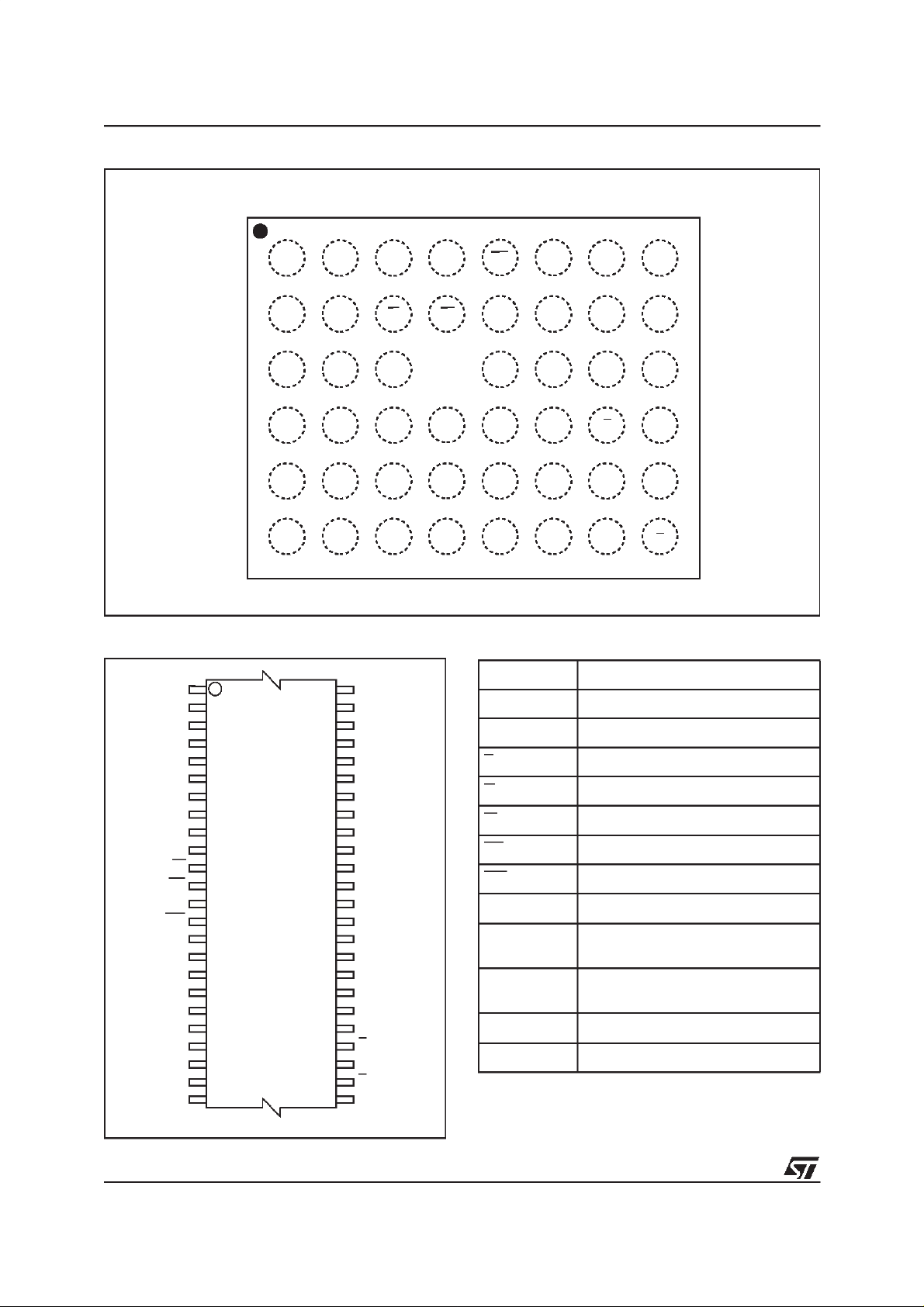
Figure 1. Logic Diagram
V
V
DD
DDQVPP
21
A0-A20
W
E
G
RP
WP
M28W320CT
M28W320CB
V
SS
PRELIMINARY DATA
µBGA
µBGA47 (GB)
8 x 6 solder balls
16
DQ0-DQ15
AI03521
May 2000
This is preliminary information on a new product now in development or undergoing evaluation. Details are subject to change without notice.
1/42
M28W320CT, M28W320CB
Figure 2. µBGA Connections (Top view through package)
A
A8A11A13
PP
WP
A19
87654321
A4A7V
B
C
D
E
F
DDQ
Figure 3. TSOP Connections
A15
A14
A13
A12
A11
A10 DQ14
A20
V
A19
A18
A17
1
A9
A8
NC
W
12
RP
13
PP
WP
A7
A6
A5
A4
A3
A2
24 25
A1
M28W320CT
M28W320CB
48
37
36
AI03522
RP A18
DQ7VSS
DQ13
DQ11
DQ12
DQ4
A20
DQ2
DD
DQ0DQ9DQ3DQ6DQ15V
DQ1DQ10V
A2A5A17WA10A14
A1A3A6A9A12A15
A0EDQ8DQ5DQ14A16
V
SS
G
AI02686
Table 1. Signal Names
A16
V
DDQ
V
SS
DQ15
DQ7
DQ6
DQ13
DQ5
DQ12
DQ4
V
DD
DQ11
DQ3
DQ10
DQ2
DQ9
DQ1
DQ8
DQ0
G
V
SS
E
A0
A0-A20 Address Inputs
DQ0-DQ7 Data Input/Output, Command Inputs
DQ8-DQ15 Data Input/Output
E Chip Enable
G Output Enable
W Write Enable
RP Reset
WP Write Protect
V
V
V
V
DD
DDQ
PP
SS
Supply Voltage
Power Supply for
Input/Output Buffers
Optional Supply Voltage for
Fast Program & Erase
Ground
NC Not Connected Internally
2/42

M28W320CT, M28W320CB
Table 2. Absolute Maximum Ratings
Symbol Parameter Value Unit
T
A
T
BIAS
T
STG
V
IO
V
DD,VDDQ
V
PP
Note: 1. Except for the rating ”Operating Temperature Range”, stresses above those listed in the Table ”Absolute Maximum Ratings” may
cause permanent damage to the device. These are stress ratings only and operation of the device atthese or any other conditions
above those indicated in the Operating sections of this specification is not implied. Exposure to Absolute Maximum Rating conditions for extended periodsmay affect device reliability. Referalso to the STMicroelectronics SURE Program andother relevant quality documents.
2. Depends on range.
Ambient Operating Temperature
Temperature Under Bias –40 to 125 °C
Storage Temperature –55 to 155 °C
Input or Output Voltage
Supply Voltage –0.6 to 4.1 V
Program Voltage –0.6 to 13 V
DESCRIPTION
The M28W320C is a 32 Mbit non-volatile Flash
memory thatcanbe erased electrically at theblock
level and programmed in-system on a Word-byWord basis. The device is offered in the TSOP48
(10 x 20mm) and the µBGA47, 0.75mm ball pitch
packages. When shipped, all bits of the
M28W320C are in the 1 state.
The array matrix organisation allows eachblock to
be erased and reprogrammed without affecting
other blocks. All blocks are protected against programming and erase at Power UP. Blocks can be
unprotected to make changes in the application
and then reprotected. A parameter block”Security
Block” can be permanently protected against programming and erase in order to increase the data
security. Each block can be programmed and
erased over 100,000 cycles. V
DDQ
the I/O pin down to 1.65V. An optional 12V V
power supply is provided to speed up the program
phase at customer production line environment.
An internal Command Interface (C.I.) decodes the
instructions to access/modifythe memory content.
The Program/Erase Controller (P/E.C.) automatically executes the algorithms taking care of the
timings necessary for program and erase operations. Verification is performed too, unburdening
the microcontroller, while the Status Register
tracks the status of the operation.
The following instructions are executed by the
M28W320C: Read Array, Read Electronic Signature, Read Status Register, Clear Status Register,
Program, Double Word Program, Block Erase,
Program/Erase Suspend, Program/Erase Resume, CFIQuery,Block Protect,Block Lock, Block
Unprotect, Protection Program.
Organisation
(1)
(2)
allows to drive
PP
–40 to 85 °C
–0.6 to V
DDQ
+0.6
V
Data Input/Output. Memory control is provided by
Chip Enable E, OutputEnable Gand WriteEnable
W inputs. The Program and Erase operations are
managed automatically by the P/E.C. Block protection against Program or Erase provides additional data security.
Memory Blocks
The device features an asymmetrical blocked architecture. The M28W320C has an array of 71
blocks: 8 Parameter Blocks of 4 KWord and 63
Main Blocks of 32 KWord. M28W320CT has the
Parameter Blocks at the top of the memory address space while the M28W320CB locates the
Parameter Blocks starting from the bottom. The
memory maps are shown in Tables 3 and 4.
All Blocks are protected at power up. Instruction
are provided to protect, unprotect any block in the
application. A second register locks the protection
status while WP is low (see Block Protection Description). Each block can be erased separately.
Erase can be suspended in order to perform either
read or program in any other block and then resumed. Program canbe suspendedto readdata in
any other block and then resumed.
The architecture includes a 128 bits Protection
register that are divided into Two 64-bits segment.
In the first one, starting from address 81h to 84h,
is written a unique device number, while the second one, starting from 85h to 88h, is programmable by the user. The user programmable segment
can be permanently protected programming the
bit.1 of the Protection Lock Register (see protection register and Security Block). The parameter
block (# 0)is asecurity block. Itcanbe permanently protected by the user programming the bit.2of
the Protection Lock Register (seeprotection register and Security Block).
The M28W320C is organised as 2 Mbit by 16 bits.
A0-A20 are the address lines; DQ0-DQ15 are the
3/42
M28W320CT, M28W320CB
Table 3. Top Boot Block Addresses,
M28W320CT
#
70 4 1FF000-1FFFFF
69 4 1FE000-1FEFFF
68 4 1FD000-1FDFFF
67 4 1FC000-1FCFFF
66 4 1FB000-1FBFFF
65 4 1FA000-1FAFFF
64 4 1F9000-1F9FFF
63 4 1F8000-1F8FFF
62 32 1F0000-1F7FFF
61 32 1E8000-1EFFFF
60 32 1E0000-1E7FFF
59 32 1D8000-1DFFFF
58 32 1D0000-1D7FFF
57 32 1C8000-1CFFFF
56 32 1C0000-1C7FFF
55 32 1B8000-1BFFFF
54 32 1B0000-1B7FFF
53 32 1A8000-1AFFFF
52 32 1A0000-1A7FFF
51 32 198000-19FFFF
50 32 190000-197FFF
49 32 188000-18FFFF
48 32 180000-187FFF
47 32 178000-17FFFF
46 32 170000-177FFF
45 32 168000-16FFFF
44 32 160000-167FFF
43 32 158000-15FFFF
42 32 150000-157FFF
41 32 148000-14FFFF
40 32 140000-147FFF
39 32 138000-13FFFF
38 32 130000-137FFF
37 32 128000-12FFFF
Size
(KWord)
Address Range
36 32 120000-127FFF
35 32 118000-11FFFF
34 32 110000-117FFF
33 32 108000-10FFFF
32 32 100000-107FFF
31 32 0F8000-0FFFFF
30 32 0F00000-F7FFF
29 32 0E8000-0EFFFF
28 32 0E0000-0E7FFF
27 32 0D8000-0DFFFF
26 32 0D0000-0D7FFF
25 32 0C8000-0CFFFF
24 32 0C0000-0C7FFF
23 32 0B8000-0BFFFF
22 32 0B0000-0B7FFF
21 32 0A8000-0AFFFF
20 32 0A0000-0A7FFF
19 32 098000-09FFFF
18 32 090000-097FFF
17 32 088000-08FFFF
16 32 080000-087FFF
15 32 078000-07FFFF
14 32 070000-077FFF
13 32 068000-06FFFF
12 32 060000-067FFF
11 32 058000-05FFFF
10 32 050000-057FFF
9 32 048000-04FFFF
8 32 040000-047FFF
7 32 038000-03FFFF
6 32 030000-037FFF
5 32 028000-02FFFF
4 32 020000-027FFF
3 32 018000-01FFFF
2 32 010000-017FFF
1 32 008000-00FFFF
0 32 000000-007FFF
4/42
M28W320CT, M28W320CB
Table 4. Bottom Boot Block Addresses,
M28W320CB
#
70 32 1F8000-1FFFFF
69 32 1F0000-1F7FFF
68 32 1E8000-1EFFFF
67 32 1E0000-1E7FFF
66 32 1D8000-1DFFFF
65 32 1D0000-1D7FFF
64 32 1C8000-1CFFFF
63 32 1C0000-1C7FFF
62 32 1B8000-1BFFFF
61 32 1B0000-1B7FFF
60 32 1A8000-1AFFFF
59 32 1A0000-1A7FFF
58 32 198000-19FFFF
57 32 190000-197FFF
56 32 188000-18FFFF
55 32 180000-187FFF
54 32 178000-17FFFF
53 32 170000-177FFF
52 32 168000-16FFFF
51 32 160000-167FFF
50 32 158000-15FFFF
49 32 150000-157FFF
48 32 148000-14FFFF
47 32 140000-147FFF
46 32 138000-13FFFF
45 32 130000-137FFF
44 32 128000-12FFFF
43 32 120000-127FFF
42 32 118000-11FFFF
41 32 110000-117FFF
40 32 108000-10FFFF
39 32 100000-107FFF
38 32 0F8000-0FFFFF
37 32 0F0000-0F7FFF
Size
(KWord)
Address Range
36 32 0E8000-0EFFFF
35 32 0E0000-0E7FFF
34 32 0D8000-0DFFFF
33 32 0D0000-0D7FFF
32 32 0C8000-0CFFFF
31 32 0C0000-0C7FFF
30 32 0B8000-0BFFFF
29 32 0B0000-0B7FFF
28 32 0A8000-0AFFFF
27 32 0A0000-0A7FFF
26 32 098000-09FFFF
25 32 090000-097FFF
24 32 088000-08FFFF
23 32 080000-087FFF
22 32 078000-07FFFF
21 32 070000-077FFF
20 32 068000-06FFFF
19 32 060000-067FFF
18 32 058000-05FFFF
17 32 050000-057FFF
16 32 048000-04FFFF
15 32 040000-047FFF
14 32 038000-03FFFF
13 32 030000-037FFF
12 32 028000-02FFFF
11 32 020000-027FFF
10 32 018000-01FFFF
9 32 010000-017FFF
8 32 008000-00FFFF
7 4 007000-007FFF
6 4 006000-006FFF
5 4 005000-005FFF
4 4 004000-004FFF
3 4 003000-003FFF
2 4 002000-002FFF
1 4 001000-001FFF
0 4 000000-000FFF
5/42

M28W320CT, M28W320CB
SIGNAL DESCRIPTIONS
See Figure 1 and Table 1.
Address Inputs (A0-A20). The address signals
are inputs driven with CMOS voltage levels. They
are latched during a write operation.
Data Input/Output (DQ0-DQ15). The data in-
puts, a word to be programmed or a command to
the C.I., are latched on the Chip Enable E or Write
Enable W rising edge, whichever occurs first. The
data output from the memoryArray, theElectronic
Signature, the block protection status or Status
Register is valid when Chip Enable E and Output
Enable Gareactive. Theoutput is high impedance
when the chip is deselected, the outputs are disabled or RP is tied to VIL. Commands are issued
on DQ0-DQ7.
Chip Enable (E). The Chip Enable input activates the memory control logic, input buffers, decoders and sense amplifiers. E at VIHdeselects
the memory and reduces the power consumption
to thestand-by level. E can also beused to control
writing to the command register andto the memory array, while W remains at VIL.
Output Enable (G). The Output Enable controls
the data Input/Output buffers.
Write Enable (W). This input controls writing to
the Command Register, Input Address and Data
latches.
Write Protect (WP). This input gives an additional hardware protection level against program or
erase whenpulled atVIL, asdescribed in theBlock
Protection description.
Reset Input (RP). The RP input provides hardware reset of the memory. When RP is at VIL,the
memory is in reset mode: the outputs are put to
High-Z and the current consumption is minimised.
When RP is at VIH, the device is in normal operation. Exiting reset mode thedevice entersread array mode.
VDDSupply Voltage (2.7V to 3.6V). V
DD
provides the power supply to the internal core of the
memory device. It is the main power supply for all
operations (Read, Program and Erase). It ranges
from 2.7V to 3.6V.
V
Supply Voltage (1.65V to VDD). V
DDQ
DDQ
provides the power supply to the I/O pins and enables all Outputs to be powered independently
from VDD.V
can be tied to VDDor it can use a
DDQ
separate supply. It can be powered either from
1.65V to VDD.
VPPProgram Supply Voltage (12V). VPPis both
a control input and a power supply pin. The two
functions are selected by the voltage range applied to the pin.
If VPPis kept in a low voltage range (0V to 3.6V)
VPPis seen as a control input. In this case a voltage lowerthan V
against program or erase, while VPP>V
gives an absolute protection
PPLK
PP1
enables these functions. VPPvalue is only sampled
at the beginning of a program or erase; a change
in its value after the operation has been started
does not haveany effectandprogram or erase are
carried on regularly.
If VPPis used in the range 11.4V to 12.6V acts as
a power supply pin. In this condition VPPvalue
must be stable until P/E algorithm is completed
(see Table 24 and 25).
VSSGround. VSSis the reference for all the volt-
age measurements.
6/42
M28W320CT, M28W320CB
DEVICE OPERATIONS
Four control pins rule the hardware access to the
Flash memory: E, G, W, RP. The following operations can be performed using the appropriate bus
cycles: Read, Write the Command of an Instruction, Output Disable, Stand-by, Reset (see Table
5).
Read. Read operations are used to output the
contents of the Memory Array, the Electronic Signature, the Status Registerand the CFI. Both Chip
Enable (E) and Output Enable (G) must be at V
in order to perform the read operation. The Chip
Enable input should beused to enable the device.
Output Enable should be used to gate data onto
the output independently of the device selection.
The data read depend on the previous command
written to the memory (see instructions RD,RSIG,
RSR, RCFI). Read Array is the default state of the
device when exiting reset or after power-up.
Write. Write operations are used to give Commands to the memory or to latch Input Data to be
programmed. A write operation is initiated when
Chip Enable E and Write Enable W are at VILwith
Output Enable G at VIH. Commands, Input Data
Table 5. User Bus Operations
Operation E G W RP WP
Read
Write
Output Disable V
Stand-by
Reset X X X
Note: 1. X = VILor VIH,V
V
IL
V
IL
IL
V
IH
= 12V ± 5%.
PPH
(1)
V
IL
V
IH
V
IH
XX
V
IH
V
IL
V
IH
andAddresses arelatched on the rising edgeof W
or E, whichever occur first.
Output Disable. The data outputs are high impedance when the Output Enable G is at VIH.
Stand-by. Stand-by disables most of the internal
circuitry allowing a substantial reductionofthe current consumption. The memory is in stand-by
when Chip Enable E is at VIHand the device is in
read mode. The power consumption is reduced to
the stand-by level and the outputs are set to high
impedance, independently fromthe Output Enable
IL
G or Write Enable W inputs. If E switches to V
during program or erase operation, the device enters in stand-by when finished.
Reset. During Reset mode all internal circuits are
switched off, the memory is deselected and the
outputs are put in high impedance. The memory is
in Reset mode when RP is at VIL. The power consumption is reduced to the stand-by level, independently from the Chip Enable E, Out-put Enable
G or Write Enable W inputs. If RP is pulled to V
during aProgram or Erase, this operation is aborted and the memory content is no longer valid as it
has been compromised by the aborted operation.
V
IH
V
IH
V
IH
V
IH
V
IL
V
PP
X Don’t Care Data Output
V
X
X Don’t Care Hi-Z
X Don’t Care Hi-Z
X Don’t Care Hi-Z
DD
or V
PPH
DQ0-DQ15
Data Input
IH
SS
Table 6. Read Electronic Signature (RSIG Instruction)
Code Device E G W A0 A1 A2-A7 A8-A11 A12-A20 DQ0-DQ7 DQ8-DQ15
Manufact.
Code
Device
Code
M28W320CT
M28W320CB
V
ILVILVIHVILVIL
V
ILVILVIHVIHVIL
V
ILVILVIHVIHVIL
0 Don’t Care Don’t Care 20h 00h
0 Don’t Care Don’t Care BAh 88h
0 Don’t Care Don’t Care BBh 88h
7/42
M28W320CT, M28W320CB
Table 7. Read Block Signature (RSIG Instruction)
Block Status E G W A0 A1 A2-A7 A8-A11 A12-A20 DQ0 DQ1 DQ2-DQ15
Protected Block
Unprotected Block V
Locked Block
Note: 1. A Locked Block can be protected ”DQ0 = 1” or unprotected ”DQ0 = 0”; see Block protection section.
Table 8. Read Protection Register and Protection Register Lock (RSIG Instruction)
Word E G W A0-A7 A8-A20 DQ0 DQ1 DQ2 DQ3-DQ7 DQ8-DQ15
Lock
Unique Id 0
Unique Id 1 V
Unique Id 2
Unique Id 3
OTP 0
OTP 1
OTP 2
OTP 3
V
ILVILVIHVILVIH
ILVILVIHVILVIH
V
ILVILVIHVILVIH
V
ILVILVIH
V
ILVILVIH
ILVILVIH
V
ILVILVIH
V
ILVILVIH
V
ILVILVIH
V
ILVILVIH
V
ILVILVIH
V
ILVILVIH
0 Don’t Care Block Address 1 0 00h
0 Don’t Care Block Address 0 0 00h
0 Don’t Care Block Address
80h Don’t Care 0
OTP Prot.
data
Security
prot. data
(1)
X
00h 00h
1
81h Don’t Care ID data ID data ID data ID data ID data
82h Don’t Care ID data ID data ID data ID data ID data
83h Don’t Care ID data ID data ID data ID data ID data
84h Don’t Care ID data ID data ID data ID data ID data
85h Don’t Care OTP data OTP data OTP data OTP data OTP data
86h Don’t Care OTP data OTP data OTP data OTP data OTP data
87h Don’t Care OTP data OTP data OTP data OTP data OTP data
88h Don’t Care OTP data OTP data OTP data OTP data OTP data
00h
8/42
M28W320CT, M28W320CB
INSTRUCTIONS AND COMMANDS
Sixteen instructions are available (see Tables 9
and 10)to perform Read MemoryArray, Read Status Register, Read Electronic Signature, CFI Query, Erase, Program, Double Word Program, Clear
Status Register, Program/Erase Suspend, Program/Erase Resume, Block Protect, Block Unprotect, Block Lockand Protection Register Program.
Status Register output may be read at any time,
during programming or erase, to monitor the
progress of the operation.
An internal Command Interface (C.I.) decodes the
instructions while an internal Program/Erase Controller (P/E.C.) handles all timing and verifies the
correct execution of the Program and Erase instructions. P/E.C. provides a Status Register
whose bitsindicate operationand exit status ofthe
internal algorithms.
The Command Interface is reset to Read Array
when power is first applied, when exiting from Reset or whenever VDDis lower than V
LKO
. Command sequence must be followed exactly. Any
invalid combinationof commandswill reset thedevice to Read Array.
Read (RD)
The Read instruction consists of one write cycle
(refer to Device Operations section) giving the
command FFh. Next read operations will read the
addressed location and output the data. When a
device reset occurs, the memory is in Read Array
as default.
Read Status Register (RSR)
The Status Register indicates when a program or
erase operation is complete and the success or
failure of operation itself. Issue a Read Status
Register Instruction (70h) to read the Status Register content.TheRead StatusRegister instruction
may be issued at any time, also when a Program/
Erase operation is ongoing. The following Read
operations output the content of the Status Register. The Status Register is latched on the falling
edge of E or G signals, and can be read until E or
G returns to VIH. Either E or G must be toggled to
update the latched data. Additionally, any read attempt during programor erase operation will automatically outputthe content of the Status Register.
Read Electronic Signature (RSIG)
The Read Electronic Signature instruction consists of onewrite cycle (refer toDevice Operations
section) giving the command 90h. A subsequent
read will output the Manufacturer Code, the Device Code,the Block protection Status, orthe Protection Register. See Tables 6, 7 and 8 for the
valid address. The Electronic Signature can be
read from the memory allowing programming
equipment or applications to automatically match
their interface to the characteristics of
M28W320C.
CFI Query (RCFI)
The Common Flash Interface Query mode is enteredby writing98h. Next readoperations will read
the CFI data. The CFI data structure contains also
a security area; in this section, a 64 bit unique security number is written, starting at this address
81h. Thisarea can be accessed only in read mode
and there are no ways of changing the code after
it has been written by ST. Write a read instruction
to return to Read mode (refer to the Common
Flash Interface section).
Table 9. Commands
Hex Code Command
00h Invalid/Reserved
10h Alternative Program Set-up
20h Erase Set-up
30h Double Word Program Set-up
40h Program Set-up
50h Clear Status Register
70h Read Status Register
90h or 98h
B0h Program/Erase Suspend
D0h
FFh Read Array
01h Protect Confirm
2Fh Lock Confirm
C0h Protection Program
60h Protection Set-up
Read Electronic Signature, or
CFI Query
Program/Erase Resume, Erase
Confirm or Unprotect Confirm
9/42
M28W320CT, M28W320CB
Table 10. Instructions
Mne-
monic
RD
RSR
RSIG
RCFI Read CFI 1+ Write 55h
EE Erase 2 Write X 20h Write
PG Program 2 Write X
DPG
CLRS
PES
PER
BP Block Protect 2 Write X 60h Write
BU
BL Block Lock 2 Write X 60h Write
PRP
Note: 1. X = Don’t Care.
Instruction Cycles
Read Memory
Array
Read Status
Register
Read
Electronic
Signature
Double Word
(4)
Program
Clear Status
(5)
Register
Program/
Erase
Suspend
Program/
Erase
Resume
Block
Unprotect
Protection
Register
Program
2. The first cycle of the RD, RSR, RSIG or RCFI instruction is followed byread operations in the memory arrayor special register. Any
number of read cycle can occur after one command cycle.
3. The signature address recognized are listed in the Tables 6, 7 and 8.
4. Address 1 and Address 2 must be consecutive address differing only for address bit A0.
5. A read cycle after a CLSR instruction willoutput the memory array.
Operat.
1+ Write X FFh
1+ Write X 70h
1+ Write X
3 Write X 30h Write Address 1
1 Write X 50h
1 Write X B0h
1 Write X D0h
2 Write X 60h Write
2 Write X C0h Write Address
1st Cycle 2nd Cycle 3nd Cycle
(1)
Addr.
Data Operat. Addr. Data Operat. Addr. Data
Read
90h or
98h
98h or
90h
40h or
10h
(2)
Read
Read
Read
Read
Write Address
(2)
(2)
(2)
Address
Signature
Address
CFI
Address
Block
Address
Block
Address
Block
Address
Block
Address
X
(3)
Data
Status
Register
Data
Query
D0h
Data
Input
Data
Input
01h
D0h
2Fh
Data
Input
Write Address 2
Data
Input
Erase (EE)
Block erasure sets all the bits within the selected
block to ’1’. One block at a time can be erased. It
is not necessary to program the block with 00h as
the P/E.C. will do it automatically before erasing.
This instruction uses two write cycles. The first
command written is the Erase Set up command
20h. The second command is the Erase Confirm
command D0h. An address within the block to be
erased is given and latched into the memory during the input of the second command. If the second command given is not an erase confirm, the
status register bits b4 and b5 are set and the instruction aborts.
Read operations output the status register after
erasure has started.
10/42
Status Register bitb7 returns ’0’ while the erasure
is in progress and’1’when it has completed. After
completion the Status Register bit b5 returns ’1’ if
there has been an Erase Failure. Status register
bit b1 returns ’1’ if the user is attempting to program a protected block. Status Register bit b3 returns a ’1’ if VPPis below V
PPLK
.
Erase aborts if RP turns to VIL. As data integrity
cannot beguaranteed whenthe erase operation is
aborted, the erase mustbe repeated. A ClearStatus Register instructionmust beissued toreset b1,
b3, b4 and b5 of the Status Register. During the
execution of the erase by the P/E.C., the memory
accepts only the RSR (Read Status Register) and
PES (Program/Erase Suspend) instructions.
M28W320CT, M28W320CB
(2)
(1)
Next State After Event
(3)
Protect Unprotect Lock WP transition
Table 11. Protection States
Current State
(WP,DQ1, DQ0)
Program/Erase
Allowed
100 yes 101 100 111 000
101 no 101 100 111 001
110 yes 111 110 111 011
111 no 111 110 111 011
000 yes 001 000 011 100
001 no 001 000 011 101
011 no 011 011 011
Note: 1. All blocks are protected at power-up, so the default configuration is 001 or 101 according to WP status.
2. Current state and Next state gives the protection status of a block. The protection status is defined by the write protect pin and by
DQ1 (=1 for a locked block) and DQ0 (= 1 for a protected block) as read in the Read Electronic Signature instruction with A1 = V
and A0 = VIL.
3. Next state isthe protection statusof ablock after aProtect orUnprotect orLock command hasbeen issued or after WP haschanged
its logic value.
4. A WP transition to V
ona locked block will restore the previous DQ0 value, giving a 111 or 110.
IH
111 or 110
Table 12. Status Register Bits
Mnemonic Bit Name
P/ECS 7 P/E.C. Status
Erase
ESS 6
Suspend
Status
ES 5 Erase Status
PS 4
VPPS 3
Program
Status
Status
V
PP
Program
PSS 2
Suspend
Status
Block
BPS 1
Protection
Status
0 Reserved
Note: Logic level ’1’is High, ’0’ is Low.
Logic
Level
Definition Note
’1’ Ready Indicates the P/E.C. status, check during
Program or Erase, and on completion before
’0’ Busy
’1’ Suspended
In progress or
’0’
Completed
checking bits b4 or b5 for Program or Erase
Success.
On an Erase Suspend instruction P/ECS and
ESS bits are set to’1’.ESS bit remains ’1’until an
Erase Resume instruction is given.
’1’ Erase Error ES bit is set to ’1’ if P/E.C. has applied the
maximum number of erase pulses to the block
’0’ Erase Success
’1’ Program Error
’0’ Program Success
Invalid, Abort V
V
’1’
PP
without achieving an erase verify.
PS bit set to ’1’ if the P/E.C. has failed to program
a word.
bit is set if the VPPvoltage is below V
PPS
when aProgram or Erase instruction is executed.
V
is sampled only at the beginning of the
’0’
PP
OK
V
’1’ Suspended
In Progress or
’0’
Completed
PP
erase/program operation.
On a Program Suspend instruction P/ECS and
PSS bits are set to ’1’. PSS remains ’1’ until a
Program Resume Instruction is given.
Program/Erase on
’1’
protected Block,
Abort
No operation to
’0’
protected blocks
BPS bit is set to ’1’ if a Program or Erase
operation has been attempted on a protected
block.
(4)
IH
PPLK
11/42

M28W320CT, M28W320CB
Program (PG)
The memory array can be programmed word-byword. This instruction uses two write cycles. The
first command written is the Program Set-up command 40h(or 10h).A second write operation latches the Address and the Data to be written and
starts the P/E.C.
Read operations output the Status Register content afterthe programming hasstarted. TheStatus
Register bit b7 returns ’0’ while the programming
is in progress and ’1’ when it has completed. After
completion the Status register bit b4 returns ’1’ if
there has been a Program Failure. Status register
bit b1 returns ’1’ if the user is attempting to program a protected block. StatusRegister bit b3 returns a ’1’ if VPPis below V
. Programming
PPLK
aborts if RP goes to VIL. As data integrity cannot
be guaranteed when the program operation is
aborted, the memory location must be erased and
reprogrammed. A Clear Status Register instruction must be issued to reset b4, b3 and b1 of the
Status Register.
During the execution ofthe programby theP/E.C.,
the memory accepts only the RSR (Read Status
Register) and PES (Program/Erase Suspend) instructions.
Double Word Program (DPG)
This featureis offered to improve theprogramming
throughput, writing a page of two adjacent words
in parallel.The two words must differ only for the
address A0. Programming should not be attempted when VPPis not at V
also be executed if VPPis below V
. The operation can
PPH
PPH
but result
could be uncertain. This instruction uses three
write cycles.The first commandwritten isthe Double Word Program Set-Up command 30h. A second write operation latches the Address and the
Data of the first word to be written, the third write
operation latches the Address and the Data of the
second word to be written and starts the P/E.C.
Read operations output the Status Register content afterthe programming hasstarted. TheStatus
Register bit b7 returns ’0’ while the programming
is in progress and ’1’ when it has completed. After
completion the Status register bit b4 returns ’1’ if
there has been a Program Failure. Status register
bit b1 returns ’1’ if the user is attempting to program a protected block. StatusRegister bit b3 returns a ’1’ if VPPis below V
. Programming
PPLK
aborts if RP goes to VIL. As data integrity cannot
be guaranteed when the program operation is
aborted, the memory location must be erased and
reprogrammed. A Clear Status Register instruc-
tion must be issued to reset b4, b3 and b1 of the
Status Register.
During the execution of the program by theP/E.C.,
the memory accepts only the RSR (Read Status
Register) and PES (Program/Erase Suspend) instructions.
Clear Status Register (CLRS)
The Clear Status Register uses a single write operation which clears bits b1, b3,b4 and b5to 0. Its
use is necessary before any new operation when
an error has been detected.
The Clear Status Register is executed writing the
command 50h.
Program/Erase Suspend (PES)
Program/Erase suspend is accepted only during
the Program Erase instruction execution. When a
Program/Erase Suspend command is written to
the C.I., the P/E.C. freezes the Program/Erase operation. Program/Erase Resume (PER) continues
the Program/Erase operation. Program/Erase
Suspend consists of writing the command B0h
without any specific address.
The Status Register bit b2 is set to ’1’ (within 5µs)
when the program has been suspended. b2 is set
to ’0’ in case the program is completed or in
progress. The Status Register bit b6 is set to ’1’
(within 30µs) when the erase has been suspended. b6 is set to ’0’ in case the erase is completed
or inprogress. The valid commands while erase is
suspended are: Program/Erase Resume, Program, Read Array, Read Status Register, Read
Identifier, CFI Query, Block Protect, Block Unprotect, Block Lockand Protection Program.The user
can protect the Block being erased issuing the
Block Protect, Block Lock or Protection Program
commands. In this case the protection status bit
will change immediately, but when theerase is resumed, theoperation will completeThe valid commands whileprogram is suspended are: Program/
Erase Resume, Read Array, Read Status Register, Read Identifier, CFI Query.
During program/erase suspend mode, the chip
can be placed in a pseudo-stand-by mode by taking E to VIHThis reduces active currentconsumption. Program/Erase is aborted if RP turns to VIL.
Program/Erase Resume (PER)
If a Program/Erase Suspend instruction was previously executed, the program/erase operation may
be resumed by issuing the command D0h. The
status register bit b2/b6 is cleared when program/
erase resumes. Read operations outputthe status
register after the program/erase is resumed.
12/42
M28W320CT, M28W320CB
The suggested flow charts for programs that use
the programming, erasure and program/erase
suspend/resume features of the memories are
shown from Figures 11, 12, 13, 14 and 15.
Protection Register Program (PRP)
The Protection Register Program uses two write
cycles. The first command written is the protection
program command C0h. The second write operation latchesthe Addressand the Datato bewritten
to the Protection Register(see Protection Register
and Security Block) and start the PE/C. Read operations output the Status Register content after
the programming has started. The 64 bits user
programmable Segment (85h to 88h) are programmed 16 bits at a time, it can be protected by
the user programming bit 1 of the Protection Lock
register. The bit 1 of the Protection Lock register
protect the bit 2 of the Protection Lock Register.
Writing thebit 2 of theProtection Lock Registerwill
result in a permanent protection of the Security
Block. Attemptingto program apreviously protected protection Register will result in a status register error(bit 1and bit 4of the statusregister will be
set to’1’).The protectionof the Protection Register
and/or the Security Block is not reversible.
The Protection Register Program cannot be suspended.
Block Protect (BP)
The BP instruction use two write cycles. The first
command written is the protection setup 60h. The
second command is block Protect command 01h.
The address within theblock being protected must
be given in orderto write theprotection state.If the
second command is not recognized by the C.I the
bit 4 and bit 5 of thestatus register willbe set to indicate a wrong sequence of commands. To read
the status register write the RSR command.
Block Unprotect (BU)
The instruction use two write cycles. The firstcommand written is the protection setup 60h. Thesecond command is block Unprotect command d0h.
The address within the block being unprotected
must be given in order to write the unprotection
state. If the second commandis notrecognized by
the C.I the bit 4 and bit5 of the status register will
be set to indicate a wrong sequence of commands. To read the status register write the RSR
command.
Block Lock (BL)
The instruction use two write cycles. The firstcommand written is the protection setup 60h. Thesecond command is block Lock command 2Fh. The
address within the block being Locked must be
given in order to write the Lockingstate. If the secondcommand is not recognized by the C.Ithebit 4
andbit 5of the status register will be set to indicate
a wrong sequence of commands. To read the status register write the RSR command.
Table 13. Program, Erase Times and Program/Erase Endurance Cycles
(TA= 0 to 70°C or –40 to 85°C; VDD= 2.7V to 3.6V)
Parameter Test Conditions
Word Program
Double Word Program
Main Block Program
Parameter Block Program
Main Block Erase
Parameter Block Erase
Program/Erase Cycles (per Block) 100,000 cycles
Note: TA=25°C.
V
PP=VDD
V
= 12V ±5%
PP
V
= 12V ±5%
PP
V
PP=VDD
V
= 12V ±5% 0.02 4 sec
PP
V
PP=VDD
V
= 12V ±5% 1 10 sec
PP
V
PP=VDD
= 12V ±5%
V
PP
V
PP=VDD
Min
M28W320C
(1)
Typ
10 200 µs
10 200 µs
0.16 5 sec
0.32 5 sec
0.04 4 sec
110 sec
0.8 10 sec
0.8 10 sec
Max
Unit
13/42

M28W320CT, M28W320CB
BLOCK PROTECTION
The M28W320C provide a flexible protection of all
the memory providing the protection unprotection
and locking ofany blocks. All blocks are protected
at power-up. Each block of the array has two levels of protection against program or erase operation. The first level is set by the Block Protect
instruction; a protected block cannot be programmed or erased until a Block Unprotect instruction is given for that block. A second level of
protection is set by the Block Lock instruction, and
requires the use of the WP pin, according to the
following scheme:
– whenWP isat VIH, theLock status isoverridden
and all blocks can be protected or unprotected;
– when WP is at VIL, Lock status is enabled; the
locked blocks are protected, regardless of their
previous protect state, and protection status
cannot be changed. Blocks that are not locked
can still change their protection status;
– the lock status is cleared for all blocks at power
up.
The protection and lock status can be monitored
for eachblock using theReadElectronic Signature
(RSIG) instruction. Protected blocks will output a
’1’ on DQ0 and locked blocks will output a ’1’ in
DQ1.
PROTECTION REGISTER
and SECURITY BLOCK
The M28W320C features a 128-bit protection register and a security Block in order to increase the
protection of a system design. The Protection
Register is dividedin two64-bit segment. The first
segment (81h to 84h) is a unique device number,
while the second one (85h to 88h) can be programmed bythe user. When shipped theuser programmable segment is read at ’1’. It can be only
programmed at ’0’;
The user programmable segment can be protected writing the bit 1 of the Protection Lock register
(80h). The bit 1 protectalso the bit 2 of the Protection Lock Register. The M28W320C feature a security Block. The security Block is located at
1FF000-1FFFFF (M28W320CT) or at 000000000FFF (M28W320CB) of the device. This block
can be permanently protected by the user programming the bit2 of theProtection Lock Register.
The protection Register and the Protection Lock
Register canbe read using the RSIG command. A
subsequent read in the address starting from 80h
to 88h, the user will retrieve respectively the Protection Lock register, the unique device number
segmentand the OTP userprogrammable register
segment (see Table 8).
Figure 4. Security Block Memory Map
Parameter Block # 0
88h
85h
84h
81h
80h
User Programmable OTP
Unique devicenumber
Protection Register Lock 2 1 0
AI03523
14/42

M28W320CT, M28W320CB
POWER CONSUMPTION
The M28W320C puts itself in one of four different
modes depending on the statusof the control signals: Active Power,Automatic Stand-by, Stand-by
and Reset define decreasing levels of currentconsumption. These allow the memory power to be
minimised, in turn decreasing the overall system
power consumption.As different recovery timeare
linked to the different modes, please refer to the
AC timing Table to design your system.
Active Power
When E is at VILand RP is at VIH, the device is in
active mode. Refer to DC Characteristics to get
the values of the current supply consumption.
Automatic Stand-by
Automatic Stand-by provides a low power consumption state during read mode. Following a
read operation, after a delay close to the memory
access time, the device enters Automatic Standby: the Supply Current is reduced to ICC1 values.
The device keeps the last output data stable, till a
new location is accessed.
Stand-by or Reset
Refer to the Device Operations section.
Power Up
The Supply voltage VDDand the Program Supply
voltage VPPcan be applied in any order. The
memory Command Interface is reset on power up
to Read Memory Array, but a negative transition of
Chip Enable E or a change of the addresses is required to ensure valid data outputs. Care must be
taken to avoid writes to the memory when VDDis
above V
. Writes can be inhibited by driving ei-
LKO
ther E or W to VIH. The memory is disabled if RP
is at VIL.
Supply Rails
Normal precautions must be taken for supply voltage decoupling, each device in a system should
have the VDDand VPPrails decoupled with a
0.1µFcapacitor closetothe VDDand VPPpins.The
PCB trace widths should be sufficient to carry the
required VPPprogram and erase currents.
15/42

M28W320CT, M28W320CB
COMMON FLASH INTERFACE (CFI)
The CommonFlash Interface(CFI) specificationis
a JEDEC approved, standardised data structure
that can be read from the Flash memory device.
CFI allows a system software to query the flash
device to determine various electrical and timing
parameters, density information and functions
supported by the device. CFI allows the system to
easily interface to the Flash memory, to learn
about its features and parameters, enabling the
software to configure itself when necessary.
Tables 14,15, 16,17, 18 and19 show theaddress
used to retrieve each data.
The CFI data structure gives information on the
device, such as the sectorization, the command
set and some electrical specifications. Tables 14,
15, 16and 17 show theaddresses used to retrieve
each data. The CFI data structure contains also a
security area; in thissection, a 64 bit unique security number iswritten, starting at address 81h. This
area can be accessed onlyin read mode and there
are noways ofchanging the codeafter ithas been
written by ST. Write a read instruction to return to
Read mode. Refer to the CFI Query instruction to
understand how the M28W320C enters the CFI
Query mode.
Table 14. Query Structure Overview
Offset Sub-section Name Description
00h Reserved Reserved for algorithm-specific information
10h CFI Query Identification String Command set ID and algorithm data offset
1Bh System Interface Information Device timing & voltage information
27h Device Geometry Definition Flash device layout
P Primary Algorithm-specific Extended Query table
A Alternate Algorithm-specific Extended Query table
Note: The Flash memory display the CFI data structure when CFI Query command is issued. In this table are listed the main sub-sections
detailed in Tables 15, 16, 17, 18 and 19. Query data are always presented on the lowest order data outputs.
Additional information specific to the Primary
Algorithm (optional)
Additional information specific to the Alternate
Algorithm (optional)
Table 15. CFI Query Identification String
Offset Data Description
00h 0020h Manufacturer Code
01h
02h-0Fh reserved Reserved
10h 0051h Query Unique ASCII String ”QRY”
11h 0052h Query Unique ASCII String ”QRY”
12h 0059h Query Unique ASCII String ”QRY”
13h 0003h
14h 0000h
15h offset = P = 0035h
16h 0000h
17h 0000h
18h 0000h
19h value = A = 0000h
1Ah 0000h
Note: Query data are always presented on the lowest - order data outputs (DQ7-DQ0) only. DQ8-DQ15 are ‘0’.
88BAh - top
88BBh - bottom
Device Code
Primary Algorithm Command Set and Control Interface ID code 16 bit ID code
defining a specific algorithm
Address for Primary Algorithm extended Query table
Alternate Vendor Command Set and Control Interface ID Code second vendor
- specified algorithm supported (note: 0000h means none exists)
Address for Alternate Algorithm extended Query table
note: 0000h means none exists
16/42

Table 16. CFI Query System Interface Information
Offset Data Description
Logic Supply Minimum Program/Erase or Write voltage
V
1Bh 0027h
1Ch 0036h
1Dh 00B4h
1Eh 00C6h
1Fh 0004h
20h 0000h
21h 000Ah
22h 0000h
23h 0004h
24h 0000h
25h 0003h
26h 0000h
DD
bit 7 to 4 BCD value in volts
bit 3 to 0 BCD value in 100 mV
V
Logic Supply Maximum Program/Erase or Write voltage
DD
bit 7 to 4 BCD value in volts
bit 3 to 0 BCD value in 100 mV
V
[Programming] Supply Minimum Program/Erase voltage
PP
bit 7 to 4 HEX value in volts
bit 3 to 0 BCD value in 100 mV
Note: This value must be 0000h if no V
V
[Programming] Supply Maximum Program/Erase voltage
PP
bit 7 to 4 HEX value in volts
bit 3 to 0 BCD value in 100 mV
Note: This value must be 0000h if no V
Typical timeout per single byte/word program (multi-byte program count = 1), 2
(if supported; 0000h = not supported)
Typical timeout for maximum-size multi-byte program or page write, 2
(if supported; 0000h = not supported)
Typical timeout per individual block erase, 2
n
(if supported; 0000h = not supported)
Typical timeout for full chip erase, 2
n
ms
(if supported; 0000h = not supported)
n
Maximum timeout for byte/word program, 2
times typical (offset1Fh)
(0000h = not supported)
Maximum timeout for multi-byte program or page write, 2
(0000h = not supported)
Maximum timeout per individual block erase, 2
(0000h = not supported)
n
Maximum timeout for chip erase, 2
times typical (offset 22h)
(0000h = not supported)
M28W320CT, M28W320CB
pin is present
PP
pin is present
PP
ms
n
times typical (offset 20h)
n
times typical (offset 21h)
n
µs
n
µs
17/42

M28W320CT, M28W320CB
Table 17. Device Geometry Definition
Offset Word
Mode
27h 0016h
28h 0001h
29h 0000h
2Ah 0000h
2Bh 0000h
2Ch 0002h Number of Erase Block Regions within device
M28W320CT M28W320CT Erase Block Region Information
2Dh 001Eh
2Eh 0000h
2Fh 0000h
30h 0001h
31h 0007h
32h 0000h
33h 0020h
34h 0000h
M28W320CB M28W320CB
2Dh 0007h
2Eh 0000h
2Fh 0020h
30h 0000h
31h 001Eh
32h 0000h
33h 0000h
34h 0001h
Data Description
n
Device Size = 2
Flash Device Interface Code description: Asynchronous x16
Maximum number of bytes in multi-byte program or page = 2
bit 7 to 0 = x = number of Erase Block Regions
Note:1. x = 0 means no erase blocking, i.e. the device erases at once in ”bulk.”
2. x specifies the number of regions within the device containing one or more contiguous Erase Blocks of the same size. For example, a 128KB device (1Mb)
having blocking of 16KB, 8KB, four 2KB, two 16KB, and one 64KB is considered to have 5 Erase Block Regions. Even though two regions both contain
16KB blocks, the fact that they are not contiguous means they are separate
Erase Block Regions.
3. By definition, symmetrically block devices have only one blocking region.
bit 31 to 16 = z, where the Erase Block(s) within this Region are (z) times 256 bytes in
size. The value z = 0 is used for 128 byte block size.
e.g. for 64KB blocksize, z = 0100h = 256 => 256 * 256 = 64K
bit 15 to 0 = y,where y+1 = Number of Erase Blocks of identical size within the Erase
Block Region:
e.g. y = D15-D0 = FFFFh => y+1 = 64K blocks [maximum number]
y = 0 means no blocking (# blocks = y+1 = ”1 block”)
Note: y = 0 value must be used with number of block regions of one as indicated
by (x) = 0
in number of bytes
n
18/42

Table 18. Primary Algorithm-Specific Extended Query Table
Offset Data Description
(P)h = 35h 0050h
Primary Algorithm extended Query table unique ASCII string “PRI”0052h
0049h
(P+3)h = 38h 0031h Major version number, ASCII
(P+4)h = 39h 0030h Minor version number, ASCII
(P+5)h = 3Ah 0006h Extended Query table contents for Primary Algorithm
0000h
(P+7)h 0000h
(P+8)h 0000h
(P+9)h = 3Eh 0001h Supported Functions after Suspend
Read Array,Read Status Register and CFI Query are always supported during Erase or
Program operation
bit 0 Chip Erase supported (1 = Yes, 0 = No)
bit 1 Erase Suspend supported (1 = Yes, 0 = No)
bit 2 Program Suspend (1 = Yes, 0 = No)
bit 3 Lock/Unlock supported (1 = Yes, 0 = No)
bit 4 Quequed Erase supported (1 = Yes, 0 = No)
bit 31 to 5 Reserved; undefined bits are ‘0’
bit 0 Program supported after Erase Suspend (1 = Yes, 0 = No)
bit 7 to 1 Reserved; undefined bits are ‘0’
M28W320CT, M28W320CB
(P+A)h = 3Fh 0000h Block Lock Status
(P+B)h 0000h
(P+C)h = 41h 0027h V
(P+D)h = 42h 00C0h V
(P+E)h 0000h Reserved
Defines which bits in the Block Status Register section of the Query are implemented.
bit 0 Block Lock Status Register Lock/Unlock bit active (1 = Yes,0 = No)
bit 1 Block Lock Status Register Lock-Down bit active (1 = Yes, 0 = No)
bit 15 to 2 Reserved for future use; undefined bits are ‘0’
Logic Supply Optimum Program/Erase voltage (highest performance)
DD
bit 7 to 4 HEX value in volts
bit 3 to 0 BCD value in 100 mV
Supply Optimum Program/Erase voltage
PP
bit 7 to 4 HEX value in volts
bit 3 to 0 BCD value in 100 mV
Table 19. Security Code Area
Offset Data Description
80h 00XX Protection Register Lock
81h XXXX
82h XXXX
83h XXXX
84h XXXX
85h XXXX
86h XXXX
87h XXXX
88h XXXX
64 bits: unique device number
64 bits: User Programmable OTP
19/42

M28W320CT, M28W320CB
Table 20. DC Characteristics
(TA=0to70°C or –40 to 85°C; VDD=V
Symbol Parameter Test Condition Min Typ Max Unit
I
Input Leakage Current
LI
I
I
I
I
I
I
I
I
I
I
I
I
V
V
V
V
V
V
PPLK
V
Output Leakage Current
LO
Supply Current (Read)
CC
Supply Current (Stand-by or
CC1
Automatic Stand-by)
Supply Current
CC2
(Reset)
Supply Current (Program)
CC3
Supply Current (Erase)
CC4
Supply Current
CC5
(Program/Erase Suspend)
Program Current
PP
(Read or Stand-by)
Program Current
PP1
(Read or Stand-by)
Program Current (Reset)
PP2
Program Current (Program)
PP3
Program Current (Erase)
PP4
V
Input Low Voltage
IL
Input High Voltage
IH
Output Low Voltage
OL
Output High Voltage
OH
Program Voltage(Program or
PP1
Erase operations)
Program Voltage
(Program or Erase
PPH
operations)
Program Voltage
(Program and Erase lock-out)
VDDSupply Voltage (Program
LKO
and Erase lock-out)
I
= 2.7V to 3.6V)
DDQ
E=V
0V≤ V
0V
SS
E=V
RP = V
RP = V
≤ V
IN
DDQ
≤ V
OUT≤VDDQ
,G=VIH, f = 5MHz
± 0.2V,
DDQ
± 0.2V
DDQ
± 0.2V 15 50 µA
SS
Program in progress
V
= 12V ± 5%
PP
Program in progress
V
PP=VDD
Erase in progress
V
= 12V ± 5%
PP
Erase in progress
V
PP=VDD
E=V
DDQ
± 0.2V,
Erase suspended
V
PP>VDD
V
≤ V
PP
DD
RP = V
SS
± 0.2V
Program in progress
V
= 12V ± 5%
PP
Program in progress
V
PP=VDD
Erase in progress
V
= 12V ± 5%
PP
Erase in progress
V
PP=VDD
≥ 2.7V
V
DDQ
V
≥ 2.7V 0.7 V
DDQ
I
= 100µA, VDD=VDDmin,
OL
V
DDQ=VDDQ
= –100µA, VDD=VDDmin,
OH
V
DDQ=VDDQ
min
min
±1 µA
±10 µA
10 20 mA
15 50 µA
10 20 mA
10 20 mA
520mA
520mA
50 µA
400 µA
5 µA
5 µA
10 mA
5 µA
10 mA
5 µA
–0.5 0.4 V
–0.5 0.8 V
–0.4 V
V
DDQ
DDQ
V
DDQ
DDQ
+0.4
+0.4 V
0.1 V
V
–0.1
DDQ
1.65 3.6 V
11.4 12.6 V
1V
2V
V
V
20/42

M28W320CT, M28W320CB
Table 21. AC Measurement Conditions
Input Rise and Fall Times ≤ 10ns
Input Pulse Voltages
Input and Output Timing Ref. Voltages V
0toV
DDQ
DDQ
/2
Figure 6. AC Testing Load Circuit
V
/2
DDQ
1N914
3.3kΩ
Figure 5. AC Testing Input Output Waveform
DEVICE
UNDER
V
DDQ
V
/2
DDQ
0V
AI00610
Table 22. Capacitance
(1)
(TA=25°C, f = 1 MHz)
Symbol Parameter Test Condition Min Max Unit
C
IN
C
OUT
Note: 1. Sampled only, not 100% tested.
Input Capacitance
Output Capacitance V
V
OUT
TEST
CL= 50pF
CLincludes JIG capacitance
IN
=0V
6pF
=0V 12 pF
OUT
AI00609B
21/42

M28W320CT, M28W320CB
Table 23. Read AC Characteristics
(1)
(TA= 0 to 70°C or –40 to 85°C)
Symbol Alt Parameter
t
AVAV
t
AVQV
(2)
t
AXQX
(2)
t
EHQX
(2)
t
EHQZ
(3)
t
ELQV
(2)
t
ELQX
(2)
t
GHQX
(2)
t
GHQZ
(3)
t
GLQV
(2)
t
GLQX
t
PHQV
(2,4)
t
PLPH
Note: 1. See AC Testing Measurement conditions for timingmeasurements.
2. Sampled only, not 100% tested.
3. G may be delayed by up to t
4. The device Reset is possible but not guaranteed if t
t
RC
t
ACC
t
OH
t
OH
t
HZ
t
CE
t
LZ
t
OH
t
DF
t
OE
t
OLZ
t
PWH
t
RP
Address Valid to Next Address Valid 90 100 ns
Address Valid to Output Valid 90 100 ns
Address Transition to Output Transition 0 0 ns
Chip Enable High to Output Transition 0 0 ns
Chip Enable High to Output Hi-Z 25 30 ns
Chip Enable Low to Output Valid 90 100 ns
Chip Enable Low to Output Transition 0 0 ns
Output Enable High to Output Transition 0 0 ns
Output Enable High to Output Hi-Z 25 30 ns
Output Enable Low to Output Valid 30 35 ns
Output Enable Low to Output Transition 0 0 ns
Reset High to Output Valid 150 150 ns
Reset Pulse Width 100 100 ns
ELQV-tGLQV
after the falling edge of E without increasing t
PLPH
< 100ns.
M28W320C
90 100
V
= 2.7V to 3.6V
DD
= 2.7V min
V
DDQ
V
= 2.7V to 3.6V
DD
= 1.65V min
V
DDQ
Min Max Min Max
.
ELQV
Unit
22/42

Figure 7. Read AC Waveforms
M28W320CT, M28W320CB
AI02688
tAXQX
tAVAV
VALID
tAVQV
tEHQX
tELQV
tEHQZ
tELQX
tGHQX
tGLQV
tGHQZ
tGLQX
VALID
DATA VALID STANDBY
ENABLED
OUTPUTS
A0-A20
tPHQV
ADDRESS VALID
AND CHIP ENABLE
POWER-UP
AND STANDBY
E
G
DQ0-DQ15
RP
Note: Write Enable (W) = High.
23/42

M28W320CT, M28W320CB
Table 24. Write AC Characteristics, Write Enable Controlled
(1)
(TA= 0 to 70°C or –40 to 85°C)
Symbol Alt Parameter
(2)
t
Write Cycle Time 90 100 ns
WC
t
Address Valid to Write Enable High 50 50 ns
AS
t
Data Valid to Write Enable High 50 50 ns
DS
t
Chip Enable Low to Write Enable Low 0 0 ns
CS
t
Reset High to WriteEnable Low 90 100 ns
PS
t
Reset Pulse Width 100 100 ns
RP
Reset Low to Program/Erase Abort 30 30 µs
Output Valid to VPPLow
Data Valid to Write Protect Low 0 0 ns
t
VPSVPP
t
AH
t
DH
t
CH
High to Write Enable High
Write Enable High to Address Transition 0 0 ns
Write Enable High to Data Transition 0 0 ns
Write Enable High to Chip Enable High 0 0 ns
Write Enable High to Output Enable Low 30 30 ns
t
Write Enable High to Write Enable Low 30 30 ns
WPH
t
Write Enable Low to Write Enable High 50 50 ns
WP
Write Protect High to Write Enable High 50 50 ns
t
Write Cycle Time 90 100 ns
WC
t
Address Valid to Write Enable High 50 50 ns
AS
is seen as a logic input (VPP< 3.6V).
PP
PLPH
< 100ns.
t
AVAV
t
AVWH
t
DVWH
t
ELWL
t
PHWL
(2, 3)
t
PLPH
(2, 4)
t
PLRH
(2, 5)
t
QVVPL
t
QVWPL
t
VPHWH
t
WHAX
t
WHDX
t
WHEH
t
WHGL
t
WHWL
t
WLWH
t
WPHWH
t
AVAV
t
AVWH
Note: 1. See AC Testing Measurement conditions for timingmeasurements.
2. Sampled only, not 100% tested.
3. The device Reset is possible but not guaranteed if t
4. The reset will complete within100ns if RP is asserted while not in Program nor in Erase mode.
5. Applicable if V
V
= 2.7V to 3.6V
DD
V
DDQ
Min Max Min Max
00ns
200 200 ns
M28W320C
90 100
V
= 2.7V to 3.6V
= 2.7V min
V
DD
DDQ
= 1.65V min
Unit
24/42

Figure 8. Write AC Waveforms, W Controlled
M28W320CT, M28W320CB
AI03574
PROGRAM OR ERASE
tAVAV
VALIDA0-A20
tAVWH tWHAX
tWHGL
tWHQV
STATUS REGISTER
tQVWPL
tQVVPL
READ
1st POLLING
STATUS REGISTER
COMMAND
OR DATA INPUT
CONFIRM
E
tELWL tWHEH
G
tWHWL
W
tWLWH
tWHDXtDVWH
DQ0-DQ15 COMMAND CMD or DATA
tPHWL
RP
tWPHWH
WP
tVPHWH
PP
V
POWER-UP AND
SET-UP COMMAND
25/42

M28W320CT, M28W320CB
Table 25. Write AC Characteristics, Chip Enable Controlled
(1)
(TA=0to70°C or –40 to 85°C)
Symbol Alt Parameter
(2)
t
t
Write Cycle Time 90 100 ns
WC
t
Address Valid to Chip Enable High 50 50 ns
AS
t
Data Valid to Chip Enable High 50 50 ns
DS
t
Chip Enable High to Address Transition 0 0 ns
AH
t
Chip Enable High to Data Transition 0 0 ns
DH
Chip Enable High to Chip Enable Low 30 30 ns
CPH
Chip Enable High to Output Enable Low 30 30 ns
t
Chip Enable High to Write Enable High 0 0 ns
WH
t
Chip Enable Low to Chip Enable High 50 50 ns
CP
t
Reset High to Chip Enable Low 90 100 ns
PS
t
Reset Pulse Width 100 100 ns
RP
Reset Low to Program/Erase Abort 30 30 µs
Output Valid to VPPLow 0 0 ns
Data Valid to Write Protect Low 0 0 ns
t
VPPHigh to Chip Enable High
VPS
t
Write Enable Low to Chip Enable Low 0 0 ns
CS
Write Protect High to Chip Enable High 50 50 ns
t
Write Cycle Time 90 100 ns
WC
t
Address Valid to Chip Enable High 50 50 ns
AS
is seen as a logic input (VPP< 3.6V).
PP
PLPH
< 100ns.
t
AVAV
t
AVEH
t
DVEH
t
EHAX
t
EHDX
t
EHEL
t
EHGL
t
EHWH
t
ELEH
t
PHEL
(2, 3)
t
PLPH
(2,4)
t
PLRH
(2, 5)
t
QVVPL
t
QVWPL
t
VPHEH
t
WLEL
t
WPHEH
t
AVAV
t
AVEH
Note: 1. See AC Testing Measurement conditions for timingmeasurements.
2. Sampled only, not 100% tested.
3. The device Reset is possible but not guaranteed if t
4. The reset will complete within100ns if RP is asserted while not in Program nor in Erase mode.
5. Applicable if V
V
= 2.7V to 3.6V
DD
V
DDQ
Min Max Min Max
200 200 ns
M28W320C
90 100
V
= 2.7V to 3.6V
= 2.7V min
DD
VDDQ
= 1.65V min
Unit
26/42

Figure 9. Write AC Waveforms, E Controlled
M28W320CT, M28W320CB
AI03575
PROGRAM OR ERASE
tAVAV
VALIDA0-A20
tAVEH tEHAX
tEHGL
tEHQV
tQVWPL
tQVVPL
READ
1st POLLING
STATUS REGISTER
COMMAND
OR DATA INPUT
CONFIRM
W
tWLEL tEHWH
WP
tVPHEH
PP
V
POWER-UP AND
SET-UP COMMAND
tWPHEH
tELEH
tEHDXtDVEH
tPHEL
DQ0-DQ15 COMMAND CMD or DATA STATUS REGISTER
RP
tEHEL
G
E
27/42

M28W320CT, M28W320CB
Figure 10. Reset AC Waveform
RP
Reset during Read Mode
tPLPH
tPHQV
RP
RP
Reset during Program with t
tPLRH
tPLPH
Reset during Program/Erasewith t
Abort
Complete
tPLRH
tPLPH
PLPHtPLRH
Abort
Complete
Reset
≤
tPHWL
tPHEL
PLPH>tPLRH
tPHWL
tPHEL
AI03537
28/42

Figure 11. Program Flowchart and Pseudo Code
Start
M28W320CT, M28W320CB
Write 40h or
Command
Write
Address
& Data
Read Status
Register
b7 =1
YES
b3 =0
YES
b4 =0
YES
b1 =0
10h
NO
NO
NO
NO
NO
Suspend
VPPInvalid
Error (1, 2)
Program
Error (1, 2)
Program to
Block Error(1, 2)
YES
Suspend
Loop
Protected
Program
– write 40hor 10h
– write Address &
do:
– read status register (E or Gmust
while b7 = 1
If b3 = 1, VPPinvalid
– error handler
If b4 = 1, Program
– error handler
If b1 = 1, Program to protected block
– error handler
instruction:
command
Data
(memory enters read status state
the Program instruction)
toggled) if PES instruction given
suspendprogram loop
error:
error:
after
be
execute
error:
YES
End
Note: 1. Status check of b1 (Protected Block), b3 (VPPInvalid) and b4 (Program Error) can be made after each program operation or after
a sequence.
2. If anerror is found, the Status Register must be cleared (CLRS instruction) before further P/E.C. operations.
AI03538
29/42

M28W320CT, M28W320CB
Figure 12. Double Word Program Flowchart and Pseudo Code
Start
Write
30h
Command
Write Address
& Data1 (3)
1
DPG
– write 30h
– write Address 1 & Data 1
– write Address 2 & Data 2
instruction:
command
(3)
(3)
(memory enters read status state
the Program instruction)
after
Write Address
& Data2 (3)
Read Status
Register
b7 =1
YES
b3 =0
YES
b4 =0
YES
b1 =0
YES
End
2
NO
NO
NO
NO
NO
Suspend
VPPInvalid
Error (1, 2)
Program
Error (1, 2)
Program to
Block Error(1, 2)
YES
Suspend
Loop
Protected
do:
– read status register (E or Gmust
toggled) if PES instruction given
DPG suspend loop
while b7 = 1
If b3 = 1, VPPinvalid
– error handler
If b4 = 1, Program
– error handler
If b1 = 1, Program to protected block
– error handler
error:
error:
be
execute
error:
AI03539
Note: 1. Status check of b1 (Protected Block), b3 (VPPInvalid) and b4 (Program Error) can be made after each program operation or after
a sequence.
2. If anerror is found, the Status Register must be cleared (CLRS instruction) before further P/E.C. operations.
3. Address 1 and Address 2 must be consecutive addresses differing only for address bit A0.
30/42

Figure 13. Program Suspend & Resume Flowchart and Pseudo Code
Start
Write
B0h
Command
PES
Write
70h
Command
Read Status
Register
instruction:
– write B0h command
do:
– read status
(E or G must be toggled)
M28W320CT, M28W320CB
register
b7=1
YES
b2=1
YES
Write a
read
Command
Read data
another address
Program Continues
Write
D0h
Command
from
NO
NO
Program Complete
Write FFh
Command
Read Data
while b7 = 1
If b2 = 0 Program completed
PER
instruction:
– write D0h command to
the
program
– if the program operation completed
then this is not
The device returns to Read Array
normal (as if the
suspend was not issued).
resume
necessary.
Program/Erase
AI03540
as
31/42

M28W320CT, M28W320CB
Figure 14. Erase Flowchart and Pseudo Code
Start
Write
20h
Command
Write Block
& D0h Command
Address
Read Status
Register
NO
Suspend
YES
EE
instruction:
– write 20h
– write Block Address (A12-A20) &
command
(memory enters read status state
the EE instruction)
do:
– readstatus register (E or G must
toggled) if PESinstruction given
suspend erase loop
command
D0h
after
be
execute
YES
YES
YES
YES
YES
NO
NO
NO
NO
NO
VPPInvalid
Error (1)
Command
Sequence Error (1)
Erase to
Protected
Block Error (1)
b7 = 1
b3 = 0
b4, b5 = 0
b5 = 0 Erase Error (1)
b1 = 0
End
Suspend
Loop
while b7 = 1
If b3 = 1, VPPinvalid
– error handler
If b4, b5 = 1, Command sequence
– error handler
If b5 = 1, Erase
– error handler
If b1 = 1, Eraseto protected block
– error handler
error:
error:
error:
error:
AI03541
Note: 1. If an error is found, the Status Register must be cleared (CLRS instruction) before further P/E.C. operations.
32/42

Figure 15. Erase Suspend & Resume Flowchart and Pseudo Code
Start
Write
B0h
Command
PES
Write
70h
Command
Read Status
Register
instruction:
– write B0h command
do:
– read status
(E or G must be toggled)
M28W320CT, M28W320CB
register
YES
YES
from
block
D0h
NO
NO
Program
b7=1
b6=1
Read data
another
Program/Protection
Block Protect/Unprotect/Lock
or
or
Write
Command
Erase Continues
Erase Complete
Write FFh
Command
Read Data
while b7 = 1
If b6 = 0, Erase completed
PER
instruction:
– write D0h command to
erasure
– if the erase operation completed
then this is not
The device returns to Read Array
normal (as if the
suspend was not issued).
resume
necessary.
Program/Erase
as
AI03542
33/42

M28W320CT, M28W320CB
Figure 16. Command Interface and Program Erase Controller Flowchart (a)
WAIT FOR
COMMAND
WRITE (1)
NO
90h
YES
NO
98h
YES
CFI
QUERY
YES
B
NO NO NO
YES YES YES
70h
YES
READ
STATUS
D
READY
(2)
BLOCK
UNPROTECT
NO
NO
50h
YES
CLEAR
STATUS
NO
PRP
BLOCK
LOCK
BP/BU/BL
SET-UP
60h
YES
NO
C0h
PRP
SET-UP
COMMAND
NO
YES
BP/BU/BL
ERROR
40h
or
10h
YES
PROGRAM
SET-UP
C
NO
30h
DPG
SET-UP
C
NO
YES
READ
STATUS
B
READ
SIGNATURE
01h D0h 2Fh
BLOCK
PROTECT
20h
ERASE
SET-UP
D0h
A
YES
YES
NO
NO
COMMAND
FFh
ERASE
ERROR
YES
READ
ARRAY
NO
AI03543
Note: 1. If no command is written,the Command Interface remains in its previous valid state. Upon power-up, on exit from power-down or
if V
falls belowV
DD
2. P/E.C. status (Ready or Busy)is read on Status Register bit 7.
, theCommand Interface defaults to Read Array mode.
LKO
34/42

M28W320CT, M28W320CB
Figure 17. Command Interface and Program Erase Controller Flowchart (b)
READ
STATUS
READ
SIGNATURE
CFI
QUERY
B
NO
YES
YES
YES
ERASE
SUSPENDED
YES
70h
NO
90h
NO
98h
NO
YES
YES
A
ERASE
READY
(2)
NO
B0h
YES
ERASE
SUSPEND
READY
(2)
NO
READ
STATUS
(READ STATUS)
NO
READ
STATUS
PROGRAM
SET-UP
c
DPG
SET-UP
c
BP/BU/BL
SET-UP
D
READ
ARRAY
Note: 2. P/E.C. status (Ready or Busy) is read on Status Register bit 7.
YES
40h
or
10h
NO
YES
YES
30h
NO
YES YES
C0h
NO
60h
NO
NO (READ STATUS)
D0h
SET-UP
YES
PRP
ERASE
RESUME
PRP READY
(2)
NO
B
AI03544
35/42

M28W320CT, M28W320CB
Figure 18. Command Interface and Program Erase Controller Flowchart (c)
B
YES
NO
PROGRAM
SUSPENDED
YES
YES
C
PROGRAM
READY
(2)
NO
B0h
YES
PROGRAM
SUSPEND
READY
(2)
NO
(READ STATUS)
NO
READ
STATUS
READ
STATUS
READ
SIGNATURE
CFI
QUERY
READ
ARRAY
Note: 2. P/E.C. status (Ready or Busy) is read on Status Register bit 7.
YES
YES
YES
NO
70h
90h
98h
D0h
NO
NO
NO
YES
PROGRAM
RESUME
READ
STATUS
(READ STATUS)
AI03545
36/42

M28W320CT, M28W320CB
Table 26. Ordering Information Scheme
Example: M28W320CT 90 N 6 T
Device Type
M28
Operating Voltage
W=V
Device Function
320C = 32 Mbit (2 Mb x16), Boot Block
Array Matrix
T = Top Boot
B = Bottom Boot
Random Speed
90 = 90 ns
100 = 100 ns
Package
N = TSOP48: 12 x 20 mm
GB = µBGA47: 0.75 mm pitch
= 2.7V to 3.6V; V
DD
= 1.65V or 2.7V
DDQ
Temperature Range
1=0to70°C
6=–40to85°C
Option
T = Tape & Reel Packing
Devices are shipped from the factory with the memory content bits erased to ’1’.
Table 27. Daisy Chain Ordering Scheme
Example: M28W320C -GB T
Device Type
M28W320C
Daisy Chain
-GB = µBGA47: 0.75 mm pitch
Option
T = Tape & Reel Packing
For a list of available options (Speed, Package, etc...) or for further information on any aspect of this device, please contact the STMicroelectronics Sales Office nearest to you.
37/42

M28W320CT, M28W320CB
Table 28. Revision History
Date Revision Details
February 2000 First Issue
04/19/00
05/17/00 µBGA Package Outline diagram and Package Mechanical Data change (Figure 20, Table30)
Daisy Chain part numbering defined
µBGA Package Outline diagram change (Figure 20)
µBGA Chain diagrams, Package and PCB Connection re-designed (Figure 21, 22)
38/42

M28W320CT, M28W320CB
Table 29. TSOP48 - 48 lead Plastic Thin Small Outline, 12 x 20 mm, Package Mechanical Data
Symbol
Typ Min Max Typ Min Max
A 1.20 0.0472
A1 0.05 0.15 0.0020 0.0059
A2 0.95 1.05 0.0374 0.0413
B 0.17 0.27 0.0067 0.0106
C 0.10 0.21 0.0039 0.0083
D 19.80 20.20 0.7795 0.7953
D1 18.30 18.50 0.7205 0.7283
E 11.90 12.10 0.4685 0.4764
e 0.50 – – 0.0197 – –
L 0.50 0.70 0.0197 0.0276
α 0° 5° 0° 5°
N48 48
CP 0.10 0.0039
mm inches
Figure 19. TSOP48 - 48 lead Plastic Thin Small Outline, 12 x 20 mm, Package Outline
A2
1N
e
E
B
N/2
D1
D
DIE
A
CP
C
TSOP-a
Drawing is not to scale.
LA1 α
39/42

M28W320CT, M28W320CB
Table 30. µBGA47 - 8 x 6 balls, 0.75 mm pitch, Package Mechanical Data
Symbol
Typ Min Max Typ Min Max
A 1.000 0.0394
A1 0.180 0.0071
A2 0.700 – – 0.0276 – –
b 0.350 0.300 0.400 0.0138 0.0118 0.0157
D 10.500 10.450 10.550 0.4134 0.4114 0.4154
D1 3.750 – – 0.1476 – –
ddd 0.080 0.0031
e 0.750 – – 0.0295 – –
E 6.390 6.340 6.440 0.2516 0.2496 0.2535
E1 5.250 – – 0.2067 – –
FD 3.375 – – 0.1329 – –
FE 0.570 – – 0.0224 – –
mm inch
Figure 20. µBGA47 - 8 x 6 balls, 0.75 mm pitch, Bottom View Package Outline
E
E1
FE
FD
D1D
BALL ”A1”
A
SE
SD
e
e
b
A2
A1
BGA-G06
ddd
Drawing is not to scale.
40/42

M28W320CT, M28W320CB
Figure 21. µBGA47 Daisy Chain - Package Connections (Top view through package)
87654321
A
B
C
D
E
F
AI03295
Figure 22. µBGA47 Daisy Chain - PCB Connections (Top view through package)
A
B
C
D
87654321
START
POINT
E
F
END
POINT
AI3296
41/42

M28W320CT, M28W320CB
Information furnished is believed to be accurate and reliable. However, STMicroelectronics assumes no responsibility for the consequences
of useofsuch information nor for any infringement ofpatents orother rights of third partieswhich may result from itsuse. Nolicense is granted
by implication or otherwise under any patent or patent rights of STMicroelectronics. Specifications mentioned in this publication are subject
to change without notice. This publication supersedes and replaces allinformation previously supplied. STMicroelectronics products are not
authorized for use as critical components in lifesupport devices or systems without express written approval of STMicroelectronics.
The ST logo is registered trademark of STMicroelectronics
2000 STMicroelectronics - All Rights Reserved
All othernames are the property of their respective owners.
Australia - Brazil - China - Finland - France - Germany - Hong Kong - India - Italy - Japan - Malaysia -Malta - Morocco -
Singapore - Spain - Sweden - Switzerland - United Kingdom - U.S.A.
STMicroelectronics GROUP OF COMPANIES
http://www.st.com
42/42
 Loading...