

SGS Thomson Microelectronics M28LV64 Datasheet
64K (8K x 8) LOW VOLTAGE PARALLEL EEPROM
with SOFTWARE DATA PROTECTION
FASTACCESSTIME: 200ns
SINGLELOW VOLTAGEOPERATION
LOW POWER CONSUMPTION
FASTWRITE CYCLE:
– 64 BytesPage Write Operation
– Byte or Page Write Cycle: 3ms Max
ENHANCED END OF WRITE DETECTION:
– Ready/BusyOpenDrain Output
(only on theM28LV64)
– Data Polling
–ToggleBit
PAGE LOAD TIMER STATUS BIT
HIGHRELIABILITYSINGLE POLYSILICON,
CMOSTECHNOLOGY:
– Endurance>100,000 Erase/Write Cycles
– Data Retention >40 Years
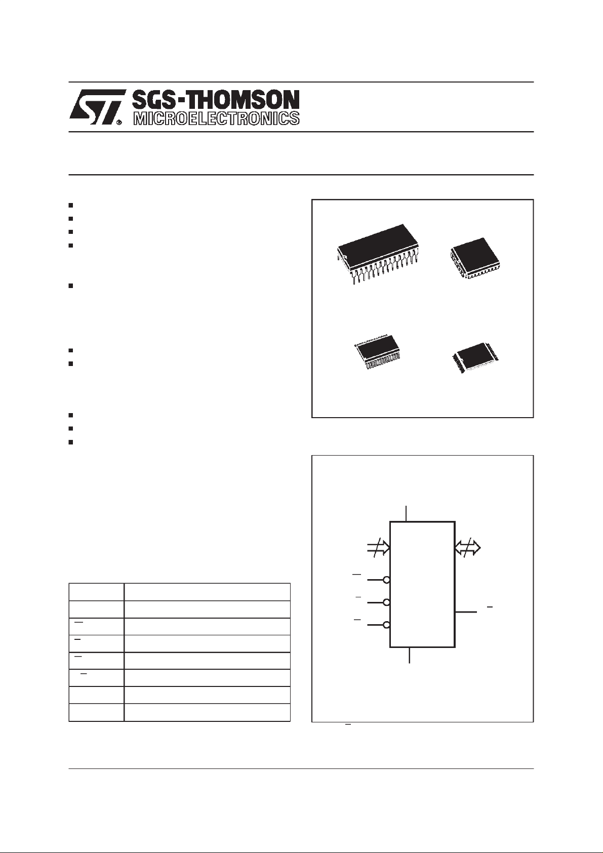
JEDECAPPROVEDBYTEWIDEPIN OUT
SOFTWARE DATAPROTECTION
TheM28LV64 is replacedby the
M28C64-xxW
28
1
PDIP28 (P) PLCC32 (K)
28
1
SO28 (MS)
300 mils
Figure 1. Logic Diagram
M28LV64
NOT FOR NEW DESIGN
TSOP28 (N)
8x13.4mm
DESCRIPTION
The M28LV64 is an 8K x 8 low power Parallel
EEPROM fabricated with SGS-THOMSON pro-
V
CC
prietary single polysilicon CMOS technology.The
device offersfast accesstime with low power dissipationand requiresa 2.7Vto 3.6Vpower supply.
A0-A12
Table 1. Signal Names
A0 - A12 Address Input
DQ0 - DQ7 Data Input / Output
W Write Enable
E Chip Enable
G Output Enable
RB Ready / Busy
V
CC
V
SS
May 1997 1/18
This isinformation on a product still in production but not recommended for new designs.
Supply Voltage
Ground
Note: * RB function is only available on the M28LV64.
W
13
M28LV64
E
G
V
SS
8
DQ0-DQ7
RB *
AI01538B
M28LV64
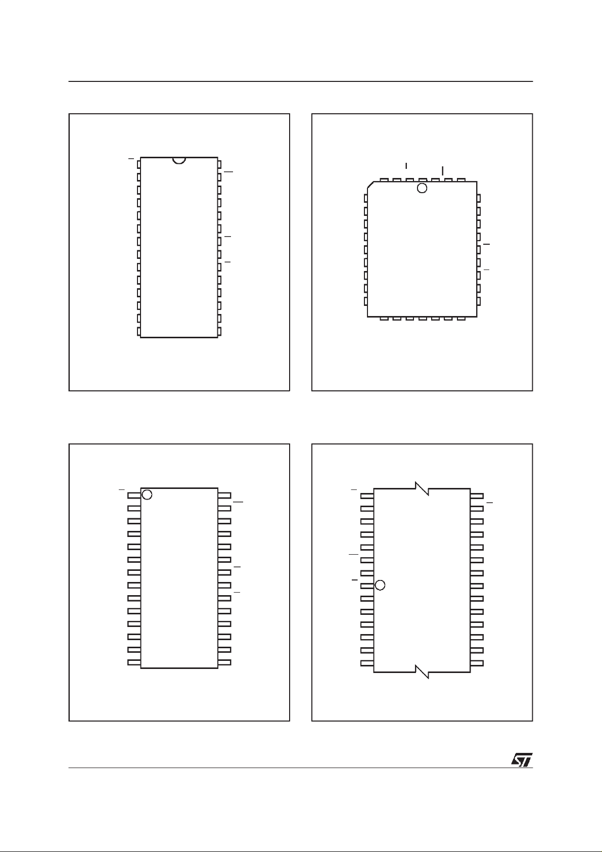
Figure2A. DIPPin Connections
RB V
1
A12
2
A7
3
A6
4
A5
5
A4
6
A3
7
8
9
10
11
M28LV64
A2
A1
A0
DQ0
12
DQ2
13
14
SS
Warning: NC =Not Connected.
28
27
26
25
24
23
22
21
20
19
18
17
16
15
AI01539B
CC
W
NC
A8
A9
A11
G
A10
E
DQ7
DQ6
DQ5DQ1
DQ4
DQ3V
Figure2B. LCC Pin Connections
CC
NC
DU
32
W
V
A8
A9
A11
NC
G
25
A10
E
DQ7
DQ6
DQ4
DQ5
AI01540B
RB
A7
A12
1
A6
A5
A4
A3
A2
9
M28LV64
A1
A0
NC
DQ0
17
SS
V
DQ1
DQ2DUDQ3
Warning: NC = Not Connected, DU = Don’t Use.
Figure2C. SO Pin Connections
RB
A12
DQ0
DQ1
DQ2
V
SS
Warning: NC =Not Connected.
A7
A6
A5
A4
A3
A2
A1
A0
1
2
3
4
5
6
7
M28LV64
8
9
10
11
12
13
14
28
27
26
25
24
23 A11
22
21
20
19
18
17
16
15
AI01541B
V
CC
W
NC
A8
A9
G
A10
E
DQ7
DQ6
DQ5
DQ4
DQ3
Figure2D. TSOPPin Connections
G
22
A11
A9
A8
NC
W
V
CC
RB
28
1
M28LV64
A12
A7
A6
A5
A4
A3
78
Warning: NC = Not Connected.
21
15
14
AI01542B
A10
E
DQ7
DQ6
DQ5
DQ4
DQ3
V
SS
DQ2
DQ1
DQ0
A0
A1
A2
2/18
M28LV64
Table 2. Absolute Maximum Ratings
(1)
Symbol Parameter Value Unit
T
A
T
STG
V
CC
V
IO
V
V
ESD
Notes: 1. Except for the rating ”Operating Temperature Range”, stresses above those listed in the Table ”Absolute Maximum Ratings” may
2. 100pF through1500Ω; MIL-STD-883C, 3015.7
Ambient Operating Temperature – 40 to 85 °C
Storage Temperature Range – 65 to 150 °C
Supply Voltage –0.3 to 6.5 V
Input/Output Voltage – 0.3 to VCC+0.6 V
Input Voltage –0.3 to 6.5 V
I
Electrostatic Discharge Voltage (Human Bodymodel)
cause permanent damage to the device. These are stress ratings only and operation ofthe deviceat these or any otherconditions
above thoseindicated in the Operating sections of this specification isnot implied. Exposure to Absolute Maximum Rating
conditions for extended periods mayaffect device reliability. Refer also to theSGS-THOMSON SURE Program and other
relevant quality documents.
(2)
4000 V
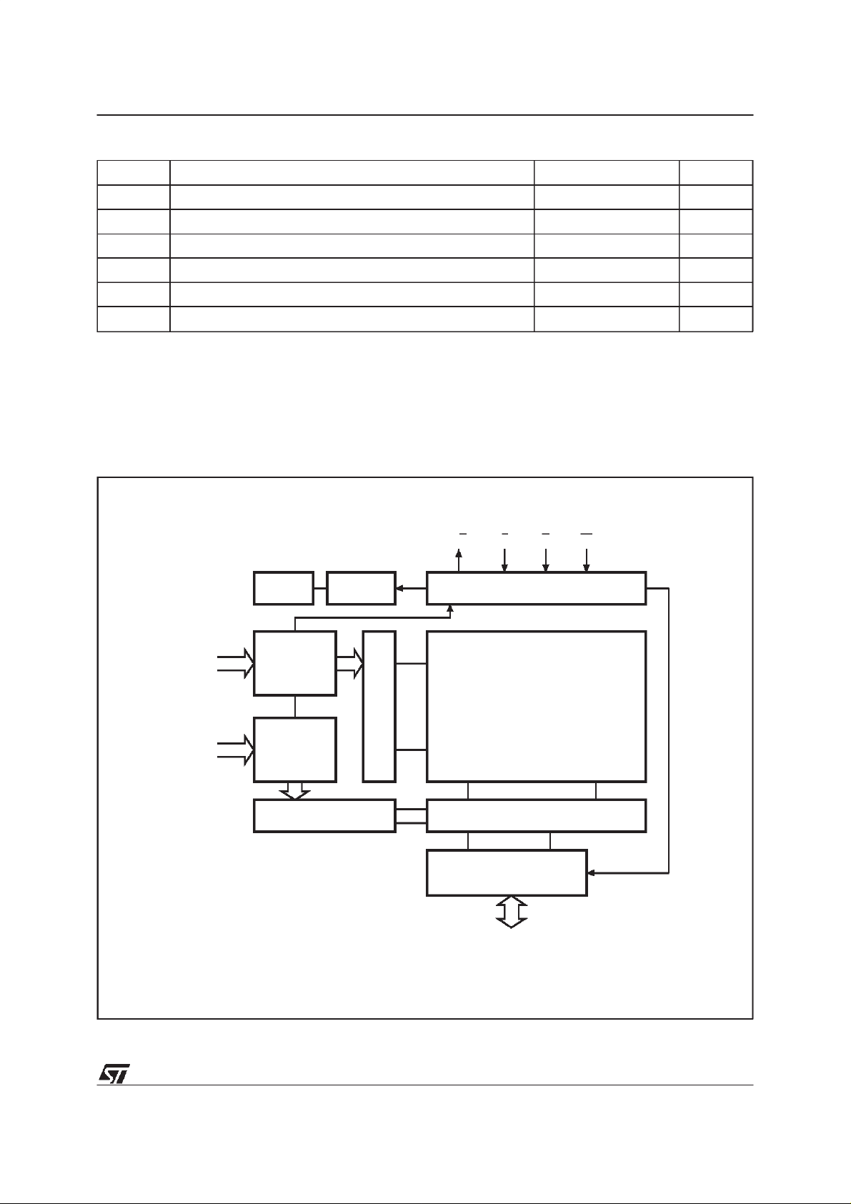
Figure3. Block Diagram
RB E G W
A6-A12
(Page Address)
A0-A5
VPPGEN RESET
ADDRESS
LATCH
ADDRESS
LATCH
Y DECODE
X DECODE
CONTROL LOGIC
64K ARRAY
SENSE ANDDATA LATCH
I/O BUFFERS
DQ0-DQ7
PAGE
LOAD
TIMER STATUS
TOGGLE BIT
DATA POLLING
AI01355
3/18

M28LV64
Table 3. Operating Modes
Mode E G W DQ0 - DQ7
Standby 1 X X Hi-Z
Output Disable X 1 X Hi-Z
Write Disable X X 1 Hi-Z
Read 0 0 1 Data Out
Write 0 1 0 Data In
Note: 1. 0 = VIL;1=VIH;X=VILor VIH.
DESCRIPTION (cont’d)
The M28LV64 outputs the Ready/Busy write
status,theM28LV64-aaaX(aaa=access time)has
no Ready/Busy status and the relevant RB pin is
Not Connected (NC). The circuit has been designed to offer a flexible microcontroller interface
featuring both hardware and software handshaking with Ready/Busy,Data Polling and ToggleBit.
The M28LV64supports 64byte page writeoperation. A Software Data Protection (SDP) is also
possibleusing the standard JEDECalgorithm.
(1)
OPERATION
In order topreventdata corruptionandinadvertent
writeoperationsan internalV
Write operation if V
is below VWI(see Table 6).
CC
comparatorinhibits
CC
Accesstothememory inwritemodeisallowedafter
a power-upas specifiedin Table6.
Read
TheM28LV64isaccessedlikea staticRAM. When
E and G are low with W high, the data addressed
ispresented on the I/O pins. The I/Opins are high
impedancewhen eitherG or E is high.
Write
PINDESCRIPTION
Addresses (A0-A12). The address inputs select
an 8-bit memory location during a read or write
operation.
Chip Enable (E). The chip enable input must be
lowto enableallread/writeoperations.When Chip
Enableis high, power consumptionis reduced.
OutputEnable (G). TheOutput Enableinput controls the data output buffers and is used to initiate
readoperations.
DataIn/Out (DQ0 - DQ7).Data iswritten toorread
fromthe M28LV64 throughthe I/O pins.
WriteEnable(W).The WriteEnableinputcontrols
the writing of data to the M28LV64.
Ready/Busy (RB). Ready/Busy is an open drain
output that can be used to detect the end of the
internalwritecycle(thisfunctionappliesonly tothe
M28LV64).
Write operationsare initiated when both W and E
are low andG is high.TheM28LV64supports both
E and W controlled write cycles. The Address is
latched by the falling edge of E or W which ever
occurslast andthe Dataon the rising edge of E or
W which ever occurs first. Once initiated the write
operationis internallytimed untilcompletion.
Page Write
Page write allows up to 64 bytes to be consecutively latched into the memory prior to initiating a
programmingcycle. Allbytes must be located in a
single page address, that is A6-A12 must be the
samefor all bytes. Thepage writecan beinitiated
duringany byte writeoperation.
Following the first byte write instruction the host
may send another address and data with a minimum data transfer rate of t
(see Figure 13).
WHWH
If atransitionofEor Wisnotdetectedwithin t
the internal programmingcycle will start.
WHWH
4/18
M28LV64
Microcontroller ControlInterface
The M28LV64provides two write operation status
bitsandonestatuspinthatcanbeusedto minimize
the system write cycle. Thesesignals are available
on the I/O port bits DQ7 or DQ6 of the memory
duringprogrammingcycleonly,oras theRBsignal
on a separatepin.
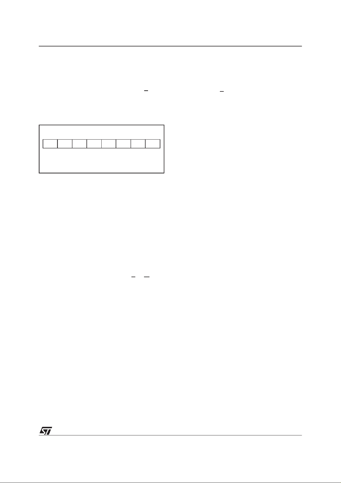
Figure4. Status Bit Assignment
DQ7 DQ6 DQ5 DQ4 DQ3 DQ2 DQ1 DQ0
DP TB PLTS Hi-Z Hi-Z Hi-Z Hi-Z Hi-Z
DP =Data Polling
TB = ToggleBit
PLTS = Page Load Timer Status
Data Polling bit (DQ7). During the internal write
cycle,any attempt to read the last bytewritten will
produce on DQ7 the complementary value of the
previouslylatched bit. Once the write cycle is finished the true logic value appears on DQ7 in the
readcycle.
Toggle bit (DQ6). The M28LV64 offers another
way for determiningwhen the internal write cycle
iscompleted.DuringtheinternalErase/Writecycle,
DQ6 will toggle from ”0” to ”1” and ”1” to ”0” (the
first read value is ”0”) on subsequent attempts to
read the memory. When the internalcycle is completed the togglingwill stopand the devicewill be
accessiblefor a new Read or Writeoperation.
Page Load Timer Status bit (DQ5). In the Page
Write mode data may be latched by E or W up to
100µs after theprevious byte. Upto 64bytes may
be input. The Data output (DQ5) indicates the
status of the internal Page Load Timer. DQ5 may
be read by asserting Output Enable Low (t
PLTS
DQ5 Low indicates the timer is running,High indicates time-out after which the write cyclewill start
and no new data may be input.
Ready/Busy p in (avail able only on the
M28LV64).TheRB pinprovidesa signalat itsopen
drain output which is low during the erase/write
cycle,butwhichis releasedatthecompletionof the
programmingcycle.
SoftwareData Protection
The M28LV64 offers a software controlled write
protection facility that allows the user to inhibit all
write modesto thedevice includingthe ChipErase
instruction. This can be useful in protecting the
memory from inadvertent write cycles that may
occurdue touncontrolled bus conditions.
The M28LV64isshippedasstandardinthe”unprotected” state meaning that the memory contents
can be changed as requiredby the user.After the
Software Data Protection enable algorithm is issued, the device enters the ”Protect Mode” of
operation where no further write commands have
any effect on the memory contents. The device
remains in this mode until a valid Software Data
Protection (SDP) disable sequence is received
whereby the device reverts to its ”unprotected”
state. The Software Data Protection is fully nonvolatile and is not changed by power on/off sequences.
Toenable the SoftwareData Protection(SDP) the
devicerequirestheusertowrite(withaPageWrite)
three specificdata bytes to three specificmemory
locations as per Figure 5. Similarly to disable the
Software Data Protection the user has to write
specificdata bytesintosixdifferentlocationsasper
Figure 6 (with a Page Write). This complexseries
ensures that the user will never enable or disable
the SoftwareData Protectionaccidentally.
).
5/18
M28LV64
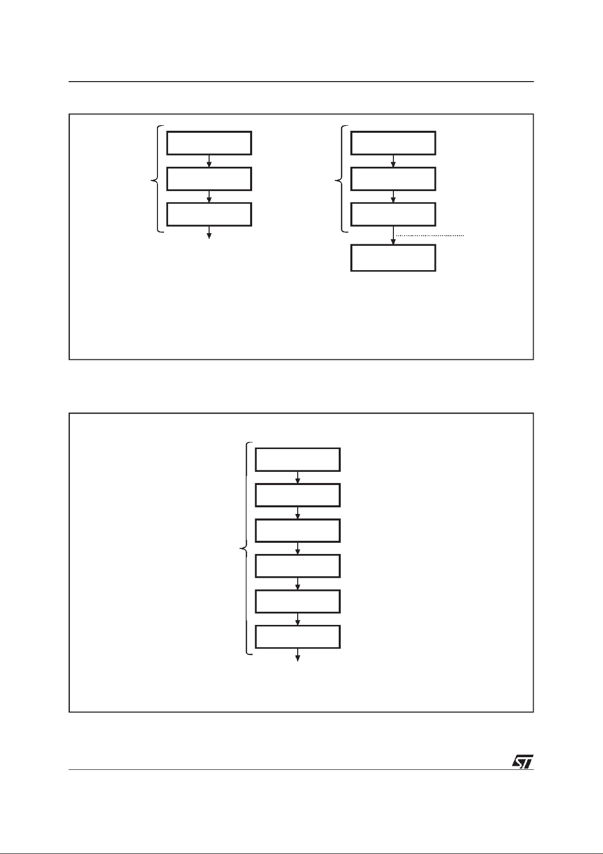
Figure5. Software DataProtection EnableAlgorithmand MemoryWrite
WRITE AAh in
Address 1555h
Page
Write
Instruction
(Note 1)
Note: 1.MSB Address bits (A6 to A12) differduringthese specific PageWrite operations.
WRITE 55h in
Address 0AAAh
WRITE A0h in
Address 1555h
SDP is set
SDP ENABLEALGORITHM
Page
Write
Instruction
(Note 1)
Figure6. Software DataProtection Disable Algorithm
WRITE AAh in
Address 1555h
WRITE 55h in
Address 0AAAh
WRITE A0h in
Address 1555h
Write
(1 up to 64 bytes)
WRITE IN
WHEN SDP IS SET
Page
MEMORY
AI01356B
WRITE
is enabled
Page
Write
Instruction
WRITE AAh in
Address 1555h
WRITE 55hin
Address 0AAAh
WRITE 80hin
Address 1555h
WRITE AAh in
Address 1555h
WRITE 55hin
Address 0AAAh
WRITE 20hin
Address 1555h
Unprotected State
AI01357
6/18
 Loading...