

M28F201
2 Mb (256K x 8, Chip Erase) FLASH MEMORY
April 1997 1/21
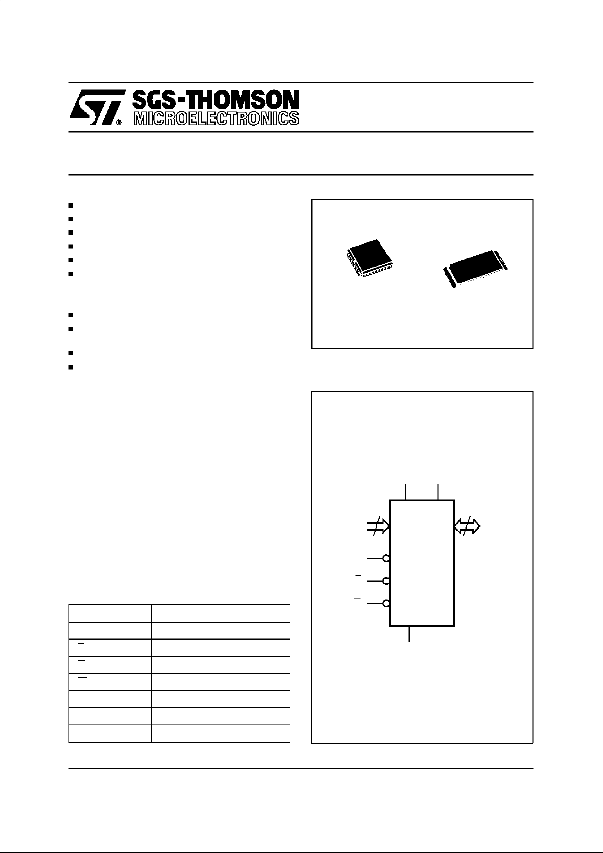
AI00637C
18
A0-A17
W
DQ0-DQ7
V
PP
V
CC
M28F201
G
E
V
SS
8
Figure 1. Logic Diagram
A0-A17 Address Inputs
DQ0-DQ7 Data Inputs / Outputs
E Chip Enable
G Output Enable
W Write Enable
V
PP
Program Supply
V
CC
SupplyVoltage
V
SS
Ground
Table 1. Signal Names
PLCC32 (K) TSOP32 (N)
8 x 20 mm
5V ± 10% SUPPLYVOLTAGE
12V PROGRAMMINGVOLTAGE
FASTACCESSTIME: 70ns
BYTEPROGRAMMINGTIME: 10µs typical
ELECTRICALCHIP ERASEin 1s RANGE
LOW POWERCONSUMPTION
– ActiveCurrent: 15mAtypical
– Stand-byCurrent: 10µAtypical
10,000PROGRAM/ERASE CYCLES
INTEGRATED ERASE/PROGRAM-STOP
TIMER
OTPCOMPATIBLE PACKAGESand PINOUTS
ELECTRONIC SIGNATURE
– ManufacturerCode: 20h
– DeviceCode: F4h
DESCRIPTION
The M28F201 FLASH Memory product is a nonvolatilememorieswhich may be erasedelectrically
at the chip level and programmed byte-by-byte. It
is organised as 256K bytes. It uses a command
registerarchitectureto select theoperating modes
and thus provide a simple microprocessor interface. The M28F201 FLASH Memory product is
suitablefor applicationswhere the memoryhas to
be reprogrammed in the equipment. The access
time of 70ns makes the device suitable for use in
high speed microprocessorsystems.
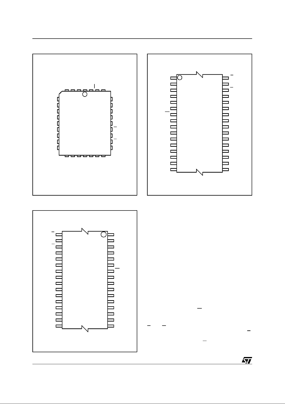
AI00638C
A17
A13
A10
DQ5
17
A1
A0
DQ0
DQ1
DQ2
DQ3
DQ4
A7
A4
A3
A2
A6
A5
9
W
A8
1
A16
A9
DQ7
A12
A14
32
VPPV
CC
M28F201
A15
A11
DQ6
G
E
25
V
SS
Figure2A. LCCPin Connections
A1
A0
DQ0
A7
A4 A3
A2
A6
A5
A13
A10
A8
A9
DQ7
A14
A11 G
E
DQ5
DQ1
DQ2
DQ3
DQ4
DQ6
A17
W
A16
A12
V
PP
V
CC
A15
AI00639C
M28F201
(Normal)
8
1
9
16 17
24
25
32
V
SS
Figure 2B. TSOPPin Connections
DEVICEOPERATION
TheM28F201 FLASHMemory product employsa
technologysimilar to a 2 Megabit EPROM but add
to the device functionality by providing electrical
erasure and programming. These functions are
managed by a command register. The functions
that are addressed via the command register depend on the voltage applied to the V
PP
, program
voltage, input. When V
PP
is less than or equal to
6.5V, the command register is disabled and the
M28F201functionsas a readonly memoryproviding operating modessimilar to anEPROM (Read,
Output Disable, Electronic Signature Read and
Standby).WhenV
PP
israisedto 12Vthecommand
register is enabled and this provides, in addition,
Eraseand Program operations.
READONLYMODES, V
PP
≤ 6.5V
For all Read Only Modes, except StandbyMode,
the Write Enable input W should be High. In the
StandbyMode this input is ’don’tcare’.
ReadMode. TheM28F201has twoenableinputs,
E and G, both of which must be Low in order to
outputdata from thememory. TheChipEnable(E)
isthe powercontroland shouldbe usedfor device
selection. Output Enable (G) is the output control
and should be used to gatedata on to the output,
independantof the deviceselection.
A1
A0
DQ0
A7
A4A3
A2
A6
A5
A13
A10
A8
A9
DQ7
A14
A11G
E
DQ5
DQ1
DQ2
DQ3
DQ4
DQ6
A17
W
A16
A12
V
PP
V
CC
A15
AI00640D
M28F201
(Reverse)
8
9
16 17
24
25
V
SS
321
Figure2C. TSOPReverse Pin Connections
2/21
M28F201
Symbol Parameter Value Unit
T
A
Ambient Operating Temperature –40 to125 °C
T
STG
Storage Temperature –65 to150 °C
V
IO
Input or Output Voltages –0.6 to 7 V
V
CC
Supply Voltage –0.6 to 7 V
V
A9
A9 Voltage –0.6 to 13.5 V
V
PP
Program Supply Voltage, during Erase
or Programming
–0.6 to 14 V
Note: Except for therating ”Operating Temperature Range”, stressesabove those listed in the Table”AbsoluteMaximum Ratings” may
cause permanent damage tothe device. These are stress ratings onlyand operation of the device at these or any other conditions above
those indicated in the Operating sections of this specificationis notimplied. Exposure to AbsoluteMaximum Ratingconditions for extended
periods may affect device reliability.Refer also to the SGS-THOMSON SURE Program and otherrelevant quality documents.
Table 2. AbsoluteMaximumRatings
Identifier A0 DQ7 DQ6 DQ5 DQ4 DQ3 DQ2 DQ1 DQ0 Hex Data
Manufacturer’s Code V
IL
00100000 20h
Device Code V
IH
11110100 F4h
Table 4. Electronic Signature
V
PP
Operation E G W A9 DQ0 - DQ7
ReadOnly V
PPL
Read V
IL
V
IL
V
IH
A9 Data Output
Output Disable V
IL
V
IH
V
IH
X Hi-Z
Standby V
IH
X X X Hi-Z
Electronic Signature V
IL
V
IL
V
IH
V
ID
Codes
Read/Write
(2)
V
PPH
Read V
IL
V
IL
V
IH
A9 Data Output
Write V
IL
V
IH
VILPulse A9 Data Input
Output Disable V
IL
V
IH
V
IH
X Hi-Z
Standby V
IH
X X X Hi-Z
Notes: 1. X = VILor VIH.
2. Refer also to the Command table.
Table 3. Operations
(1)
3/21
M28F201
Command Cycles
1st Cycle 2nd Cycle
Operation A0-A17 DQ0-DQ7 Operation A0-A17 DQ0-DQ7
Read 1 Write X 00h
Electronic
Signature
(2)
2 Write X 80h or 90h
Read 00000h 20h
Read 00001h F4h
Setup Erase/
2
Write X 20h
Erase Write X 20h
Erase Verify 2 Write A0-A17 A0h Read X Data Output
Setup Program/
2
Write X 40h
Program Write A0-A17 Data Input
Program Verify 2 Write X C0h Read X Data Output
Reset 2 Write X FFh Write X FFh
Notes: 1. X = VILor VIH.
2. Refer also to the Electronic Signaturetable.
Table 5. Commands
(1)
Standby Mode. In the Standby Mode the maxi-
mum supply current is reduced. The device is
placed in the Standby Mode by applying a High
level to the Chip Enable (E) input. When in the
StandbyModetheoutputsare ina highimpedance
state, independantof theOutput Enable (G)input.
Output Disable Mode. When the Output Enable
(G) is High the outputs are in a high impedance
state.
ElectronicSignatureMode.Thismodeallowsthe
readout of two binary codesfromthe device which
identify the manufacturer and device type. This
mode is intended for use by programming equipment to automaticallyselect the correct eraseand
programmingalgorithms.The ElectronicSignature
Mode is activewhen a highvoltage (11.5Vto 13V)
isapplied toaddresslineA9withEandG Low.With
A0 Low the output data is the manufacturercode,
when A0 isHigh the output is thedevice code. All
other address lines should be maintained Low
while reading the codes. The electronicsignature
canalso be accessed in Read/Writemodes.
READ/WRITE MODES, 11.4V≤ V
PP
≤12.6V
When V
PP
is High both read and write operations
may be performed. These are defined by thecontents ofan internalcommand register.Commands
may be written to this register to set-up and execute,Erase,EraseVerify,Program,Program Verify
and Reset modes. Each of these modes needs 2
cycles. Each mode starts with a write operationto
set-upthe command,thisis followedby eitherread
or write operations. The device expects the first
cycle to be a write operation and doesnot corrupt
data at any location in the memory.Read modeis
set-upwith one cycle onlyand maybe followedby
any number of read operations to output data.
ElectronicSignatureRead modeis set-upwithone
cycle and followed by a read cycle to output the
manufactureror device codes.
Awriteto thecommandregisterismadebybringing
WLowwhileEisLow.ThefallingedgeofWlatches
Addresses, while the rising edge latches Data,
which are used for those commands that require
address inputs, command input or provide data
output. The supply voltage V
CC
and the program
voltageV
PP
canbe applied in any order. Whenthe
device is powered up or when V
PP
is ≤ 6.5V the
contentsof thecommand register defaultsto 00h,
thus automatically setting-up Read operations. In
addition a specific command may be used to set
the commandregisterto 00h for readingthe memory. The system designer may chose to provide a
constanthigh V
PP
anduse the registercommands
for all operations,or to switch the V
PP
from low to
high only when needing to erase or program the
memory. All command registeraccess is inhibited
whenV
CC
fallsbelowthe Erase/WriteLockoutVolt-
age (V
LKO
) of 2.5V.
If the device is deselected during Erasure, Programming or verifying it will draw active supply
currentsuntil the operationsare terminated.
The device is protected against stress caused by
long erase or programtimes.If theend ofErase or
Programming operations are not terminated by a
Verifycycle within a maximumtime permitted, an
internal stop timer automatically stops the operation.The deviceremainsin aninactivestate, ready
to start a Verifyor ResetMode operation.
4/21
M28F201
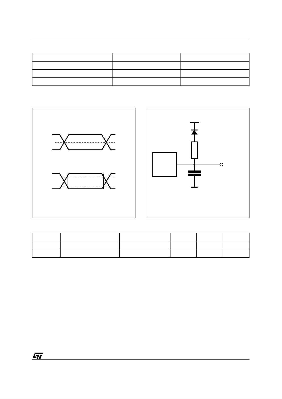
SRAM Interface Levels EPROM Interface Levels
Input Rise and Fall Times ≤ 10ns ≤ 10ns
Input PulseVoltages 0 to 3V 0.45V to 2.4V
Input and Output Timing Ref. Voltages 1.5V 0.8Vand 2V
Table 6. AC Measurement Conditions
AI01275
3V
SRAM Interface
0V
1.5V
2.4V
EPROM Interface
0.45V
2.0V
0.8V
Figure3. AC Testing Input Output Waveform
AI01276
1.3V
OUT
CL= 30pF or 100pF
CL= 30pF for SRAM Interface
CL= 100pF for EPROM Interface
CLincludes JIG capacitance
3.3kΩ
1N914
DEVICE
UNDER
TEST
Figure4. AC Testing Load Circuit
Symbol Parameter TestCondition Min Max Unit
C
IN
Input Capacitance VIN=0V 6 pF
C
OUT
Output Capacitance V
OUT
=0V 12 pF
Note: 1. Sampled only, not 100% tested.
Table 7. Capacitance
(1)
(TA=25°C, f = 1 MHz )
Read Mode. The Read Mode is the default at
power up or may be set-up by writing 00h to the
command register. Subsequent read operations
outputdatafromthememory.Thememoryremains
in the Read Mode until a new command is written
to the commandregister.
ElectronicSignatureMode. Inorder to select the
correcterase and programmingalgorithmsfor onboard programming,the manufacturerand device
codesmay be read directly. It isnot neccessaryto
apply a high voltage to A9 when using the command register. The Electronic Signature Mode is
set-up by writing 80h or 90h to the command
register. The following read cycles, with address
inputs00000hor 00001h,outputthe manufacturer
or device codes. The command is terminated by
writing another valid command to the command
register(for exampleReset).
5/21
M28F201
Symbol Parameter Test Condition Min Max Unit
I
LI
Input LeakageCurrent 0V ≤ VIN≤ V
CC
±1 µA
I
LO
Output Leakage Current 0V ≤ V
OUT
≤ V
CC
±10 µA
I
CC
Supply Current (Read) E = VIL, f = 10MHz 30 mA
I
CC1
Supply Current (Standby) TTL E = V
IH
1mA
Supply Current (Standby) CMOS E = V
CC
± 0.2V 100 µA
I
CC2
(1)
Supply Current (Programming) During Programming 10 mA
I
CC3
(1)
Supply Current (Program Verify) During Verify 20 mA
I
CC4
(1)
Supply Current (Erase) During Erasure 20 mA
I
CC5
(1)
Supply Current (Erase Verify) During Erase Verify) 20 mA
I
LPP
Program Leakage Current VPP≤ V
CC
±10 µA
I
PP
Program Current (Read or
Standby)
V
PP>VCC
200 µA
V
PP
≤ V
CC
±10 µA
I
PP1
(1)
Program Current (Programming) VPP=V
PPH
, During Programming 30 mA
I
PP2
(1)
Program Current (Program
Verify)
V
PP=VPPH
, During Verify 5 mA
I
PP3
(1)
Program Current (Erase) VPP=V
PPH
, During Erase 30 mA
I
PP4
(1)
Program Current (Erase Verify) VPP=V
PPH
, DuringErase Verify 5 mA
V
IL
Input Low Voltage –0.5 0.8 V
V
IH
Input High VoltageTTL 2 VCC+ 0.5 V
Input High Voltage CMOS 0.7 V
CC
VCC+ 0.5 V
V
OL
Output Low Voltage IOL= 5.8mA 0.45 V
V
OH
Output High Voltage CMOS
I
OH
= –100µAV
CC
– 0.4 V
I
OH
= –2.5mA 0.85 V
CC
V
Output High VoltageTTL I
OH
= –2.5mA 2.4 V
V
PPL
Program Voltage(Read
Operations)
0 6.5 V
V
PPH
Program Voltage(Read/Write
Operations)
11.4 12.6 V
V
ID
A9 Voltage(Electronic Signature) 11.5 13 V
I
ID
(1)
A9 Current (Electronic Signature) A9 = V
ID
200 µA
V
LKO
Supply Voltage,Erase/Program
Lock-out
2.5 V
Note: 1. Not 100% tested. Characterisation Data available.
Table 8. DC Characteristics
(T
A
= 0 to 70 °C, –40 to 85 °C or –40to 125 °C; VCC=5V±10%)
6/21
M28F201
Symbol Alt Parameter Test Condition
M28F201
Unit
-70 -90 -120 -150
V
CC
=
5V±10%
VCC=
5V±10%
VCC=
5V±10%
VCC=
5V±10%
EPROM
Interface
EPROM
Interface
EPROM
Interface
EPROM
Interface
Min Max Min Max Min Max Min Max
t
WHGL
Write Enable High to
Output EnableLow
6666µs
t
AVAV
t
RC
Read Cycle Time E = VIL,G=VIL70 90 120 150 ns
t
AVQV
t
ACC
Address Validto
Output Valid
E=V
IL
,G=V
IL
70 90 120 150 ns
t
ELQX
(1)
t
LZ
Chip Enable Low to
Output Transition
G=V
IL
0000ns
t
ELQV
t
CE
Chip Enable Low to
Output Valid
G=V
IL
70 90 120 150 ns
t
GLQX
(1)
t
OLZ
Output EnableLow
to Output Transition
E=V
IL
0000ns
t
GLQV
t
OE
Output EnableLow
to Output Valid
E=V
IL
25 30 35 40 ns
t
EHQZ
(1)
Chip Enable High to
Output Hi-Z
G=V
IL
0 25 0 30 0 30 0 35 ns
t
GHQZ
(1)
t
DF
Output EnableHigh
to Output Hi-Z
E=V
IL
0 25 0 30 0 30 0 35 ns
t
AXQX
t
OH
Address Transition
to Output Transition
E=V
IL
,G=VIL0000ns
Note: 1. Sampled only,not 100% tested
Table9. Read Only Mode AC Characteristics
((T
A
= 0 to 70 °C, –40 to 85 °C or –40 to 125 °C)
Erase and Erase Verify Modes. The memory is
erased by first Programming all bytes to 00h,the
Erase command then erases them to FFh. The
Erase Verify command is then used to read the
memory byte-by-byte for a content of FFh. The
Erase Mode is set-up by writing 20h to the command register. The write cycle is then repeated to
start the erase operation. Erasure starts on the
rising edge of W duringthis second cycle.Eraseis
followed by an Erase Verify which reads an addressed byte. Erase VerifyMode is set-up bywriting A0h tothe command register and at thesame
time supplying the address of the byte to be verified. The rising edge of W duringthe set-up of the
firstErase VerifyMode stops theEraseoperation.
Thefollowing read cycle is madewith an internally
generated margin voltage applied; reading FFh
indicatesthatallbitsof theaddressedbyte arefully
erased. The whole contents of the memory are
verified by repeating the Erase Verify Operation,
first writing the set-up code A0h with the address
of thebyte to be verified and thenreadingthe byte
contentsin a secondread cycle.
As the Erasealgorithm flow chart shows,when the
data read during Erase Verify is not FFh, another
Eraseoperation is performedand verificationcontinuesfromtheaddressofthelast verifiedbyte.The
command is terminated by writing another valid
command to the command register (for example
Programor Reset).
7/21
M28F201
 Loading...