

SGS Thomson Microelectronics M28F101-120N1, M28F101-100P1, M28F101-150P6, M28F101-150P1, M28F101-150K1 Datasheet
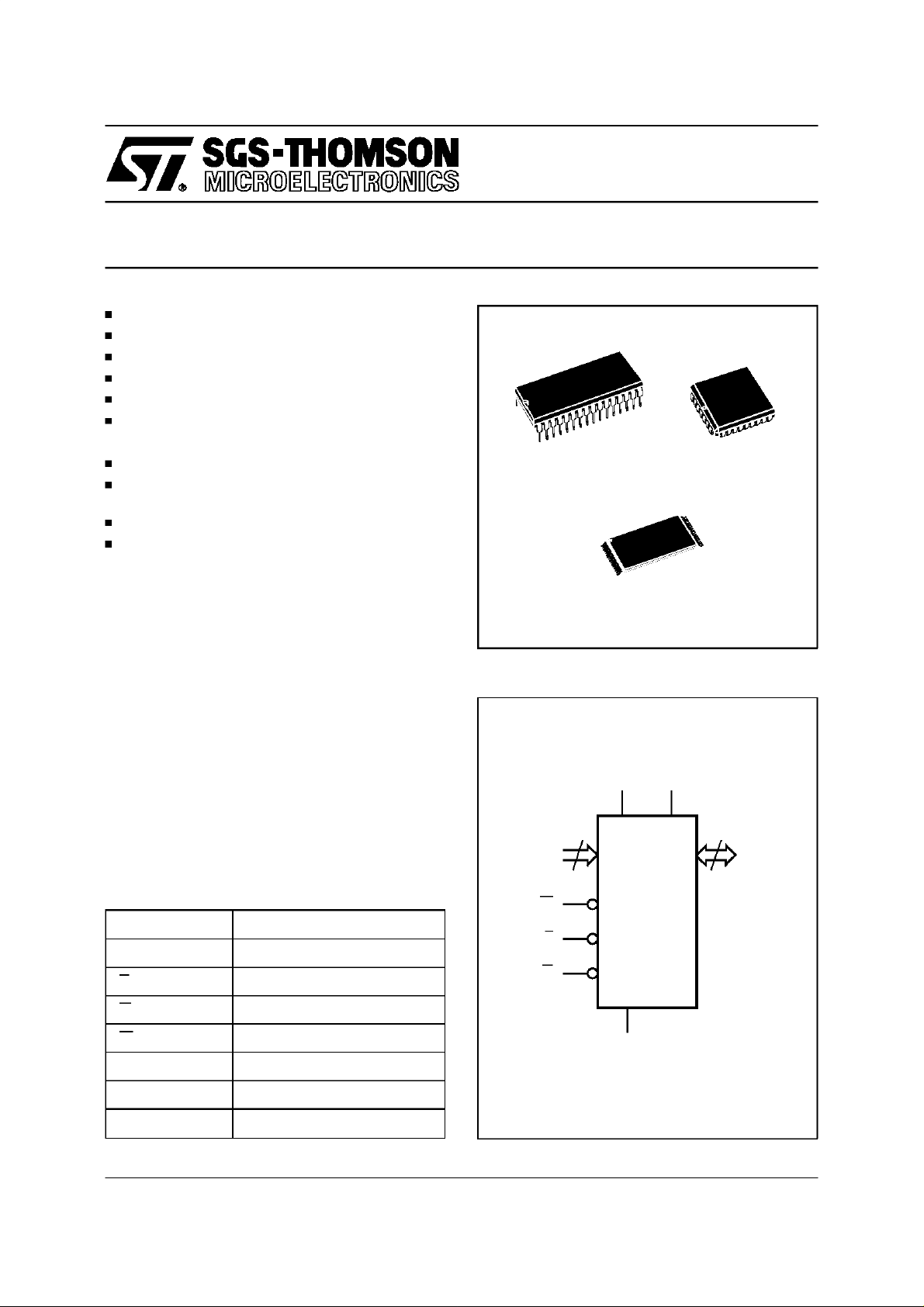
1 Mb (128K x 8, Chip Erase) FLASH MEMORY
5V ±10% SUPPLY VOLTAGE
12V PROGRAMMINGVOLTAGE
FASTACCESSTIME: 70ns
BYTEPROGRAMINGTIME: 10µs typical
ELECTRICALCHIP ERASE in 1s RANGE
LOW POWERCONSUMPTION
– Stand-byCurrent: 100µAmax
10,000ERASE/PROGRAM CYCLES
INTEGRATED ERASE/PROGRAM-STOP
TIMER
OTPCOMPATIBLE PACKAGESand PINOUTS
ELECTRONIC SIGNATURE
– ManufacturerCode: 20h
– DeviceCode: 07h
DESCRIPTION
The M28F101 FLASH Memory is a non-volatile
memory which may be erased electrically at the
chip level and programmed byte-by-byte. It is organisedas128K bytesof8 bits.It usesacommand
registerarchitectureto select the operating modes
and thus provides a simple microprocessor interface.The M28F101 FLASHMemory is suitablefor
applications where the memory has to be reprogrammed in the equipment. The access time of
70ns makes the device suitable for use in high
speedmicroprocessor systems.
32
1
PDIP32 (P)
TSOP32 (N)
8 x 20 mm
Figure 1. Logic Diagram
V
CC
17
A0-A16
M28F101
PLCC32 (K)
V
PP
8
DQ0-DQ7
Table 1. Signal Names
A0-A16 Address Inputs
DQ0-DQ7 Data Inputs / Outputs
E Chip Enable
G Output Enable
W Write Enable
V
PP
V
CC
V
SS
April 1997 1/23
Program Supply
SupplyVoltage
Ground
W
M28F101
E
G
V
SS
AI00666B
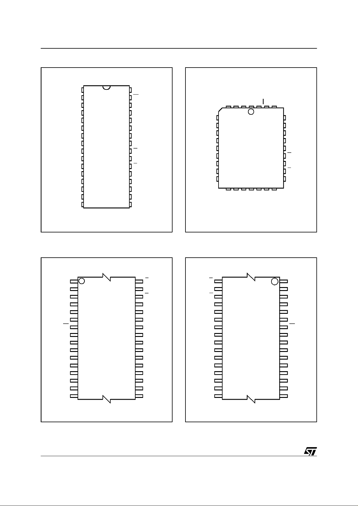
M28F101
Figure2A. DIP Pin Connections
V
1
PP
2
A15
3
A12
4
A7
5
A6
6
A5
7
A4
8
9
10
11
12
13
M28F101
A3
A2
A1
A0
DQ0
14
DQ2
15
16
SS
Warning: NC = Not Connected. Warning: NC = Not Connected.
32
31
30
29
28
27
26
25
24
23
22
21
20
19
18
17
AI00667
V
CC
WA16
NC
A14
A13
A8
A9
A11
G
A10
E
DQ7
DQ6
DQ5DQ1
DQ4
DQ3V
Figure2B. LCC Pin Connections
A16
A7
A6
A5
A4
A3
A2
A1
A0
DQ0
A12
9
DQ1
VPPV
A15
1
M28F101
17
SS
V
DQ2
DQ3
32
CC
DQ4
W
DQ5
NC
25
DQ6
A14
A13
A8
A9
A11
G
A10
E
DQ7
AI00668
Figure2C. TSOP Pin Connections
A11 G
A9
A8
A13
A14
NC
V
CC
V
PP
A16
A15
A12
A7
A6
A5
A4 A3
Warning: NC = Not Connected.
1
W
8
9
16 17
M28F101
(Normal)
32
25
24
AI00669B
A10
E
DQ7
DQ6
DQ5
DQ4
DQ3
V
SS
DQ2
DQ1
DQ0
A0
A1
A2
Figure2D. TSOP Reverse Pin Connections
1
A10
E
DQ7
DQ6
DQ5
DQ4
DQ3
V
SS
8
9
M28F101
(Reverse)
DQ2
DQ1
DQ0
A0
A1
A2
16 17
Warning: NC = Not Connected.
AI00670C
32
25
24
A11G
A9
A8
A13
A14
NC
W
V
CC
V
PP
A16
A15
A12
A7
A6
A5
A4A3
2/23
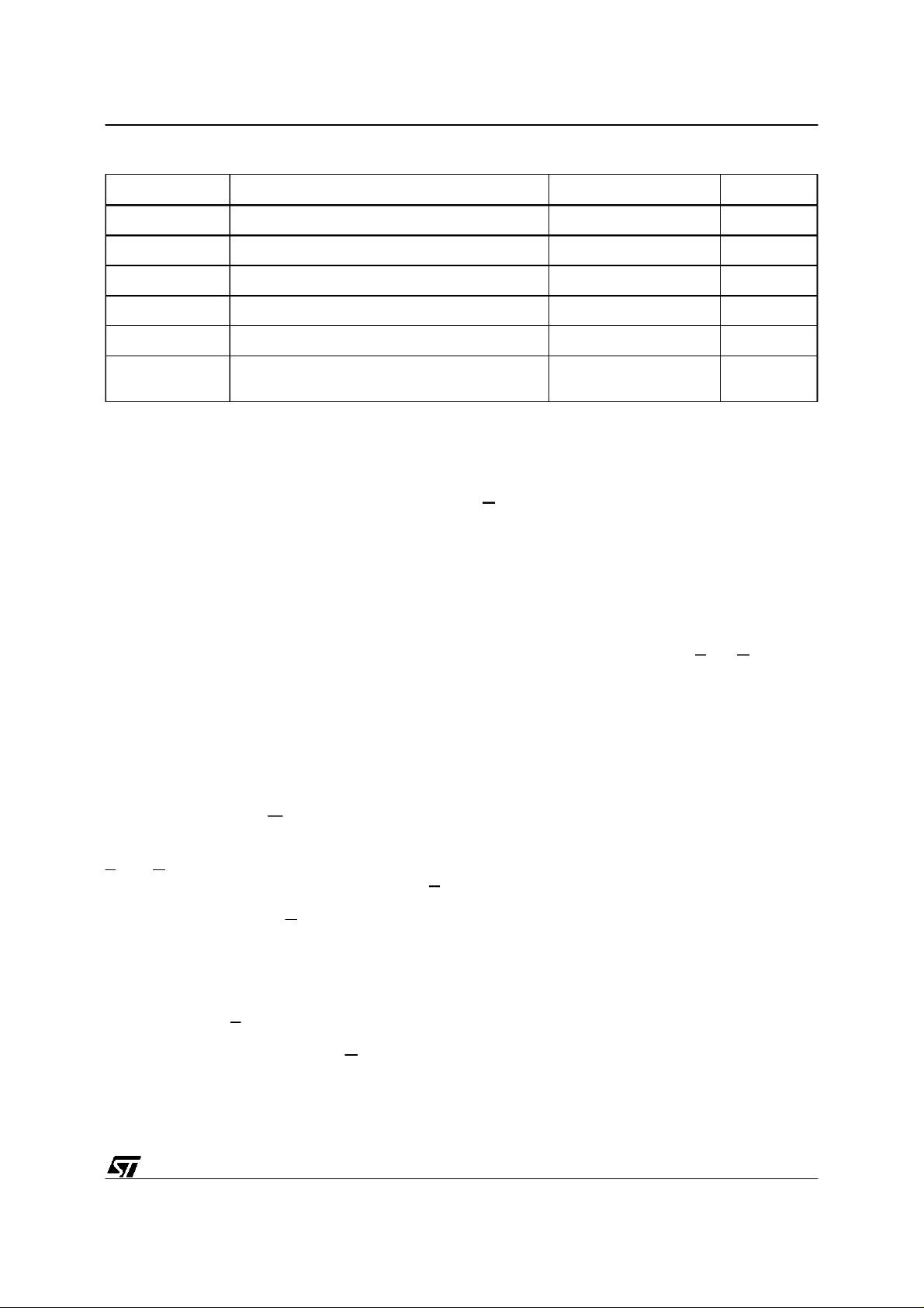
Table 2. AbsoluteMaximumRatings
Symbol Parameter Value Unit
M28F101
T
A
T
STG
V
IO
V
CC
V
A9
V
PP
Note: Except for therating ”Operating Temperature Range”, stressesabove those listed in the Table”Absolute Maximum Ratings” may
cause permanent damage to the device. These are stress ratings only and operation ofthe device at these or any otherconditions above
those indicated in the Operating sections of this specification is not implied. Exposure to Absolute Maximum Rating conditions for extended
periods may affect device reliability.Refer also to the SGS-THOMSON SURE Program and other relevant quality documents.
DEVICE OPERATION
The M28F101FLASHMemoryemploys a technologysimilar to a 1 MegabitEPROMbut adds to the
devicefunctionalityby providingelectrical erasure
and programming. These functions are managed
by a command register. The functions that are
addressed via the command register depend on
the voltage applied to the V
input. When V
commandregisteris disabled and M28F101functions as a read only memory providing operating
modes similar to an EPROM (Read, Output Disable, Electronic Signature Read and Standby).
When V
is raised to 12V the command regsiter
PP
isenabledand this provides,inaddition,Eraseand
Programoperations.
Ambient Operating Temperature –40 to 125 °C
Storage Temperature –65 to150 °C
Input or Output Voltages –0.6 to 7 V
Supply Voltage –0.6 to 7 V
A9 Voltage –0.6 to 13.5 V
Program Supply Voltage, during Erase
or Programming
–0.6 to 14 V
Output Disable Mode. When the Output Enable
(G) is High the outputs are in a high impedance
state.
ElectronicSignatureMode.Thismodeallowsthe
read outof two binarycodesfrom thedevice which
identify the manufacturer and device type. This
mode is intended for use by programming equip-
, program voltage,
is less than or equal to 6.5V,the
PP
PP
mentto automaticallyselect the correct erase and
programmingalgorithms.TheElectronicSignature
Modeis activewhen a high voltage (11.5Vto 13V)
isappliedto addresslineA9with EandG Low.With
A0 Low the output data is the manufacturercode,
whenA0 isHigh the outputis the devicetype code.
All other address lines should be maintained Low
while reading the codes. The electronicsignature
may also be accessedin Read/Write modes.
READONLYMODES, V
PP
≤ 6.5V
For all Read Only Modes, except Standby Mode,
the Write Enable input W should be High. In the
StandbyMode this input is don’t care.
ReadMode. TheM28F101has two enable inputs,
E and G, both of which must be Low in order to
output data from the memory. TheChipEnable (E)
is the powercontrol and shouldbe used for device
selection. Output Enable (G) is the output control
and should be used to gate data on to the output,
independantof the deviceselection.
Standby Mode. In the Standby Mode the maximum supply current is reduced. The device is
placedin the StandbyMode by applyinga High to
the Chip Enable (E) input. When in the Standby
Mode the outputs are in a high impedance state,
independantof the OutputEnable (G) input.
READ/WRITEMODES, 11.4V ≤ V
When V
is High both read and write operations
PP
≤ 12.6V
PP
may be performed. These are defined by the contents of an internal commandregister.Commands
may be written to this register to set-up and execute,Erase,EraseVerify,Program,ProgramVerify
and Reset modes. Each of these modes needs 2
cycles. Eah mode starts with a write operation to
set-upthe command,this is followedbyeither read
or write operations. The device expects the first
cycle to be a writeoperation and does not corrupt
data at any location in the memory.Read mode is
set-upwith one cycleonly and may be followed by
any number of read operations to output data.
ElectronicSignatureRead modeis set-up with one
cycle and followed by a read cycle to output the
manufactureror devicecodes.
3/23
M28F101
Table 3. Operations
ReadOnly V
(1)
V
PP
PPL
Operation E G W A9 DQ0 - DQ7
Output Disable V
Electronic Signature V
(2)
Read/Write
V
PPH
Output Disable V
Notes: 1. X = VILor VIH.
2. Refer also tothe Command table.
Table4. Electronic Signature
Identifier A0 DQ7 DQ6 DQ5 DQ4 DQ3 DQ2 DQ1 DQ0 Hex Data
Manufacturer’s Code V
Device Code V
IL
IH
Read V
Standby V
Read V
Write V
Standby V
IL
IL
IH
IL
IL
IL
IL
IH
V
IL
V
IH
V
IH
V
IH
A9 Data Output
X Hi-Z
X X X Hi-Z
V
IL
V
IL
V
IH
V
IH
V
IH
V
IH
V
ID
Codes
A9 Data Output
VILPulse A9 Data Input
V
IH
X Hi-Z
X X X Hi-Z
00100000 20h
00000111 07h
Table 5. Commands
Command Cycles
(1)
1st Cycle 2nd Cycle
Operation A0-A16 DQ0-DQ7 Operation A0-A16 DQ0-DQ7
Read 1 Write X 00h
Electronic
Signature
(2)
Setup Erase/
2 Write X 90h
2
Write X 20h
Read 00000h 20h
Read 00001h 07h
Erase Write X 20h
Erase Verify 2 Write A0-A16 A0h Read X Data Output
Setup Program/
2
Write X 40h
Program Write A0-A16 Data Input
Program Verify 2 Write X C0h Read X Data Output
Reset 2 Write X FFh Write X FFh
Notes: 1. X= VILor VIH.
2. Refer also to the Electronic Signature table.
4/23
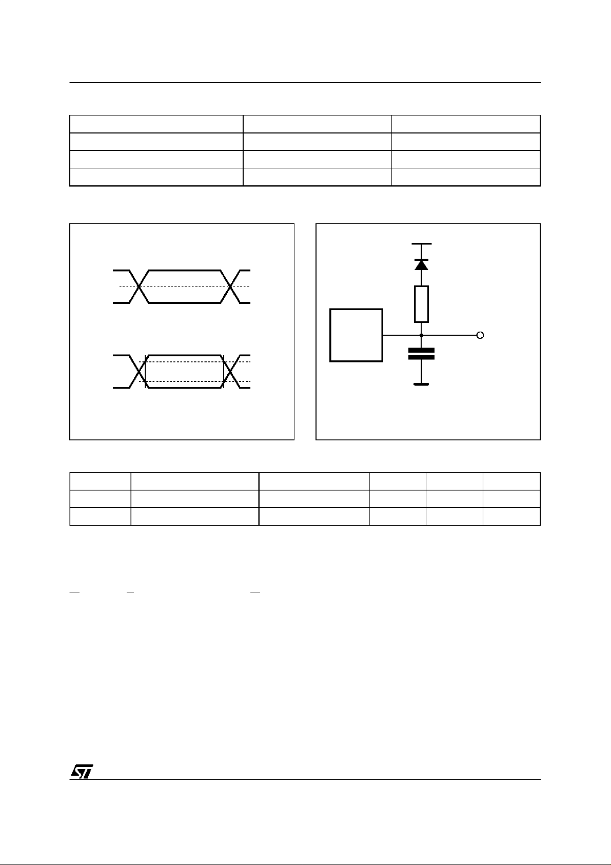
Table6. AC MeasurementConditions
SRAM Interface Levels EPROM Interface Levels
Input Rise and Fall Times ≤ 10ns ≤ 10ns
Input Pulse Voltages 0 to 3V 0.45V to 2.4V
Input and Output Timing Ref. Voltages 1.5V 0.8V and 2V
M28F101
Figure 3. AC TestingInput Output Waveform
SRAM Interface
3V
1.5V
0V
EPROM Interface
2.4V
0.45V
Table 7. Capacitance
Symbol Parameter Test Condition Min Max Unit
C
IN
C
OUT
Note: 1. Sampled only, not 100% test.ed
Input Capacitance VIN=0V 6 pF
Output Capacitance V
(1)
(TA=25°C, f = 1 MHz )
2.0V
0.8V
AI01275
Figure 4. ACTesting Load Circuit
1.3V
1N914
3.3kΩ
DEVICE
UNDER
TEST
CL= 30pF or 100pF
CL= 30pF for SRAM Interface
CL= 100pF for EPROM Interface
CLincludes JIG capacitance
=0V 12 pF
OUT
OUT
AI01276
READ/WRITE MODES (cont’d)
Awritetothecommandregisterismadebybringing
WLowwhileEisLow.ThefallingedgeofW latches
Addresses, while the rising edge latches Data,
which are used for those commands that require
address inputs, command input or provide data
output.
The supply voltage V
canbe applied in any order. When the device
V
PP
is powered up or when V
and the program voltage
CC
is ≤ 6.5V the contents
PP
of the command register defaults to 00h, thus
automaticallysetting-up Read operations. In addition a specific command may be used to set the
commandregister to 00h for reading the memory.
Thesystem designer may chose to provide a constanthigh V
all operations,or toswitchthe V
and use the register commands for
PP
fromlow to high
PP
only when needing to eraseor program the memory. Allcommandregisteraccess isinhibited when
falls below the Erase/Write Lockout Voltage
V
CC
) of 2.5V.
(V
LKO
If the device is deselected during Erasure, Programmingor Verification it will draw active supply
currentsuntil the operations are terminated.
The device is protected against stress caused by
long erase or program times. If the end of Erase or
Programming operations are not terminated by a
Verifycycle within a maximum time permitted, an
internal stop timer automatically stops the operation.The deviceremainsin an inactivestate, ready
to start a Verifyor ResetMode operation.
5/23
M28F101
Table8. DC Characteristics
= 0 to 70°C, –40to 85 °C or–40 to 125 °C;VCC=5V±10%)
(T
A
Symbol Parameter TestCondition Min Max Unit
I
I
LO
I
CC
I
CC1
I
CC2
I
CC3
I
CC4
I
CC5
I
LPP
I
PP
I
PP1
I
PP2
I
PP3
I
PP4
V
V
V
V
OH
V
PPL
V
PPH
V
I
ID
V
LKO
Note: 1. Not 100% tested.Characterisation Data available.
Input Leakage Current 0V ≤ VIN≤ V
LI
Output Leakage Current 0V ≤ V
OUT
≤ V
CC
CC
Supply Current (Read) E = VIL, f = 6MHz 30 mA
Supply Current (Standby) TTL E = V
Supply Current (Standby) CMOS E = V
(1)
Supply Current (Programming) DuringProgramming 10 mA
(1)
Supply Current (Program Verify) During Verify 15 mA
(1)
Supply Current (Erase) During Erasure 15 mA
(1)
Supply Current (Erase Verify) During Erase Verify 15 mA
Program Leakage Current VPP≤ V
Program Current (Read or
Standby)
(1)
Program Current (Programming) VPP=V
(1)
Program Current (Program
Verify)
(1)
Program Current (Erase) VPP=V
(1)
Program Current (Erase Verify) VPP=V
Input Low Voltage –0.5 0.8 V
IL
Input High VoltageTTL 2 VCC+ 0.5 V
IH
PPH
V
PP=VPPH
PPH
Input High Voltage CMOS 0.7 V
= 5.8mA (grade 1) 0.45 V
I
Output Low Voltage
OL
Output High Voltage CMOS
Output High Voltage TTL I
OL
I
= 2.1mA (grade 6) 0.45 V
OL
I
OH
I
OH
OH
Program Voltage (Read
Operations)
Program Voltage (Read/Write
Operations)
A9 Voltage (Electronic Signature) 11.5 13 V
ID
(1)
A9 Current (Electronic Signature) A9 = V
Supply Voltage, Erase/Program
Lock-out
IH
± 0.2V 50 µA
CC
CC
V
PP>VCC
V
≤ V
PP
CC
, During Programming 30 mA
, During Verify 5 mA
, During Erase 30 mA
PPH
, During Erase Verify 5 mA
CC
= –100µA 4.1 V
= –2.5mA 0.85 V
CC
= –2.5mA 2.4 V
0 6.5 V
11.4 12.6 V
ID
2.5 V
±1 µA
±10 µA
1mA
±10 µA
120 µA
±10 µA
VCC+ 0.5 V
200 µA
V
6/23
Table 9A. Read Only Mode AC Characteristics
= 0 to70 °C, –40 to 85 °C or –40 to125 °C; 0V ≤ VPP≤ 6.5V)
(T
A
Symbol Alt Parameter TestCondition
t
WHGL
t
AVAV
t
AVQV
(1)
t
ELQX
t
ELQV
(1)
t
GLQX
t
GLQV
(1)
t
EHQZ
(1)
t
GHQZ
t
AXQX
Note: 1. Sampled only, not 100% tested
Write Enable High to
Output Enable Low
t
Read Cycle Time E = VIL,G=VIL70 90 100 ns
RC
Address Validto
t
ACC
Output Valid
Chip Enable Low to
t
LZ
Output Transition
Chip Enable Low to
t
CE
Output Valid
Output Enable Low to
t
OLZ
Output Transition
Output Enable Low to
t
OE
Output Valid
Chip Enable High to
Output Hi-Z
Output Enable High to
t
DF
Output Hi-Z
Address Transitionto
t
OH
Output Transition
E=V
G=V
G=V
G=V
E=V
,G=V
IL
E=V
E=V
E=V
,G=V
IL
IL
IL
IL
IL
IL
IL
IL
IL
M28F101
M28F101
-70 -90 -100
=5V±5% VCC=5V±10% VCC=5V±10%
V
CC
SRAM
Interface
EPROM
Interface
EPROM
Interface
Min Max Min Max Min Max
666µs
70 90 100 ns
000ns
70 90 100 ns
000ns
40 40 45 ns
0 30 0 45 0 45 ns
0 30 0 30 0 30 ns
000ns
Unit
Read Mode. The Read Mode is the default at
power up or may be set-up by writing 00h to the
command register. Subsequent read operations
outputdatafromthememory.Thememoryremains
in the Read Mode until a new commandis written
to the command register.
ElectronicSignatureMode. In order to select the
correct erase and programming algorithms for onboard programming, the manufacturerand device
codesmay beread directly. It isnot neccessaryto
apply a high voltage to A9 when using the command register. The Electronic Signature Mode is
set-upby writing 90htothe commandregister.The
following read cycles,with address inputs00000h
or 00001h, output the manufactureror devicetype
codes.The command is terminated by writinganothervalid command to the commandregister(for
exampleReset).
7/23
 Loading...