

SGS Thomson Microelectronics M28C17B-W, M28C17B, M28C16B-W, M28C16B Datasheet
1/17
PRELIMINARY DATA
February 1999
This is preliminary information on a new product now in development or undergoing evaluation. Details are subject to change without notice.
M28C16B
M28C17B
16 Kbit (2K x 8) Parallel EEPROM
With Software Data Protection
■ Fast Access Time: 90 ns at V
CC
=5V
■ Single Supply Voltage:
– 4.5 V to 5.5 V for M28CxxB
– 2.7 V to 3.6 V for M28CxxB-W
■ Low Power Consumption
■ Fast BYTE and PAGE WRITE (up to 64 Bytes)
–3ms at V
CC
=4.5 V
–5ms at V
CC
=2.7 V
■ Enhanced Write Detection and Monitoring:
– Data Po lling
– Toggle Bit
– Page Load Timer Status
■ JEDEC Approved Bytewide Pin-Out
■ Software Data Protection
■ 100000 Erase/Write Cycles (minimum)
■ Data Retention (minimum): 40 Years
DESCRIPTION
The M28C16B an d M28C17B devices consist of
2048x8 bits of low power, parallel EEPROM, fabricated with STMicroelectronics’ proprietary single
polysilicon CMOS technology. The devices offer
fast access time, with low power dissipation , and
require a single voltage supply.
Figure 1. Logic Diagram
AI02816
11
A0-A10
W
DQ0-DQ7
V
CC
M28C16B
M28C17B
G
E
V
SS
8
RB
(M28C17B only)
Table 1. Signal Names
A0-A10 Address Input
DQ0-DQ7 Data Input / Output
W
Write Enable
E
Chip Enable
G
Output Enable
RB
Ready/Busy (M28C17B only)
V
CC
Supply Voltage
V
SS
Ground
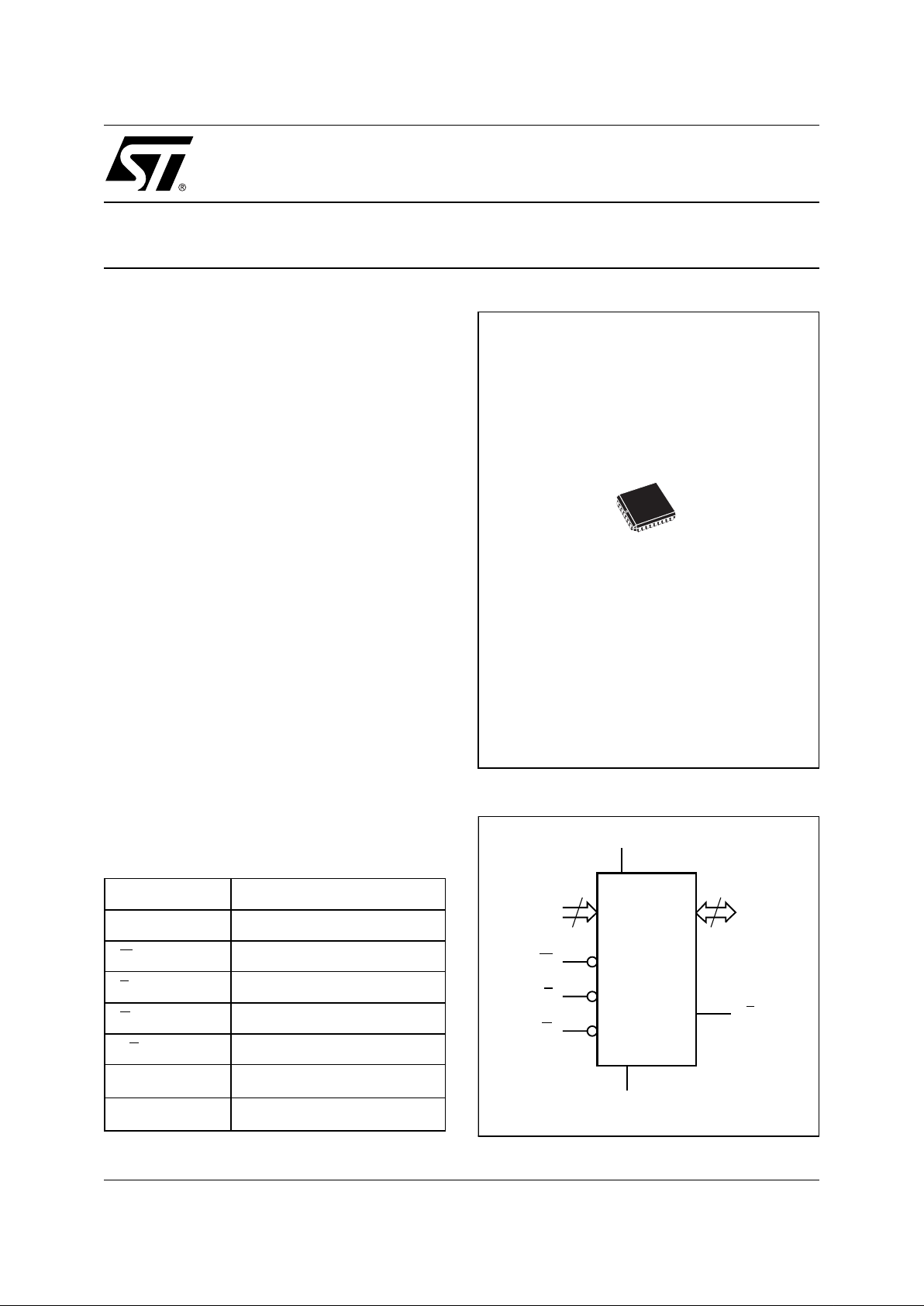
PLCC32 (K)
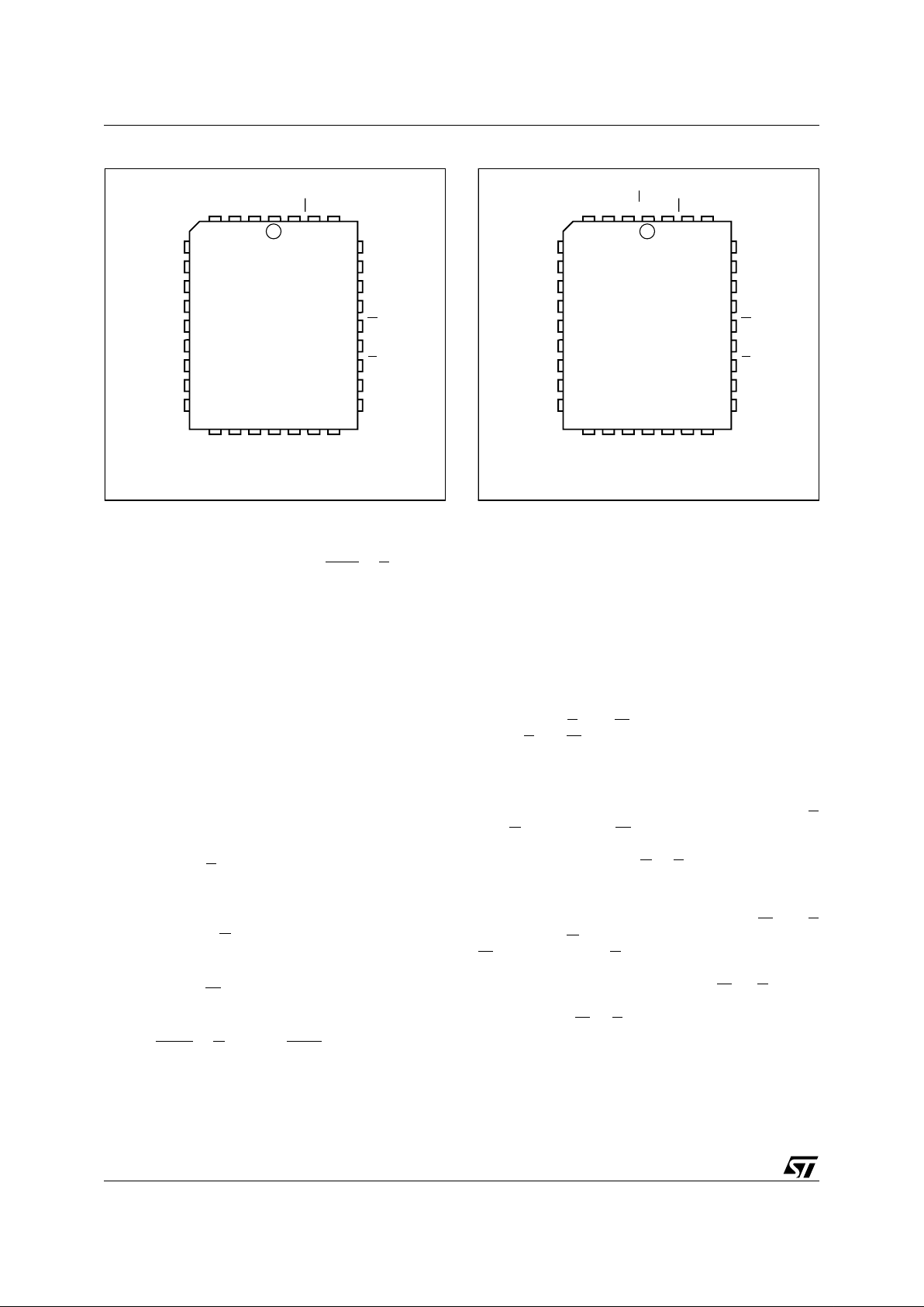
M28C16B, M28C17B
2/17
Figure 2A. PLLC Connections
Note: 1. NC = Not Connected
AI02817
NC
A8
A10
DQ4
17
A0
NC
DQ0
DQ1
DQ2NCDQ3
A6
A3
A2
A1
A5
A4
9
W
A9
1
NC
NC
DQ6
A7
DQ7
32
NC
V
CC
M28C16B
NC
NC
DQ5
G
E
25
V
SS
Figure 2B. PLLC Connections
Note: 1. NC = Not Connected
AI02830
NC
A8
A10
DQ4
17
A0
NC
DQ0
DQ1
DQ2NCDQ3
A6
A3
A2
A1
A5
A4
9
W
A9
1
NC
NC
DQ6
A7
DQ7
32
RB
V
CC
M28C17B
NC
NC
DQ5
G
E
25
V
SS
The M28C17B is like the M28C16B in every way,
except that it has an extra ready/busy
(RB) output.
The device has been designed to offer a flexible
microcontroller interface, featuring software handshaking, with Data Polling and Toggle Bit. The device supports a 64 byte Page Write operation.
Software Data Protection (SDP) is also supported,
using the standard JEDEC algorithm.
SIGNAL DESCRIPTION
The external connections to the device are summarized in Table 1, and their use in Table 3.
Addresses (A0-A10). The address inputs are
used to select one byte from the memory array
during a read or write operation.
Data In/Out (DQ0-DQ7). The contents of the data
byte are written to, or read from, the memory array
through the Data I/O pins.
Chip Enable (E
). The chip enable input must be
held low to enable read and write operations.
When Chip Enable is high, p ower consumpti on is
reduced.
Output Enable (G
). The Output Enable input con-
trols the data output buffers, and is used to initiate
read operations.
Write Enable (W
). The Write Enable input controls
whether the addressed location is to be read, from
or written to.
Ready/Busy
(RB). Ready/Busy (on the M28C17B
only) is an open drain output that can be us ed to
detect the end of the internal write cycle.
DEVICE OPERATION
In order to prevent data corruption and inadvertent
write operations, an internal V
CC
comparator in-
hibits the Write operations if the V
CC
voltage is
lower than V
WI
(see Table 4A). Once the voltage
applied on the V
CC
pin goes over the VWI thresh-
old (V
CC>VWI
), write access to the memory is al-
lowed after a time-out t
PUW
, as specified in Table
4A.
Further protection against data corruption is of-
fered by the E
and W low pass filters: any glitch,
on the E
and W inputs, with a pulse width less than
10 ns (typical) is inte rnally filtered out to prevent
inadvertent write operations to the memory.
Read
The device is accessed like a static RAM. When E
and G are low, and W is high, the contents of the
addressed location are presented on the I/ O pi ns.
Otherwise, when either G
or E is high, the I/O pins
revert to their high impedance state.
Write
Write operations are initiated when both W
and E
are low and G i s high. The device supports both
W
-controlled and E-controlled write cycles (as
shown in Figure 11 and Figure 12). The address is
latched during the falling edge of W
or E (which
ever occurs later) and the data is latche d on the
rising edge of W
or E (which ever occurs first). Af-
ter a delay, t
WLQ5H
, that cannot be shorter than the
value specified in Table 10A, the internal write cycle starts. It continues, under internal timing control, until the write operation is complete. The
commencement of this period can be det ecte d by
reading the Page Load Timer Status on DQ5. The
3/17
M28C16B, M28C17B
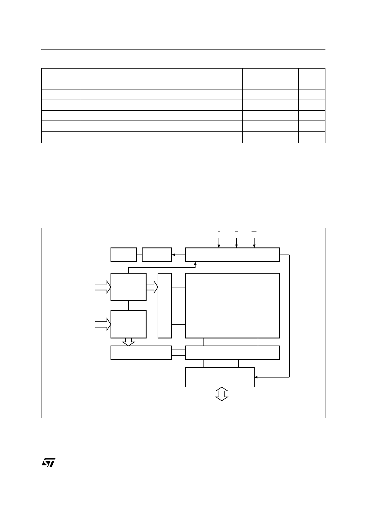
Figure 3. Block Diagram
AI02818
ADDRESS
LATCH
A6-A10
(Page Address)
X DECODE
CONTROL LOGIC
16K ARRAY
ADDRESS
LATCH
A0-A5
Y DECODE
VPP GEN RESET
SENSE AND DATA LATCH
I/O BUFFERS
EGW
PAGE LOAD
TIMER STATUS
TOGGLE BIT
DATA POLLING
DQ0-DQ7
Table 2. Absolute Maximum Ratings
1
Note: 1. Except for the rating “Operat i ng Temperature Ra nge”, stresses above those listed in t he Table “A bsolute Maximum Ratings” m ay
cause permanent damage to the device. These are stress ratings only, and operation of the device at these or any other conditions
above those indi cated in t he Operating sect i ons of thi s specifi cation i s not impl i ed. Exposure to Absolute M aximum Rating c onditions for extended periods may affect device reliability. Refer also to the ST SURE Program and other relevant quality documents.
2. MIL-ST D-883C, 3015.7 (100 pF, 15 00 Ω)
Symbol Parameter Value Unit
T
A
Ambient Operating Temperature -40 to 125 °C
T
STG
Storage Temperature -65 to 150 °C
V
CC
Supply Voltage -0.3 to 6.5 V
V
IO
Input or Output Voltage
-0.6 to V
CC
+0.6
V
V
I
Input Voltage -0.3 to 6.5 V
V
ESD Electrostatic Discharge Voltage (Human Body model)
2
4000 V
M28C16B, M28C17B
4/17
Table 3. Operating Modes
1
Note: 1. 0=VIL; 1=VIH; X = V
IH
or V
IL
; V=12V ± 5%.
Mode E G W DQ0-DQ7
Stand-by 1 X X Hi-Z
Output Disable X 1 X Hi-Z
Write Disable X X 1 Hi-Z
Read 0 0 1 Data Out
Write 0 1 0 Data In
Chip Erase 0 V 0 Hi-Z
end of the cycle can be detected by reading the
status of the Data Polling and the Toggle Bit functions on DQ7 and DQ6.
Page Write
The Page Write mode allows u p to 64 by tes to be
written on a single page in a single go. This is
achieved through a series of successive Write operations, no two of which are separated by more
than the t
WLQ5H
value (as specified in Table 10A).
The page write can be initiated during any byte
write operation. Following the first byte write instruction the host may send another address and
data with a minimum data transfer rate of:
1/t
WLQ5H
.
The internal write cycle can start at any instant after t
WLQ5H
. Once initiated, the write operation is internally timed, and continues, uninterrupt ed, until
completion.
All bytes must be located on the same page address (A10-A6 must be the same for all bytes).
Otherwise, the Page Write operation is not executed.
As with the single byte Write operation, described
above, the DQ5, DQ6 and DQ7 lines can be used
to detect the beginning and end of the internally
controlled phase of the Page Write cycle.
Software Data Protection (SDP)
The device offers a software-controlled write-protection mechanism that allows the user to inhibit all
write operations to the device. This c an be usef ul
for protecting the memory f rom inadvertent write
cycles that may occur during periods of instability
(uncontrolled bus conditions when excessive
noise is detected, or when power supply levels are
outside their specified values).
By default, the device is shipped in the “unprotected” state: the memory contents can be freely
changed by the user. Once the Software Data Protection Mode is enabled, all write com mands are
Table 4A. Power-Up Timing
1
for M28CxxB (5V range)
(T
A
= 0 to 70 °C or -40 to 85 °C; VCC = 4.5 to 5.5 V)
Note: 1. Sampled only, not 100% tested.
Table 4B. Power-Up Timing1 for M28CxxB-W (3V range)
(T
A
= 0 to 70 °C or -40 to 85 °C; VCC = 2.7 to 3.6 V)
Note: 1. Sampled only, not 100% tested.
Symbol Parameter Min. Max. Unit
t
PUR
Time Delay to Read Operation 1 µs
t
PUW
Time Delay to Write Operation (once VCC ≥ VWI)
10 ms
V
WI
Write Inhibit Threshold 3.0 4.2 V
Symbol Parameter Min. Max. Unit
t
PUR
Time Delay to Read Operation 1 µs
t
PUW
Time Delay to Write Operation (once VCC ≥ VWI)15ms
V
WI
Write Inhibit Threshold 1.5 2.5 V
5/17
M28C16B, M28C17B
ignored, and have no effect on the memory contents .
The device remains in this mode until a valid Software Data Protection disable sequence is re-
ceived. The device reverts to its “unprotected”
state.
The status of the Software Data Protection (enabled or disabled) is represented by a non-volatile
latch, and is remembered across periods of the
power being off.
The Software Data Protection Enable command
consists of the writing of three specific data bytes
to three specific memory locations (each location
being on a different page), as shown in Figure 4.
Similarly to disable the Software Data Protection,
the user has to write specific data bytes into six dif-
ferent locations, as shown in Figure 6. This complex series of operations protects against the
chance of inadvertent enabling or disabling of the
Software Data Protection mechanism.
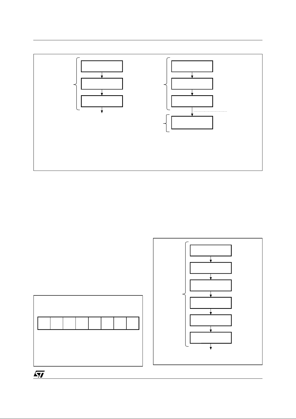
Figure 4. Software Data Protection Enable Algorithm and Memory Write
Note: 1. The most sign i ficant addre ss bits (A1 0 to A6) differ during the se specific Page Write operations.
AI02819
Write AAh in
Address 555h
Write 55h in
Address 2AAh
Write A0h in
Address 555h
SDP is set
Write AAh in
Address 555h
Write 55h in
Address 2AAh
Write A0h in
Address 555h
Page Write
(1 up to 64 bytes)
Write to Memory
When SDP is SET
SDP Enable Algorithm
Page Write
Timing
(see note 1)
Page Write
Timing
(see note 1)
Write
is Enabled
Physical
Page Write
Instruction
Figure 5. Sta tu s B it As si gnment
AI02815
DP TB PLTS Hi-Z Hi-Z Hi-Z Hi-Z Hi-Z
DP
TB
PLTS
Hi-Z
DQ7 DQ6 DQ5 DQ4 DQ3 DQ2 DQ1 DQ0
= Data Polling
= Toggle Bit
= Page Load Timer Status
= High impedance
Figure 6. Software Data Protection Disable
Algorithm
AI02820
Write AAh in
Address 555h
Write 55h in
Address 2AAh
Write 80h in
Address 555h
Unprotected State
Write AAh in
Address 555h
Write 55h in
Address 2AAh
Write 20h in
Address 555h
Page Write
Timing
M28C16B, M28C17B
6/17
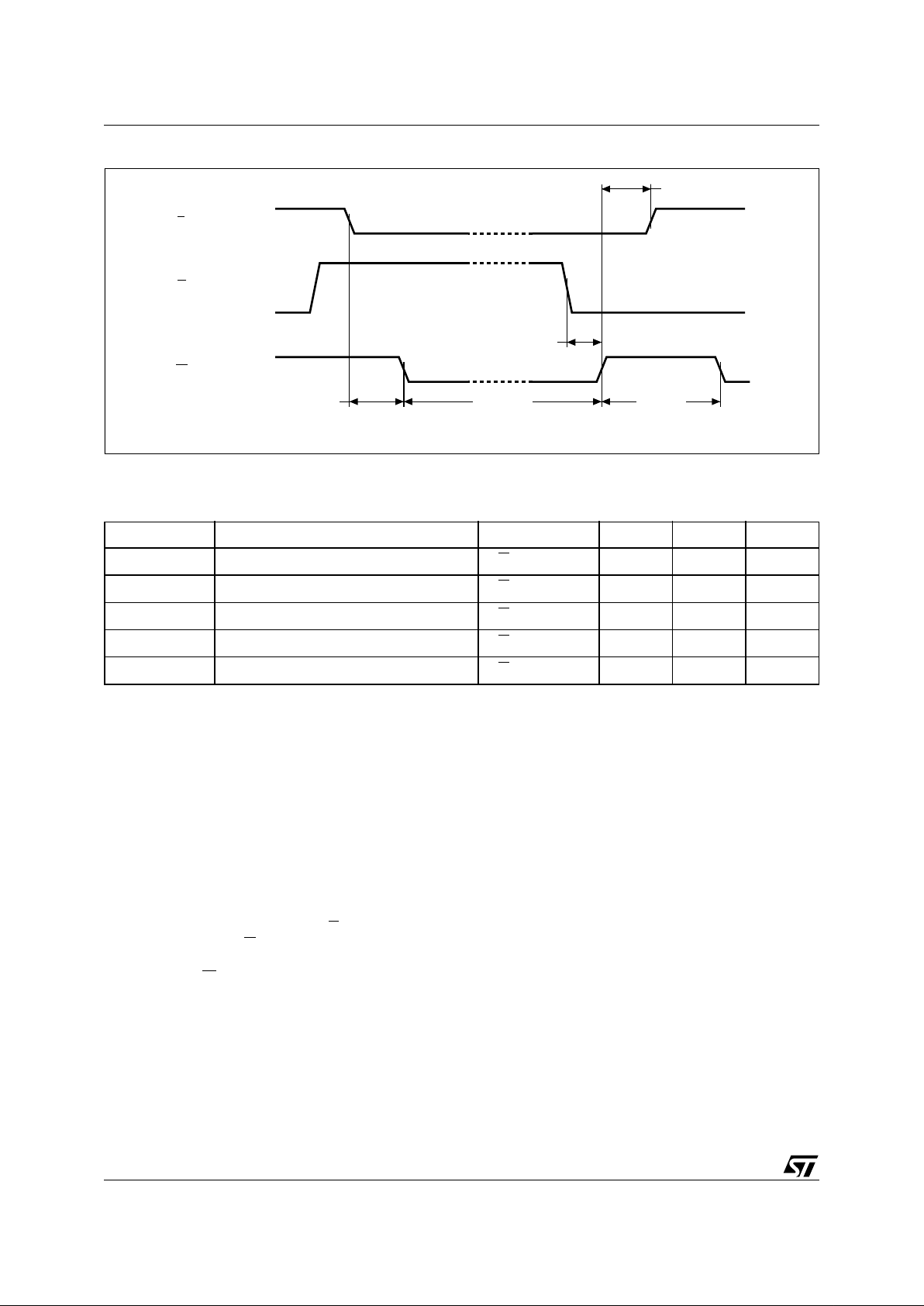
Table 5. Chip Erase AC Characteristics
1
(TA = 0 to 70 °C or -40 to 85 °C; VCC = 4.5 to 5.5 V or 2.7 to 3.6 V)
Note: 1. Sampled only, not 100% tested.
Symbol Parameter Test Condition Min. Max. Unit
t
ELWL
Chip Enable Low to Write Enable Low
G
= VCC + 7V
1 µs
t
WHEH
Write Enable High to Chip Enable High G = VCC + 7V 0 ns
t
WLWH2
Write Enable Low to Write Enable High G = VCC + 7V 10 ms
t
GLWH
Output Enable Low to Write Enable High
G
= VCC + 7V
1µs
t
WHRH
Write Enable High to Write Enable Low G = VCC + 7V 3 ms
Figure 7. Chip Erase AC Waveforms
AI01484B
E
G
W
tWLWH2tELWL
tGLWH
tWHRH
tWHEH
When SDP is enabled, the memory array can still
have data written to it, but the sequence is more
complex (and hence better protected from inadvertent use). The seque nce is as shown in Figure
4. This consists of an unlock key, to enable the
write action, at the end of which the SDP continues
to be enabled. This allows the SDP to be enabled,
and data to be written, within a single Write cycle
(t
WC
).
Software Chip Erase
The contents of the entire memory are erased ( set
to FFh) by holding Chip Enable (E
) low, and hold-
ing Output Enable (G
) at VCC+7.0V. The chip is
cleared when a 10 ms low pulse is applied to the
Write Enable (W
) signal (see Figure 7 and Table 5
for details).
Status Bits
The devices provide three status bits (DQ7, DQ6
and DQ5), for use d uring write operation s. These
allow the application to use t he write time la tency
of the device for getting on with other work. These
signals are available on the I/O port bits DQ7, DQ6
and DQ5 (but only during programming cycle,
once a byte or more has been latched into the
memory).
Data Polling bit (DQ7). The internally timed write
cycle starts after t
WLQ5H
(defined in Table 10A)
has elapsed since the previous byte was latched in
to the memory. The value of the DQ7 bit of this last
byte, is used as a signal throughout this write operation: it is inverted while the internal write operation is underway, and is inverted back to its
original value once the operation is complete.
Toggle bit (DQ6). The device offers another way
for determining when the internal write cycle is
completed. During the internal E rase/Write cycle,
DQ6 toggles from ’0’ to ’1’ and ’1’ to ’0’ (the first
read value being ’0’) on subsequent att empts to
read any byte of the memory. When the internal
write cycle is complete, the toggling is stopped,
and the values read on DQ7-DQ0 are those of the
addressed memory byte. This indicates that the
device is again avai lable for new Read and Write
operations.
Page Load Timer Status bit (DQ5). An internal
timer is used to measure the period bet ween suc -
 Loading...