

M28C16A
M28C17A
16 Kbit (2Kb x8) Parallel EEPROM
August 1998 1/19
AI02109
11
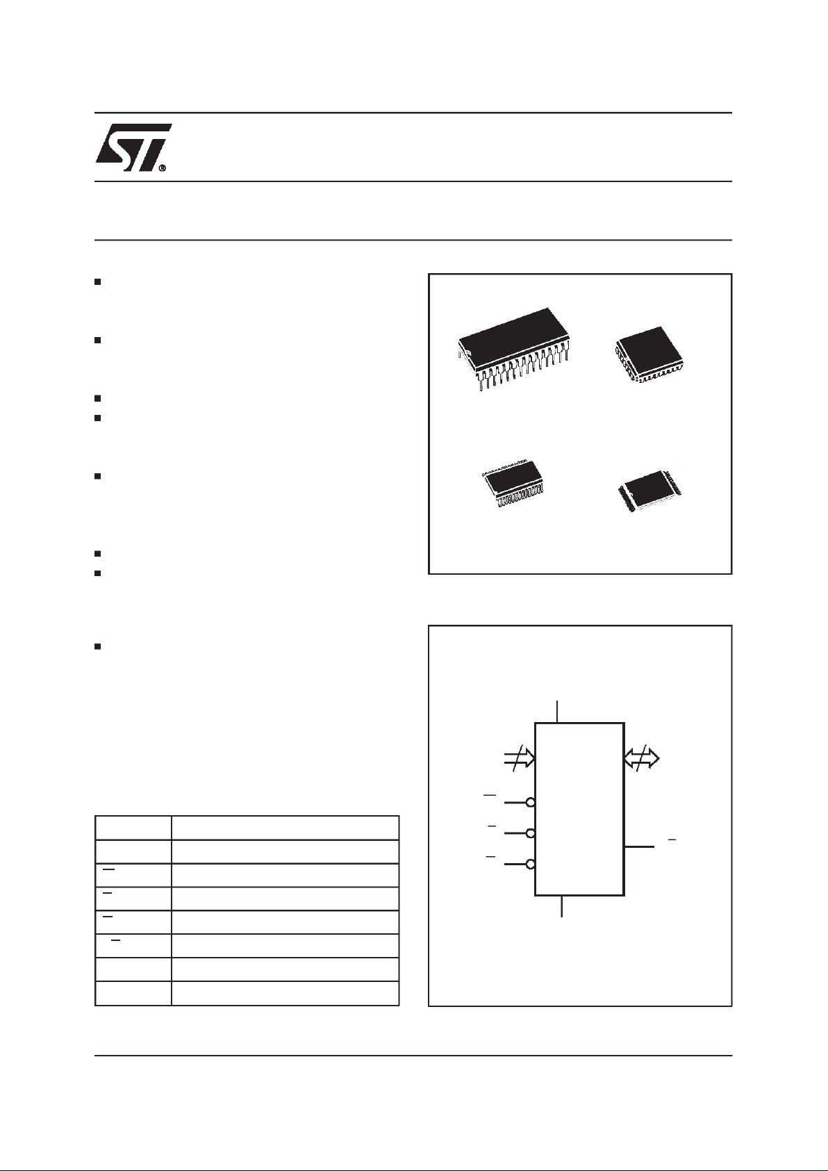
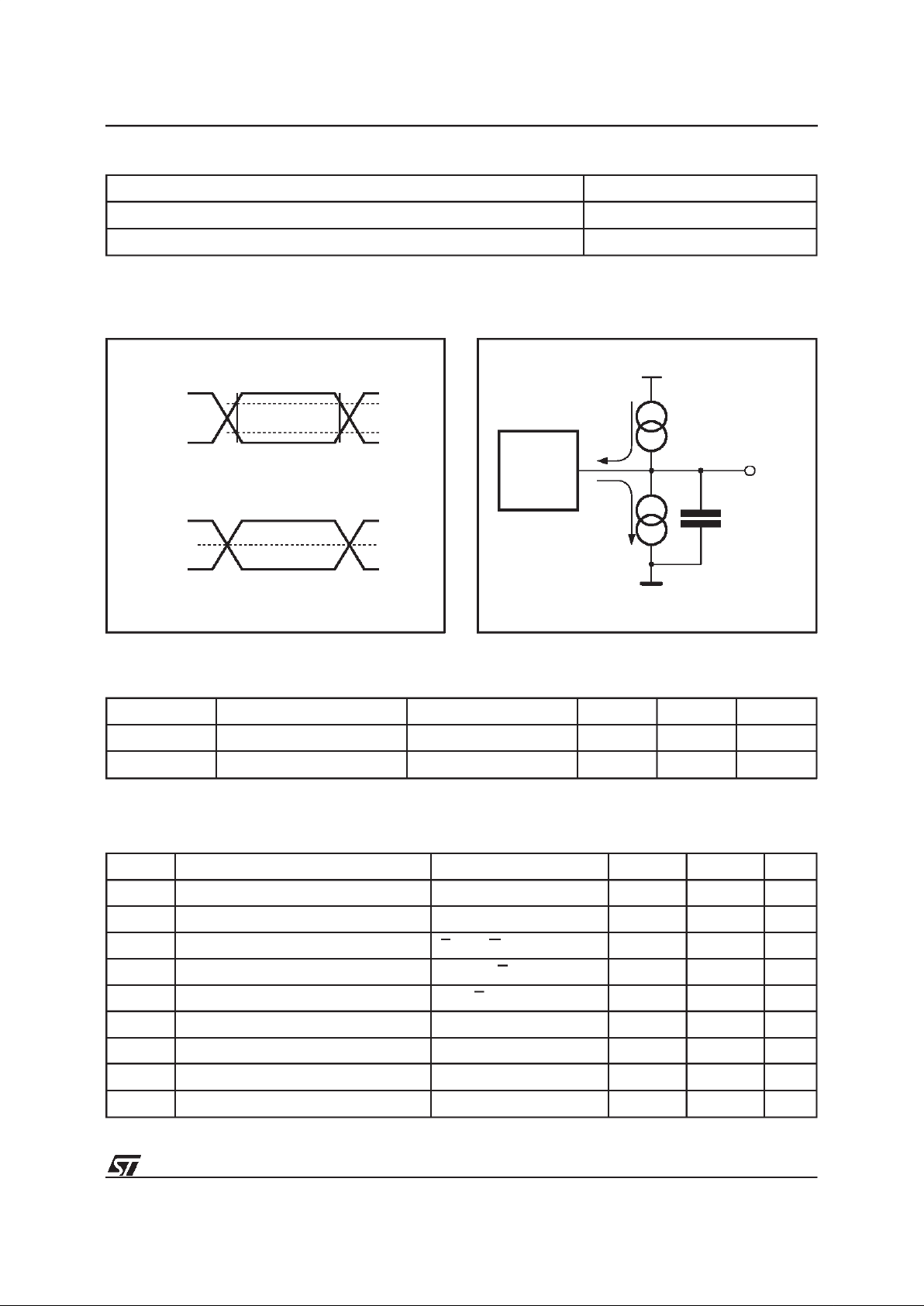
A0-A10
W
DQ0-DQ7
V
CC
M28C16A
M28C17A
G
E
V
SS
8
RB
Figure1. Logic Diagram
28
1
PDIP28 (BS) PLCC32 (KA)
A0-A10 Address Input
DQ0-DQ7 Data Input / Output
W Write Enable
E Chip Enable
G Output Enable
RB Ready / Busy
V
CC
Supply Voltage
V
SS
Ground
Table1. SignalNames
FASTACCESSTIME:
– 150ns at 5V
– 250ns at 3V
SINGLE SUPPLYVOLTAGE:
–5V±10%forM28C16Aand M28C17A
– 2.7V to 3.6VforM28C16-xxW
LOW POWERCONSUMPTION
FASTWRITE CYCLE
– 32 BytesPage Write Operation
– Byte or Page Write Cycle: 5ms
ENHANCEDENDOF WRITEDETECTION
– Ready/BusyOpenDrainOutput
– Data Polling
– ToggleBit
PAGELOAD TIMERSTATUSBIT
HIGH RELIABILITYSINGLE POLYSILICON,
CMOSTECHNOLOGY
– Endurance>100,000Erase/WriteCycles
– Data Retention >40 Years
JEDECAPPROVED BYTEWIDEPIN OUT
DESCRIPTION
TheM28C16Aand M28C17Aare 2Kx8 low power
ParallelEEPROMfabricatedwithSTMicroelectronicsproprietarysinglepolysiliconCMOStechnology.
The device offers fast access time withlow power
dissipationand requiresa 5V or3V powersupply.
TSOP28 (NS)
8 x13.4mm
28
1
SO28 (MS)
300 mils
A1
A0
DQ0
A7
A4
A3
A2
A6
A5
DU
A10
A8
A9
DQ7
W
NC
G
E
DQ5DQ1
DQ2
DQ3V
SS
DQ4
DQ6
NC
RB V
CC
AI02110
M28C17A
8
1
2
3
4
5
6
7
9
10
11
12
13
14
16
15
28
27
26
25
24
23
22
21
20
19
18
17
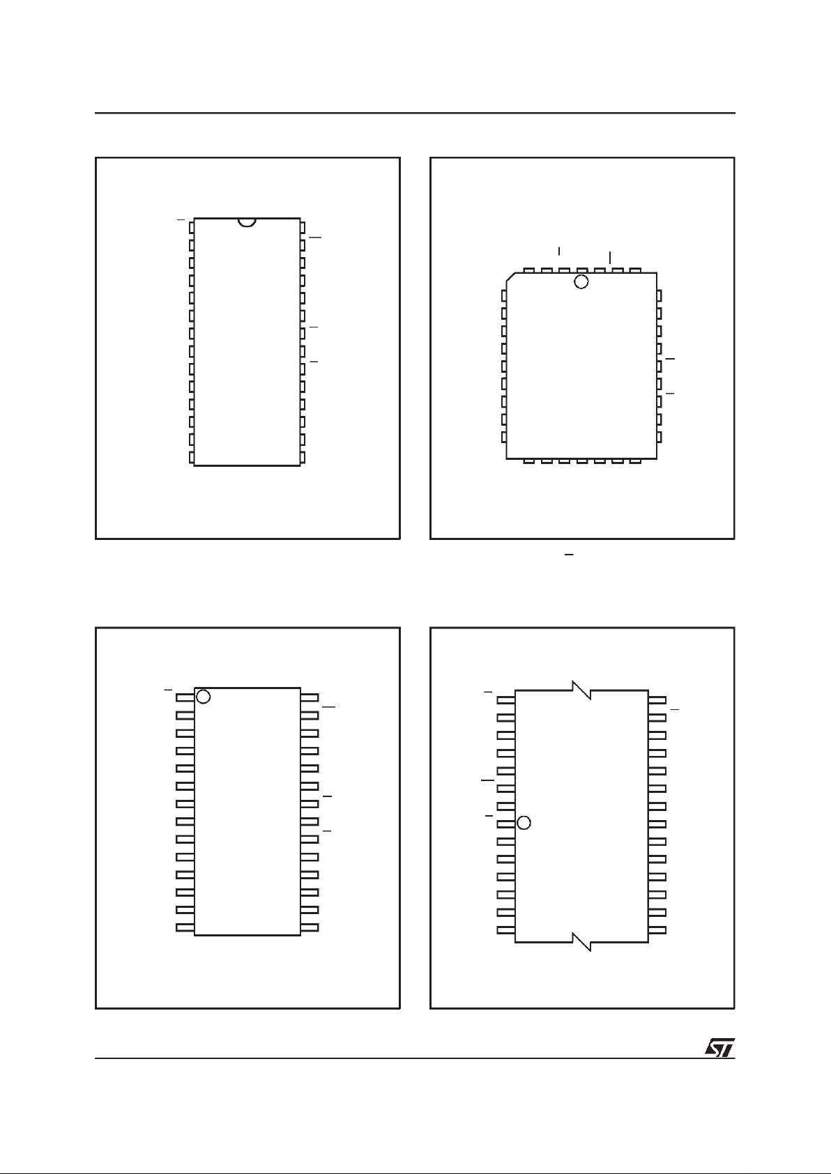
Figure2A. DIP Pin Connections
Warning: NC = Not Connected, DU = Don’t Use.
AI02111
DU
A8
A10
DQ4
17
A0
NC
DQ0
DQ1
DQ2NCDQ3
A6
A3
A2
A1
A5
A4
9
W
A9
1
RB or NC
(1)
NC
DQ6
A7
DQ7
32
DU
V
CC
M28C16A
M28C17A
NC
NC
DQ5
G
E
25
V
SS
Figure2B. LCC Pin Connections
Warning: NC = Not Connected, DU = Don’t Use.
Note:
1. Pin 2 is either RB for M28C17Aor NC
for M28C16A.
A1
A0
DQ0
A5
A2
A4
A3
A9
NC
DQ7
A8
G
E
DQ5
DQ1
DQ2
DQ3
DQ4
DQ6
DU
W
NC
A6
RB
V
CC
A7
AI02113
M28C16A
28
1
22
78
14
15
21
V
SS
A10
Figure2D. TSOP Pin Connections
Warning: NC = Not Connected, DU = Don’t Use.
DQ0
DQ1
A3
A0
A2
A1
A10
E
DU
DQ7
G
DQ5
V
CC
DQ4
A9
W
A4
RB
A7
AI02112
M28C17A
8
2
3
4
5
6
7
9
10
11
12
13
14
22
21
20
19
18
17
16
15
DQ2
V
SS
A6
A5
DQ6
28
27
26
25
24
23 NC
DQ3
1
NC
A8
Figure2C. SO Pin Connections
Warning: NC = Not Connected, DU = Don’t Use.
2/19
M28C16A, M28C17A
Symbol Parameter Value Unit
T
A
Ambient Operating Temperature
(2)
–40to85 °C
T
STG
Storage TemperatureRange – 65 to 150
°
C
V
CC
Supply Voltage – 0.3 to 6.5 V
V
IO
Input/Output Voltage – 0.3 to VCC+0.6 V
V
I
Input Voltage – 0.3 to 6.5 V
V
ESD
Electrostatic Discharge Voltage (Human Body model) 3000 V
Notes:
1. Except for therating ”Operating Temperature Range”, stressesabove thoselistedin theTable ”AbsoluteMaximum Ratings”
may cause permanentdamage to thedevice. Theseare stress ratingsonly and operationof the deviceat these or any other
conditions above those indicated inthe Operatingsections of this specification is not implied. Exposure to Absolute Maximum
Rating conditions for extendedperiods may affectdevice reliability.Refer also tothe STMicroelectronics SURE Programand other
relevant qualitydocuments.
2. Depends on range.
Table2. AbsoluteMaximum Ratings
(1)
Mode E G W DQ0 - DQ7
Read V
IL
V
IL
V
IH
Data Out
Write V
IL
V
IH
V
IL
Data In
Standby / Write Inhibit V
IH
X X Hi-Z
Write Inhibit X X V
IH
Data Out or Hi-Z
Write Inhibit X V
IL
X Data Out or Hi-Z
Output Disable X V
IH
X Hi-Z
Note:
X=V
IH
or V
IL
Table3. OperatingModes
The circuit has been designed to offer a flexible
microcontroller interface featuring both hardware
andsoftwarehandshakingmode withReady/Busy,
Data Polling and Toggle Bit. The M28C16A/17A
supports32 bytepage write operation.
PIN DESCRITPION
Addresses (A0-A10).
The address inputs select
an 8-bit memory location during a read or write
operation.
Chip Enable (E).
The chip enable input must be
lowtoenableall read/writeoperations.WhenChip
Enableishigh,power consumptionis reduced.
OutputEnable (G).
The OutputEnableinput controls the data output buffersand is used to initiate
readoperations.
DataIn/Out(DQ0-DQ7).
Datais writtentoorread
fromthe M28C16A/17Athroughthe I/O pins.
WriteEnable(W).
TheWriteEnableinputcontrols
the writingof data to the M28C16A/17A.
Ready/Busy (RB).
Ready/Busy is an open drain
output that can be used to detect the end of the
internalwritecycle.Ready/Busyisavailablefor the
M28C17Ain PDIP, PLCC and SO packages,and
for the M28C16Ain TSOPonly.
OPERATION
Inorderto preventdata corruptionand inadvertent
write operations during power-up, a Power On
Reset(POR)circuitresetsallinternalprogramming
cicuitry. Access to the memory in write mode is
allowedaftera power-upas specifiedin Table7.
Read
The M28C16A/17Ais accessedlike a staticRAM.
When E and G are low with W high, the data
addressed is presented on the I/O pins. The I/O
pinsarehighimpedancewheneitherGorEishigh.
DESCRIPTION
(cont’d)
3/19
M28C16A, M28C17A
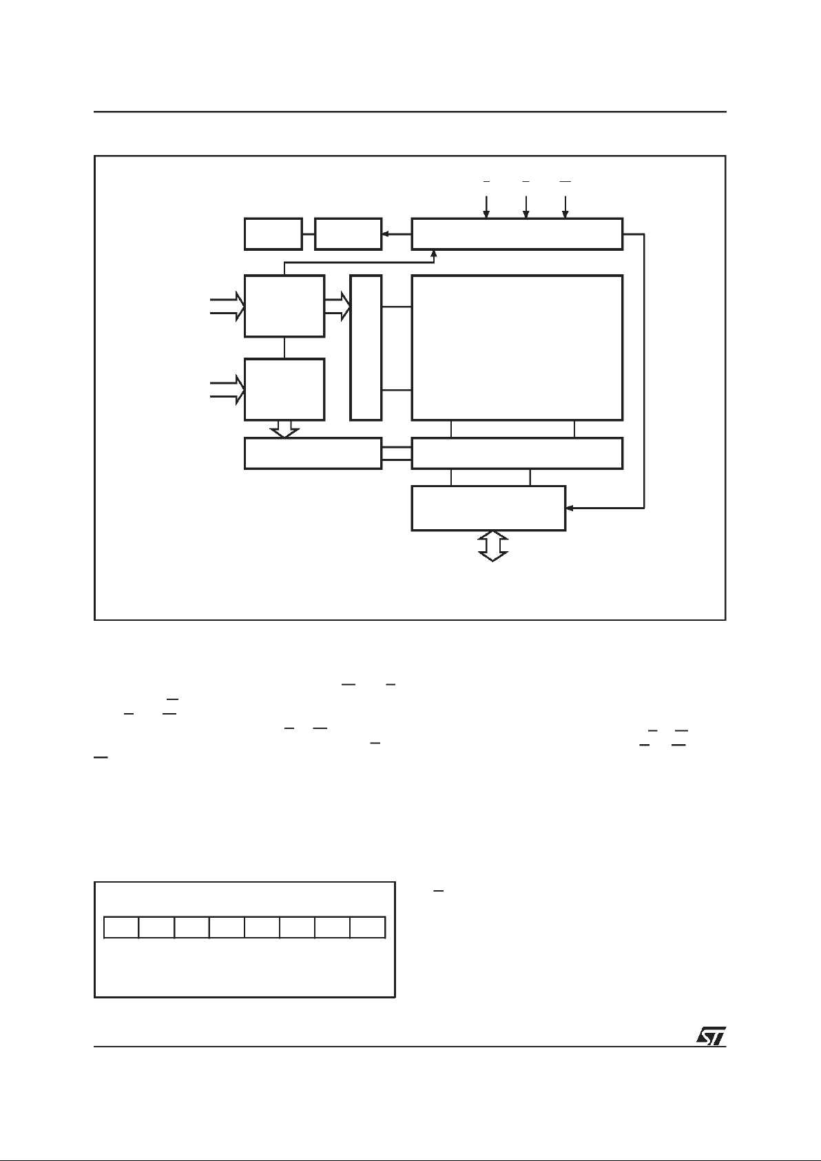
AI01520
ADDRESS
LATCH
A6-A10
(Page Address)
X DECODE
CONTROL LOGIC
64K ARRAY
ADDRESS
LATCH
A0-A5
Y DECODE
VPPGEN RESET
SENSE AND DATA LATCH
I/O BUFFERS
EGW
PAGE
LOAD
TIMER STATUS
TOGGLE BIT
DATA POLLING
DQ0-DQ7
Figure3. Block Diagram
Write
Write operations are initiatedwhen both W and E
arelowandG is high.TheM28C16A/17Asupports
bothEand W controlledwritecycles.The Address
is latchedbythefallingedge of E or W which ever
occurslast and the Data on therising edgeof Eor
W which ever occurs first.Once initiatedthe write
operationis internally timed until completion.
Page Write
Page write allows up to 32 bytes to be consecutively latched into the memory prior to initiating a
DQ7 DQ6 DQ5 DQ4 DQ3 DQ2 DQ1 DQ0
DP TB PLTS Hi-Z Hi-Z Hi-Z Hi-Z Hi-Z
Figure4. Status Bit Assignment
DP = Data Polling
TB = Toggle Bit
PLTS = Page Load TimerStatus
programming cycle.All bytes must be located in a
single pageaddress, that is A5- A10 must be the
samefor all bytes. The page write can be initiated
duringany bytewrite operation.
Following the first byte write instruction the host
may sendanotheraddress and data up to amaximumof t
WHWH
afterthe risingedge ofE orW which
ever occurs first. If a transition of E or W is not
detected within t
WHWH
, the internal programming
cyclewill start.
Microcontroller Control Interface
The M28C16A/17A provides two write operation
status bits and one status pin that can be used to
minimize thesystemwritecycle.These signalsare
available on the I/O port bits DQ7 or DQ6 of the
memoryduring programming cycle only, or as the
RB signalon a separate pin.
Data Polling bit (DQ7). During the internal write
cycle, any attempt to read the last byte written will
produce on DQ7 the complementaryvalue of the
previouslylatched bit. Once the write cycle is finished the true logic value appears on DQ7 in the
readcycle.
OPERATION(cont’d)
4/19
M28C16A, M28C17A
Symbol Parameter Test Condition Min Max Unit
C
IN
Input Capacitance VIN=0V 6 pF
C
OUT
Output Capacitance V
OUT
=0V 12 pF
Note:
1. Sampled only, not 100% tested.
Table5. Capacitance
(1)
(TA=25°C, f =1 MHz)
Symbol Parameter TestCondition Min Max Unit
I
LI
Input Leakage Current 0V ≤ VIN≤ V
CC
10 µA
I
LO
Output Leakage Current 0V ≤ VIN≤ V
CC
10 µA
I
CC
(1)
Supply Current (TTLand CMOS inputs) E = VIL,G=VIL, f = 5MHz 25 mA
I
CC1
(1)
Supply Current (Standby) TTL E = V
IH
1mA
I
CC2
(1)
Supply Current (Standby) CMOS E > VCC– 0.3V 50
µ
A
V
IL
Input Low Voltage –0.3 0.8 V
V
IH
Input High Voltage 2 VCC+ 0.5 V
V
OL
Output Low Voltage IOL= 2.1 mA 0.4 V
V
OH
Output High Voltage IOH= –400 µA 2.4 V
Note:
1. All I/O’sopen circuit.
Table6. Read ModeDC Characteristicsfor M28C16Aand M28C17A
(T
A
=–40 to 85°C, VCC= 4.5Vto5.5V)
Input Rise and Fall Times
≤
20ns
Input Pulse Voltages 0.4V to 2.4V
Input and Output TimingRef. Voltages 0.8V to 2.0V
Note thatOutput Hi-Z isdefined as the point wheredata is no longer driven.
Table4. AC MeasurementConditions
AI02101B
4.5V to 5.5V Operating Voltage
2.7V to 3.6V Operating Voltage
VCC– 0.3V
0V
0.5 V
CC
2.4V
0.4V
2.0V
0.8V
Figure5. AC TestingInput Output Waveforms
AI02114
OUT
CL= 30pF
CLincludes JIG capacitance
I
OL
DEVICE
UNDER
TEST
I
OH
V
CC
Figure6. AC TestingEquivalent LoadCircuit
5/19
M28C16A, M28C17A
Symbol Parameter Test Condition Min Max Unit
I
LI
Input Leakage Current 0V≤V
IN
≤
V
CC
10
µ
A
I
LO
Output Leakage Current 0V ≤ VIN≤ V
CC
10 µA
I
CC
(1)
Supply Current (TTLand CMOS inputs) E = VIL,G=VIL,f=5MHz 15 mA
I
CC2
(1)
Supply Current (Standby) CMOS E > VCC–0.3V 20 µA
V
IL
Input Low Voltage –0.3 0.6 V
V
IH
Input High Voltage 2 VCC+ 0.5 V
V
OL
Output Low Voltage IOL= 2.1 mA 0.2 V
CC
V
V
OH
Output High Voltage IOH= –400 µA 0.8 V
CC
V
Note: 1. All I/O’s open circuit.
Table8. Read ModeDC Characteristicsfor M28C16A-W
(T
A
=–40 to 85°C, VCC= 2.7Vto3.6V)
Symbol Parameter Min Max Unit
t
PUR
Time Delay to Read Operation 1
µ
s
t
PUW
Time Delay to Write Operation (once VCC≥ VWI)10ms
V
WI
Write InhibitThreshold 1.5 2.5 V
Note: 1. Sampled only,not 100% tested.
Table9. PowerUp Timingfor M28C16A-W
(1)
(TA= –40 to 85°C, VCC= 2.7V to 3.6V)
Symbol Parameter Min Max Unit
t
PUR
Time Delay to Read Operation 1 µs
t
PUW
Time Delay to Write Operation (once VCC≥ VWI)10ms
V
WI
Write InhibitThreshold 1.5 2.5 V
Note:
1. Sampled only, not 100% tested.
Table7. PowerUp Timingfor M28C16A andM28C17A
(1)
(T
A
=
–40 to 85°C, V
CC
= 4.5V to 5.5V)
6/19
M28C16A, M28C17A
 Loading...