

Low Voltage UV EPROM and OTP EPROM
■ 2.7 to 3.6V LOW VOLTAGE in READ
OPERATION
■ READ ACCESS TIME:
–80ns at V
– 100ns at V
■ BYTE-WIDE or WORD-WIDE
CONFIGURABLE
■ 4 Mbit MASK ROM REPLACEMENT
■ LOW POWER CONSUMPTION
– Active Current 20mA at 8MHz
– Stand-by Current 15µA
■ PROGRAMMI N G VOLT AG E: 1 2.5V ± 0.25V
■ PROGRAMMING TIME: 50µs/word
■ ELECTRONIC SIGNATURE
– Manufacturer Code: 20h
– Device Code: B8h
DESCRIPTION
The M27W400 is a low voltage 4 Mbit EPROM offered in the two range UV (Ultra Violet Erase) and
OTP (one time programmab le). It is ideally suited
for microprocessor systems requiring large data or
program storage. It is organised as either 512
Kwords of 8 bit or 256 Kwords of 16 bit. The pinout is compatible with the most common 4 Mbit
Mask ROM.
The M27W400 operates in the read mode with a
supply voltage as low as 2.7V at –40 to 85°C temperature range. The decrease in operating power
allows either a reduction of the size of the battery
or an increase in the time between battery recharges.
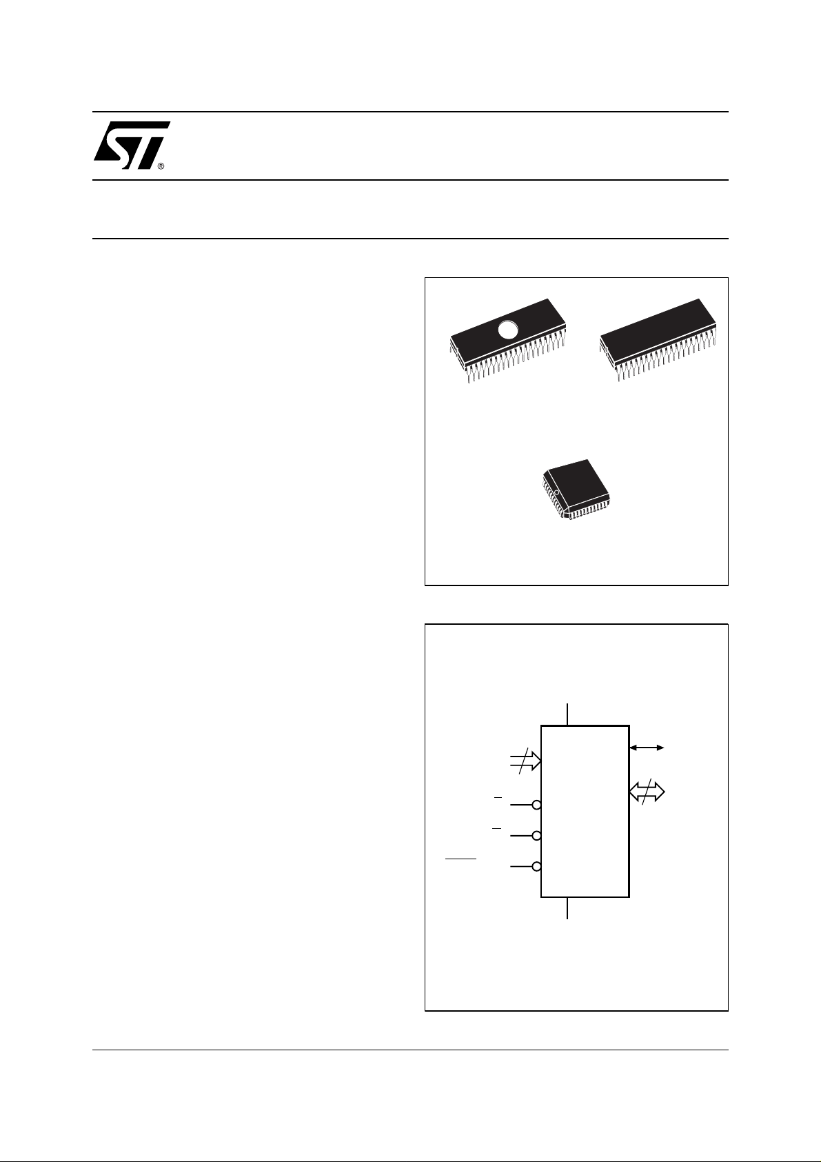
The FDIP40W (window ceramic frit-seal package)
has a transparent lid which all ows the user to expose the chip to ultraviolet light to erase the bit pattern. A new pattern can then be written to the
device by following the programming procedure.
For application where the content is programmed
only one time and erasure is not required, the
M27W400 is offered in PDIP40 and PLCC44 packages.
= 3.0 to 3.6V
CC
= 2.7 to 3.6V
CC
M27W400
4 Mbit (512Kb x8 or 256Kb x16)
40
1
FDIP40W (F) PDIP40 (B)
PLCC44 (K)
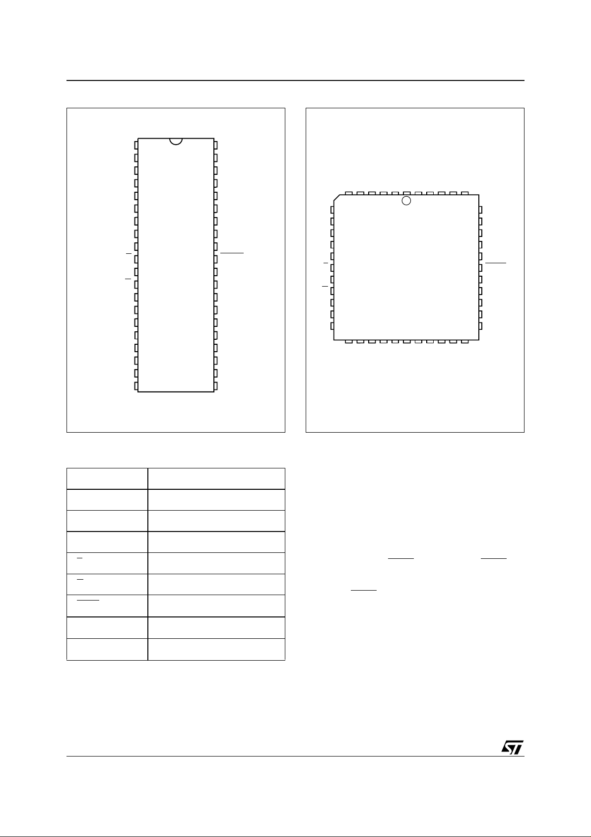
Figure 1. Logic Diagram
18
A0-A17
E
G
BYTEV
PP
40
V
CC
M27W400
V
SS
1
Q15A–1
15
Q0-Q14
AI03096
1/15January 2000
M27W400
Figure 2A. DIP Connections
A17 A8
1
2
A7
A6
3
4
A5
5
A4
A3
6
7
A2
A1
8
9
A0
E
10
M27W400
11
V
SS
G
12
13
Q0
14
Q8
15
Q1
16
Q9
17
Q2
18
19
Q3
Q11
40
39
38
37
36
35
34
33
32
31
30
29
28
27
26
25
24
23
22
2120
AI03097
A9
A10
A11
A12
A13
A14
A15
A16
BYTEV
V
SS
Q15A–1
Q7
Q14
Q6
Q13
Q5
Q12Q10
Q4
V
CC
PP
Figure 2B. LCC Connections
A7
A5
A6
A4
A3
A2
A1 A15
A0
E
12
V
SS
Q0
Q8
Q1
Q9
Q2
A17
M27W400
Q3
Q10
NC
1
23
Q11
NC
NC
44
NC
CC
V
A8
Q4
A9
Q12
A10
Q5
A11
34
Q13
A12
A13
A14
A16
BYTEV
V
SS
Q15A–1G
Q7
Q14
Q6
AI03604
PP
Table 1. Signal Names
A0-A17 Address Inputs
Q0-Q7 Data Outputs
Q8-Q14 Data Outputs
Q15A–1 Data Output / Address Input
E
G
BYTE
V
CC
V
SS
V
PP
Chip Enable
Output Enable
Byte Mode / Program Supply
Supply Voltage
Ground
DEVICE OPERATION
The operating modes of the M27W400 are listed in
the Operating Modes Table. A single power supply
is required in the read mode. All inputs are TTL
compatib le exc ept for V
and 12V on A9 for the
PP
Electronic Signature.
Read Mode
The M27W400 has two organisations, Wo rd-wide
and Byte-wide. The organisation is selected by the
signal level on the BYTE
VPP pin. When BYTEV
PP
is at VIH the Word-wide organisation is selected
and the Q15A–1 pin is used for Q15 Data Output.
When the BYTE
VPP pin is at VIL the Byte-wide organisation is selected and the Q15A–1 pin is used
for the Address Input A–1. When the memory is
logically regarded as 16 bit wid e, but read in the
Byte-wide organisation, then with A–1 at V
IL
the
lower 8 bits of the 16 bit data are selected and with
A–1 at V
the upper 8 bits of the 16 bit dat a are
IH
sele cte d.
2/15
M27W400
Table 2. Absolute Maximum Ratings
(1)
Symbol Parameter Value Unit
T
A
T
BIAS
T
STG
(2)
V
IO
V
CC
(2)
V
A9
V
PP
Note: 1. Except for the rating “Operating Temperature Range”, s tr esses above those li sted in t he Table “Absolute M aximum Rat i ngs” may
cause permanent damage to the device. These are stress ratings only and operation of the device at these or any other conditions
above those indi cated in t he Operat ing sections of thi s specif i cation is not impl i ed. Exposure to Absolute Maximum Rating conditions for extended per iods may aff ect device reliabilit y. Refer also to the STMicroel ectronics SURE Program an d other relevan t qual ity docum en ts .
2. Minim um DC vo ltage on Inpu t or Out put is – 0.5V w ith po ssible undersh oot to –2.0V fo r a pe riod les s than 20ns. Ma ximu m DC
voltage on Output is V
3. Depends on range.
Ambient Operating Temperature
Temperature Under Bias –50 to 125 °C
Storage Temperature –65 to 150 °C
Input or Output Voltage (except A9) –2 to 7 V
Supply Voltage –2 to 7 V
A9 Voltage –2 to 13.5 V
Program Supply Voltage –2 to 14 V
+0.5V with possible overshoot to VCC +2V for a period l ess than 20ns.
CC
(3)
–40 to 125 °C
Table 3. Operating Modes
Mode E
Read Word-wide
Read Byte-wide Upper
Read Byte-wide Lower
Output Disable
Program
V
IL
Verify
Program Inhibit
Standby
Electronic Signature
Note: X = VIH or VIL, VID = 12V ± 0.5V.
V
IL
V
IL
V
IL
V
IL
Pulse V
V
IH
V
IH
V
IH
V
IL
V
V
V
V
V
V
V
BYTEV
G
IL
IL
IL
IH
IH
IL
IH
V
IH
V
IL
V
IL
X X Hi-Z Hi-Z Hi-Z
V
PP
V
PP
V
PP
A9 Q7-Q0 Q14-Q8 Q15A–1
PP
X Data Out Data Out Data Out
X Data Out Hi-Z
X Data Out Hi-Z
X Data In Data In Data In
X Data Out Data Out Data Out
X Hi-Z Hi-Z Hi-Z
V
IH
V
IL
X X X Hi-Z Hi-Z Hi-Z
IL
V
IH
V
ID
Codes Codes Code
Table 4. Electronic Signature
Identifier A0
Manufacturer’s Code
Device Code
V
IL
V
IH
Q15
or Q7
Q14
or Q6
Q13
or Q5
Q12
or Q4
Q11
or Q3
Q10
or Q2
Q9 or Q1Q8 or
Q0
Hex Data
00100000 20h
10111000 B8h
3/15
M27W400
Table 5. AC Measurement Conditions
High Speed Standard
Input Rise and Fall Times ≤ 10ns ≤ 20ns
Input Pulse Voltages 0 to 3V 0.4V to 2.4V
Input and Output Timing Ref. Voltages 1.5V 0.8V and 2V
Figure 3. Tes ting Inp ut Output Wav ef orm
High Speed
3V
1.5V
0V
Standard
2.4V
0.4V
Table 6. Capacitance
Symbol Parameter Test Condition Min Max Unit
C
IN
C
OUT
Note: 1. Sampled only, not 100% tested.
Input Capacitance (except BYTEVPP)V
Input Capacitance (BYTE
Output Capacitance
(1)
(TA = 25 °C, f = 1 MHz)
2.0V
0.8V
AI01822
VPP)V
Figure 4. AC Testing Load Circuit
1.3V
1N914
3.3kΩ
DEVICE
UNDER
TEST
CL
CL = 30pF for High Speed
CL = 100pF for Standard
CL includes JIG capacitance
V
IN
IN
OUT
= 0V
= 0V
= 0V
10 pF
120 pF
12 pF
OUT
AI01823B
The M27W400 has two control functions, both of
which must be logically ac tive in order to obtain
data at the outputs. In addition the Word-wide or
Byte- wide organisation must be selected.
Chip Enable (E
used for device selection. Output Enable (G
) is the power control and should be
) is the
output control and should be used to gate data to
the output pins in dependent of device selection.
Assuming that the addresses are s table, the address access time (t
4/15
) is equal to the delay
AVQV
from E to output (t
output after a delay of t
, assuming that E has been low and the ad-
of G
dresses have been stable for at least t
). Data is available at the
ELQV
from the falling e dge
GLQV
AVQV-tGLQV
Standby Mode
The M27W400 has a standby mode which reduc-
es the supply current from 20mA to 15µA. The
M27W400 is placed in the standby mode by applying a CMOS high signal to the E
input. When in the
standby mode, the outputs are in a high impedance state, independent of the G
input.
.
M27W400
Table 7. Read Mode DC Characteristics
(1)
(TA = 0 to 70 °C or –40 to 85 °C; VCC = 2.7 to 3.6V; VPP = VCC)
Symbol Parameter Test Condition Min Max Unit
I
I
I
CC
I
CC1
I
CC2
I
V
V
IH
V
V
Note: 1. VCC must be ap pl i e d simultaneously wit h or before VPP and removed simultane ously or aft er VPP.
Input Leakage Current
LI
Output Leakage Curren t
LO
Supply Current
Supply Current (Standby) TTL
Supply Current (Standby) CMOS
Program Current
PP
Input Low Voltage –0.6
IL
(2)
Input High Voltage
Output Low Voltage
OL
Output High Voltage TTL
OH
2. Maximum DC voltage on Output i s V
CC
+0.5 V.
I
OUT
I
OUT
0V ≤ V
0V ≤ V
E
E
E
≤ V
IN
CC
≤ V
OUT
= VIL, G = VIL,
= 0mA, f = 8MHz
= VIL, G = VIL,
= 0mA, f = 5MHz
E
= V
> VCC – 0.2V
V
PP
I
= 2.1mA
OL
I
= –400µA
OH
= V
CC
IH
CC
±1 µA
±10 µA
20 mA
15 mA
1mA
15 µA
10 µA
0.2 V
CC
0.7 V
CCVCC
2.4 V
+ 0.5
0.4 V
V
V
Two Line Outp ut C ontrol
Because EPROMs are usually used in larger
memory arrays, this product features a 2-line control function which accommodates the use of multiple memory connection. The two-line control
function allows:
a. the lowest possible memory power dissipation
b. complete assurance that output bus contention
will not occur.
For the most efficient use of these two control
lines, E
ry device selecting function, while G
should be decoded and used as the prima-
should be
made a common connectio n to all devices in the
array and connected to the READ
line from the
system control bus. This ensures that all deselected memory devices are in their low power standby
mode and that the output pins are only active
when data is required from a particular memory
device.
System Considerations
The power switching characteristics of Advanced
CMOS EPROMs require careful decoupling of the
supplies to the devices. The supply current I
CC
has three segments of importance to the system
designer: the standby current, the active current
and the transient peaks that are produced by the
falling and rising edges of E
. The magnitude of the
transient current peaks is dependent on the capacitive and inductive loadi ng of the device outputs. The associated transient voltage peaks can
be suppressed by complying with the two line output control and by properly selected decoupling
capacitors. It is recommended that a 0.1µF ceramic capacitor is used on every device between V
CC
and VSS. This should be a high frequency type of
low inherent inductance and should be placed as
close as possible to the device. In addition, a
4.7µF electrolytic capacitor should be used between V
and VSS for every eight devices. This
CC
capacitor should be mounted near the power supply connection point. The purpose of this capacitor
is to overcome the voltage d r op caus ed by the inductiv e effects of PCB traces.
5/15
 Loading...