

16 Mbit (1Mb x16) 3V Supply FlexibleROM™ Memory
FEATURES SUMMARY
■ ONE TIME PROGRAMMABLE
■ SUPPLY VOLTAGE
–V
–V
■ ACCESS TIME
– 90ns at V
– 10 0, 110ns at V
■ PROGRAMMING TIME
– 9µs per Word typical
– Multiple Word Programm ing Option
■ SUITABLE FOR ON-BOARD PROGRAMMING
■ PROGRAM CONTROLLER
– Embedded Word Program algorithms
■ ELECTRONIC SIGNATURE
– Manufacturer Code: 0020h
– Device Code : 888Dh
2.7 to 3.6V for Read
CC =
11.4 to 12.6V for Program
PP =
3.0 to 3.6V
CC =
2.7 to 3.6V
CC =
(2s typical Chip Program)
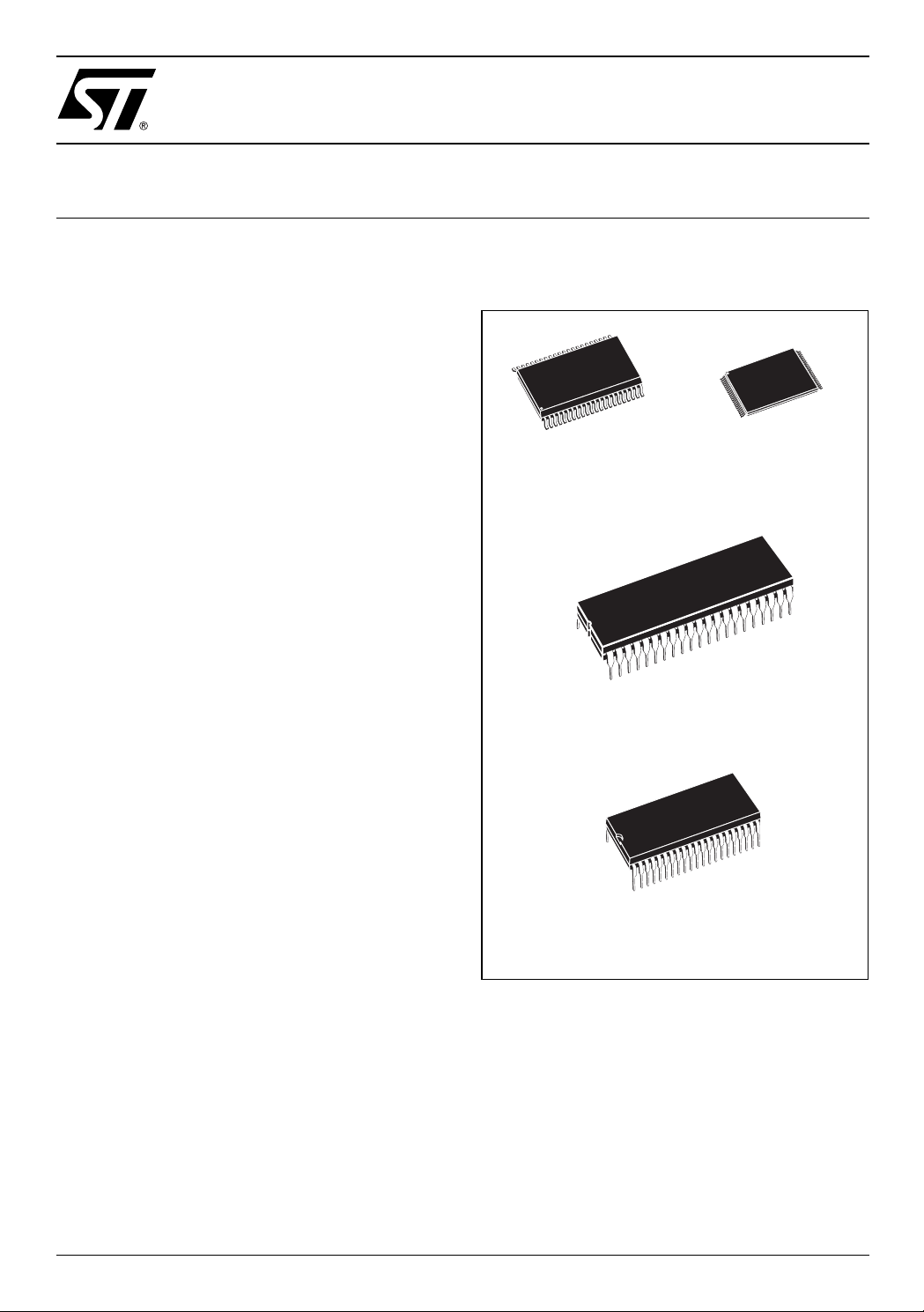
Figure 1. Packages
SO44 (M)
42
1
M27W016
TSOP48 (N)
12 x 20mm
PDIP42 (B)
42
1
SDIP42 (S)
1/26March 2003

M27W016
TABLE OF CONTENTS
FEATURES SUMMARY . . . . . . . . . . . . . . . . . . . . . . . . . . . . . . . . . . . . . . . . . . . . . . . . . . . . . . . . . . . . . 1
Figure 1. Packages . . . . . . . . . . . . . . . . . . . . . . . . . . . . . . . . . . . . . . . . . . . . . . . . . . . . . . . . . . . . . . 1
Figure 2. Logic Diagram . . . . . . . . . . . . . . . . . . . . . . . . . . . . . . . . . . . . . . . . . . . . . . . . . . . . . . . . . . 4
Table 1. Signal Names . . . . . . . . . . . . . . . . . . . . . . . . . . . . . . . . . . . . . . . . . . . . . . . . . . . . . . . . . . . 4
Figure 3. PDIP Connections . . . . . . . . . . . . . . . . . . . . . . . . . . . . . . . . . . . . . . . . . . . . . . . . . . . . . . . 5
Figure 4. SDIP Connections . . . . . . . . . . . . . . . . . . . . . . . . . . . . . . . . . . . . . . . . . . . . . . . . . . . . . . . 5
Figure 5. SO Connections. . . . . . . . . . . . . . . . . . . . . . . . . . . . . . . . . . . . . . . . . . . . . . . . . . . . . . . . . 6
Figure 6. TSOP Connections . . . . . . . . . . . . . . . . . . . . . . . . . . . . . . . . . . . . . . . . . . . . . . . . . . . . . . . 6
SIGNAL DESCRIPTIONS . . . . . . . . . . . . . . . . . . . . . . . . . . . . . . . . . . . . . . . . . . . . . . . . . . . . . . . . . . . . 7
Address Inputs (A0-A19). . . . . . . . . . . . . . . . . . . . . . . . . . . . . . . . . . . . . . . . . . . . . . . . . . . . . . . . . . 7
Data Inputs/Outputs (DQ0-DQ7). . . . . . . . . . . . . . . . . . . . . . . . . . . . . . . . . . . . . . . . . . . . . . . . . . . . 7
Data Inputs/Outputs (DQ8-DQ15 ). . . . . . . . . . . . . . . . . . . . . . . . . . . . . . . . . . . . . . . . . . . . . . . . . . . 7
Chip Enable (E). . . . . . . . . . . . . . . . . . . . . . . . . . . . . . . . . . . . . . . . . . . . . . . . . . . . . . . . . . . . . . . . . 7
Output Enable (G). . . . . . . . . . . . . . . . . . . . . . . . . . . . . . . . . . . . . . . . . . . . . . . . . . . . . . . . . . . . . . . 7
V
Supply Voltage. . . . . . . . . . . . . . . . . . . . . . . . . . . . . . . . . . . . . . . . . . . . . . . . . . . . . . . . . . . . . . 7
CC
Program Supply Voltage . . . . . . . . . . . . . . . . . . . . . . . . . . . . . . . . . . . . . . . . . . . . . . . . . . . . . . 7
V
PP
Vss Ground.. . . . . . . . . . . . . . . . . . . . . . . . . . . . . . . . . . . . . . . . . . . . . . . . . . . . . . . . . . . . . . . . . . . . 7
BUS OPERATIONS. . . . . . . . . . . . . . . . . . . . . . . . . . . . . . . . . . . . . . . . . . . . . . . . . . . . . . . . . . . . . . . . . 8
Bus Read. . . . . . . . . . . . . . . . . . . . . . . . . . . . . . . . . . . . . . . . . . . . . . . . . . . . . . . . . . . . . . . . . . . . . . 8
Bus Write. . . . . . . . . . . . . . . . . . . . . . . . . . . . . . . . . . . . . . . . . . . . . . . . . . . . . . . . . . . . . . . . . . . . . . 8
Output Disable. . . . . . . . . . . . . . . . . . . . . . . . . . . . . . . . . . . . . . . . . . . . . . . . . . . . . . . . . . . . . . . . . . 8
Standby. . . . . . . . . . . . . . . . . . . . . . . . . . . . . . . . . . . . . . . . . . . . . . . . . . . . . . . . . . . . . . . . . . . . . . . 8
Automatic Standby. . . . . . . . . . . . . . . . . . . . . . . . . . . . . . . . . . . . . . . . . . . . . . . . . . . . . . . . . . . . . . . 8
Electronic Signature. . . . . . . . . . . . . . . . . . . . . . . . . . . . . . . . . . . . . . . . . . . . . . . . . . . . . . . . . . . . . .8
Table 2. Bus Operations . . . . . . . . . . . . . . . . . . . . . . . . . . . . . . . . . . . . . . . . . . . . . . . . . . . . . . . . . . 8
COMMAND INTERFACE . . . . . . . . . . . . . . . . . . . . . . . . . . . . . . . . . . . . . . . . . . . . . . . . . . . . . . . . . . . . 9
Read/Reset Command.. . . . . . . . . . . . . . . . . . . . . . . . . . . . . . . . . . . . . . . . . . . . . . . . . . . . . . . . . . . 9
Auto Select Command. . . . . . . . . . . . . . . . . . . . . . . . . . . . . . . . . . . . . . . . . . . . . . . . . . . . . . . . . . . . 9
Word Program Command.. . . . . . . . . . . . . . . . . . . . . . . . . . . . . . . . . . . . . . . . . . . . . . . . . . . . . . . . . 9
Multiple Word Program Command . . . . . . . . . . . . . . . . . . . . . . . . . . . . . . . . . . . . . . . . . . . . . . . . . .9
Setup Phase.. . . . . . . . . . . . . . . . . . . . . . . . . . . . . . . . . . . . . . . . . . . . . . . . . . . . . . . . . . . . . . . . 9
Program Phase. . . . . . . . . . . . . . . . . . . . . . . . . . . . . . . . . . . . . . . . . . . . . . . . . . . . . . . . . . . . . . 9
Verify Phase. . . . . . . . . . . . . . . . . . . . . . . . . . . . . . . . . . . . . . . . . . . . . . . . . . . . . . . . . . . . . . . . 1 0
Exit Phase. . . . . . . . . . . . . . . . . . . . . . . . . . . . . . . . . . . . . . . . . . . . . . . . . . . . . . . . . . . . . . . . . 10
Table 3. Standard Commands . . . . . . . . . . . . . . . . . . . . . . . . . . . . . . . . . . . . . . . . . . . . . . . . . . . . . 1 1
Table 4. Multiple Word Program Command . . . . . . . . . . . . . . . . . . . . . . . . . . . . . . . . . . . . . . . . . . 11
Table 5. Program Times . . . . . . . . . . . . . . . . . . . . . . . . . . . . . . . . . . . . . . . . . . . . . . . . . . . . . . . . . 11
Figure 7. Multiple Word Program Flowchart . . . . . . . . . . . . . . . . . . . . . . . . . . . . . . . . . . . . . . . . . . 12
2/26

M27W016
STATUS REGISTER. . . . . . . . . . . . . . . . . . . . . . . . . . . . . . . . . . . . . . . . . . . . . . . . . . . . . . . . . . . . . . . 13
Data Polling Bit (DQ7). . . . . . . . . . . . . . . . . . . . . . . . . . . . . . . . . . . . . . . . . . . . . . . . . . . . . . . . . . . 13
Toggle Bit (DQ6).. . . . . . . . . . . . . . . . . . . . . . . . . . . . . . . . . . . . . . . . . . . . . . . . . . . . . . . . . . . . . . . 13
Error Bit (DQ5). . . . . . . . . . . . . . . . . . . . . . . . . . . . . . . . . . . . . . . . . . . . . . . . . . . . . . . . . . . . . . . . . 13
V
Status Bit (DQ4). . . . . . . . . . . . . . . . . . . . . . . . . . . . . . . . . . . . . . . . . . . . . . . . . . . . . . . . . . . . 13
PP
Multiple Word Program Bit (DQ0) . . . . . . . . . . . . . . . . . . . . . . . . . . . . . . . . . . . . . . . . . . . . . . . . . . 13
Multiple Word Program Bit (DQ0) . . . . . . . . . . . . . . . . . . . . . . . . . . . . . . . . . . . . . . . . . . . . . . . . . . 13
Table 6. Status Register Bits. . . . . . . . . . . . . . . . . . . . . . . . . . . . . . . . . . . . . . . . . . . . . . . . . . . . . . 14
Figure 8. Data Polling Flowchart . . . . . . . . . . . . . . . . . . . . . . . . . . . . . . . . . . . . . . . . . . . . . . . . . . . 1 4
Figure 9. Data Toggle Flowchart. . . . . . . . . . . . . . . . . . . . . . . . . . . . . . . . . . . . . . . . . . . . . . . . . . . 1 4
MAXIMUM RATING. . . . . . . . . . . . . . . . . . . . . . . . . . . . . . . . . . . . . . . . . . . . . . . . . . . . . . . . . . . . . . . . 15
Table 7. Absolute Maximum Ratings. . . . . . . . . . . . . . . . . . . . . . . . . . . . . . . . . . . . . . . . . . . . . . . .15
DC and AC PARAMETERS . . . . . . . . . . . . . . . . . . . . . . . . . . . . . . . . . . . . . . . . . . . . . . . . . . . . . . . . . 1 6
Table 8. Operating and AC Measurement Conditions. . . . . . . . . . . . . . . . . . . . . . . . . . . . . . . . . . . 16
Figure 10. AC Measurement I/O Waveform . . . . . . . . . . . . . . . . . . . . . . . . . . . . . . . . . . . . . . . . . . 16
Figure 11. AC Measurement Load Circuit. . . . . . . . . . . . . . . . . . . . . . . . . . . . . . . . . . . . . . . . . . . . 16
Table 9. Device Capacitance. . . . . . . . . . . . . . . . . . . . . . . . . . . . . . . . . . . . . . . . . . . . . . . . . . . . . . 16
Table 10. DC Characteristics. . . . . . . . . . . . . . . . . . . . . . . . . . . . . . . . . . . . . . . . . . . . . . . . . . . . . . 17
Figure 12. Read AC Waveforms . . . . . . . . . . . . . . . . . . . . . . . . . . . . . . . . . . . . . . . . . . . . . . . . . . . 18
Table 11. Read AC Characteristics . . . . . . . . . . . . . . . . . . . . . . . . . . . . . . . . . . . . . . . . . . . . . . . . . 18
Figure 13. Chip Enable Controlled, Write AC Waveforms. . . . . . . . . . . . . . . . . . . . . . . . . . . . . . . . 19
Table 12. Chip Enable Controlled, Write AC Characteristics . . . . . . . . . . . . . . . . . . . . . . . . . . . . . 19
PACKAGE MECHANICAL . . . . . . . . . . . . . . . . . . . . . . . . . . . . . . . . . . . . . . . . . . . . . . . . . . . . . . . . . . 20
SO44 - 44 lead Plastic Small Outline, 500 mils body width, Package Outline . . . . . . . . . . . . . . . . 20
SO44 - 44 lead Plastic Small Outline, 500 mils body width, Package Mechanical Data . . . . . . . . . 20
TSOP48 - 48 lead Plastic Thin Small Outline, 12 x 20mm, Package Outlin e . . . . . . . . . . . . . . . . . 21
TSOP48 - 48 lead Plastic Thin Small Outline, 12 x 20mm, Package Me chanical Data . . . . . . . . . 21
PDIP42 - 42 pin Plastic DIP, 600 mils width, Bottom View Package Outline . . . . . . . . . . . . . . . . . 22
PDIP42 - 42 pin Plastic DIP, 600 mils width, Package Mechanical Data . . . . . . . . . . . . . . . . . . . . 22
SDIP42 - 42 pin Shrink Plastic DIP, 600 mils width, Package Outline . . . . . . . . . . . . . . . . . . . . . . 23
SDIP42 - 42 pin Shrink Plastic DIP, 600 mils width, Package Mechanical Data. . . . . . . . . . . . . . .23
PART NUMBERING . . . . . . . . . . . . . . . . . . . . . . . . . . . . . . . . . . . . . . . . . . . . . . . . . . . . . . . . . . . . . . . 24
Table 17. Ordering Information Scheme. . . . . . . . . . . . . . . . . . . . . . . . . . . . . . . . . . . . . . . . . . . . .24
REVISION HISTORY . . . . . . . . . . . . . . . . . . . . . . . . . . . . . . . . . . . . . . . . . . . . . . . . . . . . . . . . . . . . . . . 25
Table 18. Document Revision History . . . . . . . . . . . . . . . . . . . . . . . . . . . . . . . . . . . . . . . . . . . . . . .25
3/26
M27W016
SUMMARY DESCRIPTION
The M27W016 is a 16 Mbit (2Mb x16) non-volatile,
One Time Programmable (OT P), FlexibleROM™
Memory. Read operations can be performed using
a single low voltage (2.7 to 3.6V) supply. Program
operations require an additional V
(11.4 to
PP
12.6V) power supply. On power-up the memory
defaults to Read mode where it can be read in the
same way as a ROM or EPROM.
Program commands are written to t he Command
Interface of the memory. An on-chip Program Controller (PC) simplifies the process of programming
the memory by taking care of all of the special operations that are required to update the memory
conte nts.
The M27W016 features an in novative command,
Multiple Word Program, used to program large
streams of data. It greatly reduces the total pro-
Figure 2. Logic Diagram Table 1. Signal Names
gramming time when a large number of Words are
written to the memory at any one time. Using this
command the entire memory can be program m ed
in 2s, compared to 9s using the standard Word
Progra m.
The end of a program operation can be de tected
and any error conditions identified. The command
set required to control the memory is consistent
with JEDEC standards.
Chip Enable and Output Enable signals control the
bus operation of the memory. They allo w simple
connection to most microprocessors, often without
additional logic.
The memory is offered in SO44, TSOP48 (12 x
20mm), PDIP42 and SDIP42 packages. The
memory is supplied with all the bits set to ’1’.
A0-A19 Address Inputs
V
V
20
A0-A19 DQ0-DQ15
E
G
M27W016
V
CC
SS
PP
16
AI05906
DQ0-DQ15 Data Inputs/Outputs
E
G
V
CC
V
PP
V
SS
NC Not Connected Internally
Chip Enable
Output Enable
Supply Voltage read
Supply Voltage program
Ground
4/26
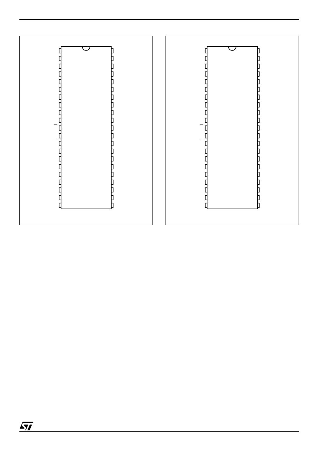
Figure 3. PDIP Connection s Figure 4. SDIP Connection s
M27W016
A18
A17
A7
A6
A5
A4
A3
A2
A1
A0
V
SS
DQ0
DQ8
DQ1
DQ9
DQ2
DQ10
DQ3
DQ11
1
2
3
4
5
6
7
8
9
10
M27W016
11
E
12
13
G
14
15
16
17
18
19
20
21
AI05907
42
41
40
39
38
37
36
35
34
33
32
31
30
29
28
27
26
25
24
23
22
A19
A8
A9
A10
A11
A12
A13
A14
A15
A16
V
PP
V
SS
DQ15
DQ7
DQ14
DQ6
DQ13
DQ5
DQ12
DQ4
V
CC
A18
A17
A7
A6
A5
A4
A3
A2
A1
A0
V
SS
DQ0
DQ8
DQ1
DQ9
DQ2
DQ10
DQ3
DQ11
1
2
3
4
5
6
7
8
9
10
M27W016
11
E
12
13
G
14
15
16
17
18
19
20
21
AI05907
42
41
40
39
38
37
36
35
34
33
32
31
30
29
28
27
26
25
24
23
22
A19
A8
A9
A10
A11
A12
A13
A14
A15
A16
V
PP
V
SS
DQ15
DQ7
DQ14
DQ6
DQ13
DQ5
DQ12
DQ4
V
CC
5/26
M27W016
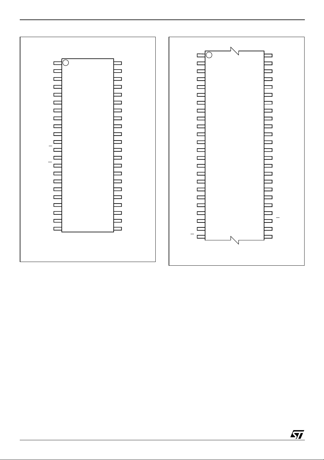
Figure 5. SO Connection s Figure 6. TSOP Connection s
NC
A18
A17 A8
A7
A6
A5
A4
A3
A2
A1
A0
V
SS
DQ0
DQ8
1
2
3
4
5
6
7
8
9
10
11
M27W016
12
E
13
14
G
15
16
17DQ1
DQ9
18
19
DQ10
DQ3
20
21
DQ11
44
43
42
41
40
39
38
37
36
35
34
33
32
31
30
29
28
27
26
25
24
2322
NC
A19
A9
A10
A11
A12
A13
A14
A15
A16
V
PP
V
SS
DQ15
DQ7
DQ14
DQ6
DQ13
DQ5DQ2
DQ12
DQ4
V
CC
AI05909
V
PP
A16
A15
A14
A13
A12
A11
A10
A9
A8
A19
V
SS
NC
A18
A17
A5
A0
A7
A6
A4
A3
A2
A1
1
12
M27W016
13
24 25
E
48
37
36
V
SS
V
SS
DQ15
DQ7
DQ14
DQ6
DQ13
DQ5
DQ12
DQ4
V
CC
V
CC
NC
DQ11
DQ3
DQ10
DQ2
DQ9
DQ1
DQ8
DQ0
G
V
SS
V
SS
AI05917
6/26

SIGNAL DESCRIPTIONS
See Figure 2, Logic Diagram, and Table 1, Sign al
Names, for a brief overview of the signals connected to this device.
Address Inputs (A0-A19). The Address Inputs select the cells i n the memory array to a ccess during Bus Read operations. During Bus Write operations they control the commands sent to the Command Interface of the Program Controller.
Data Inputs/Outputs (DQ0-DQ7). The Data Inputs/Outputs output the data stored at the selected address during a Bus Read operation. During Bus Write operations they represent the command sent to the Command Interface of the Program Controller. When reading the Status Register they report the status of the ongoing algorithm.
Data Inputs/Outputs (DQ8-DQ15). The Data Inputs/Outputs output the data stored at the selected address during a Bus Read operation. During Bus Write operations the Command Interface does not use these bits. When reading t he Status Register these bits should be ignored.
Chip Enable (E
). The Chip Enable, E, activates
the memory, allowing Bus Read operat ions to be
performed. It also controls the B us Write operations, when V
Output Enable (G
is in the VHH range.
PP
). The Ou tput Enable, G, con-
trols the Bus Read operations of the memory. It
M27W016
also allows Bus Write operations, when V
the V
V
range.
HH
Supply Voltage. The VCC Supply Voltage
CC
supplies the power for Read operations.
A 0.1µF ca pacitor should be connected between
the V
Supply Voltage pin and the VSS Ground
CC
pin to decouple the current surges from the power
supply. The PCB track widths must be sufficient to
carry the currents required during program operations, I
V
PP
.
CC3
Program Supply Voltage. VPP is both a
power supply and Write Protect pin. The two functions are selected by t he voltage range a pplie d to
the pin.
When the V
is in the VHH range (see Table 10,
PP
DC Characteristic, for the relevant values) the Program operation is enabled. During such operations the V
If the V
must be stable in the VHH range.
PP
is kept under the VHH range, particularly
PP
in the voltage range 0 to 3.6V, any Program operation is disabled or stopped.
Note that V
must not be left floating o r uncon-
PP
nected as the device may become unreliable. Vss Ground. The V
Ground is the reference
SS
for all voltage measurements.
PP
is in
7/26
M27W016
BUS OPERATIONS
There are six standard bus operations that control
the device. These are Bus Read, Bus Wri te, Output Disable, Standby, Automatic Standby and
Electronic Signature. See Tables 2, Bus Operations, for a summary. Typically glitches of less
than 5ns on Chip Enable or Write Enable are ignored by the memory and do not affect bus operations.
Bus Read. Bus Read operations read from the memory cells, or specific registers in the Command Interface. A valid Bus Read operation involves setting the desired address on the Address Inputs and applying a Low signal, V able and Output Enable. The Data Inputs/Outpu ts will output the value, see Figure 12, Read AC Waveforms, and Table 11, Read AC Ch aracteristics, for details of when the output becomes valid.
Bus Write. Bus Write operations write to the Command Interface. Bus Write is enabled only when V
is set to VHH. A valid Bus W rite opera-
PP
tion begins by setting the desired addres s on the
Address Inputs. The Address Inputs are latched by
the Command Interface on the falling edge of Chip
Enable. The Data I nputs/Outputs are latched by
the Command Interface on the rising edge of Chip
Enable. Output Enable must remain High, V
during the whole Bus W rite operat ion . See Fi gure
13, Write AC Waveforms, and Table 12, Write AC
Characteristics, for details of the timing requirements.
, to Chip En-
IL
IH
Output Disa bl e . The Data Inputs/Outputs are in the high impedance s tate when Output Enable is High, V
.
IH
Standby. When Chip Enable is High, V memory enters Standby mode and the Data Inputs/Outputs pins are placed in the high-impedance state. To reduce the S upply Current to the Standby Supply Current, I be held within V
± 0.2V. For the Standby current
CC
, Chip Enable should
CC2
level see Table 10, DC Characteristics.
During program operation the mem ory will cont in-
ue to use the Program Supply Current, I
Program operation until the operation completes.
Automatic Standby. If CMOS levels (V are used to drive the bus and the bus is inactive for 150ns or more the memory enters Automatic Standby where the internal Supply Current is reduced to the Standby Supply Current, I Data Inputs/Outputs will still output data if a Bus Read operation is in progress.
Electronic Signature. The memory has two codes, the manufacturer code and the device code, that can be read to identify the memory. These codes can be read by applying t he signals listed in Tables 2, Bus Operat ions, once the A uto
,
Select Command is executed. To exit Electronic
Signature mode, the Read/Reset c ommand must
be issued.
CC3
± 0.2V)
CC
CC2
, the
IH
. The
, for
Table 2. Bus Operations
Operation E G
HH
V
IL
V
IL
V
IH
V
IL
V
IL
Bus Read
Bus Write
Output Disable X
Standby
Read Manufacturer
Code
Read Device Code
Note: 1. X = VIL or VIH.
2. XX = V
3. When reading Statu s Register during Program algori thm execution VPP must be kept at VHH.
, V
or V
IL
IH
V
IL
V
IH
V
IH
X X X Hi-Z
V
IL
V
IL
V
PP
(3)
XX
V
HH
X X Hi-Z
V
HH
V
HH
Address Inputs
A0-A19
Cell Address Data Output
Command Address Data Input
A0 = VIL, A1 = VIL,
Others VIL or V
A0 = VIH, A1 = VIL,
Others VIL or V
IH
IH
Data Inputs/Outputs
DQ15-DQ0
0020h
888Dh
8/26

COMMAND INTERFACE
All Bus Write operations t o the me mory are in terpreted by the Command Interface. Commands
consist of one or more sequential Bus Write operations. Failure to observe a valid sequence of Bus
Write operations will result in the memory returning to Read mode. The long command sequences
are imposed to maximize data security.
Refer to Tables 3 and 4, for a summary of the commands.
Read/Reset Command.
The Read/Reset command returns the memory to
its Read mode where it behaves like a ROM or
EPROM, unless otherwise stated. It also resets
the errors in the Status Register. Either one or
three Bus Write operations can be u sed to issue
the Read/Reset command.
must be set to VHH during the Read/Reset
V
PP
command. If V
is set to either V
PP
IL
or V
the com-
IH
mand will be ignored. The command can be issued, between Bus Write cycles before the start of
a program operation, to return the device to read
mode. Once the program operation has started the
Read/Reset command is no longer accepted.
Auto Select Command.
The Auto Select command is used to read the
Manufacturer Code and the Device Code. V
PP
must be set to VHH during the Auto Select command. If V
is set to either V
PP
IL
or V
the com-
IH
mand will be ignored. Three consecutive Bus
Write operations are required to issue the Auto Select command. Once the Auto Select command is
issued the memory remai ns in Auto Select m ode
until a Read/Reset com mand is issued, all other
commands are ignored.
From the Auto Select mode the Manufacturer
Code can be read using a Bus Read operation
with A0 = VIL and A1 = VIL. The other address bits
may be set to either V
or VIH.
IL
The Device Code can be read using a B us Read
operation with A0 = V
address bits may be set to either V
and A1 = VIL. The other
IH
or VIH.
IL
Word Progr a m Com m a n d.
The Word Program command can be used to program a Word to the memory array. V
set to V
ther V
during Word Program. If VPP is set to ei-
HH
or VIH the command will be ignored, the
IL
must be
PP
data will remain unchanged and the device will revert to Read/Reset mode. The command requires
four Bus Write operations, the final write operation
latches the address and data in the internal state
machine and starts the PC.
During the program operat ion the memo ry will ignore all commands. I t is n ot poss ible t o iss ue any
command to abort or pause the operation. Typical
program times are given in Table 5. Bus Read op-
M27W016
erations during the program o peration will output
the Status Register on the Data Inputs/Outputs.
See the section on the S tatus Register for more
details.
After the program operation has completed the
memory will return to the Read mode, unle ss an
error has occurred. When an error occurs the
memory will continue to output the Status Register. A Read/Reset command must be issued to reset the error condition and return to Read mode.
Note that the Program command cannot change a
bit set at ’0’ back to ’1’.
Multiple Word Program Command
The Multiple Word Program command can be
used to program large streams of data. It greatly
reduces the total programming time when a l arge
number of Words are written in the memory at
once. V
Program. If V
mand will be ignored, the data will remain unchanged and the device will revert to Read mode.
It has four phases: the Setup P hase to initiate the
command, the Program Phase to program the
data to the memory, the Verify Phase to check that
the data has been correctly programmed and reprogram if necessary and the Exit Phase.
Setup Phase. The M ultiple Word Program command requires three Bus Write operations to initiate the command (refer to Table 4, Multiple Word Program Command and Figure 8, Multiple Word Program Flowchart).
The Status Register must be read in order to
check that the PC has started (see Table 6 and
Figure 8).
Program Phase. The Program Phase requires n+1 Bus Write operations, where n is the num ber of Words, to execute t he program mi ng p has e (refer to Table 4, Multiple Word Program and Figure 7, Multiple Word Program Flowchart).
Before any Bus Write operation of the Program
Phase, the Status Register m ust be read i n order
to check that the PC is ready to accept the operation (see Table 6 and Figure 8).
The Program Phase is executed in three different
sub-phases:
1. The first Bus Write operation of the Program
Phase (the 4th of the command) latches the
Start Address and the first Word to be
programmed.
2. Each subs equent Bus Write operation latches
the next Word to be programmed and
automatically increments the internal Address
Bus. It is not necessary to provide the address
of the location to be programmed but only a
Continue Address, CA (A17 to A19 equal to the
must be set to VHH during Multiple Word
PP
is set either VIL or VIH the com-
PP
9/26

M27W016
Start Address), that indicates to the PC that the
Program Phase has to continue. A0 to A16 are
‘don’t car e’.
3. Finally, after all Words have been programmed,
a Bus Write operation (the (n+1)
th
) with a Final
Address, FA (A17 or a higher address pin
different from the Start Address), ends the
Program Phase.
The memory is now set to enter the Verify Phase. Verify Phase. Th e Verify Phase is s imilar to the
Program Phase in that all Words must be resent to
the memory for them to be che cked against the
programmed data.
Before any Bus Write Operation of the Verify
Phase, the Status Register m ust be read i n order
to check that the PC is ready for the next operation
or if the reprogram of the location has failed (see
Table 6 and Figure 8).
Three successive steps are required to execute
the Verify Phase of the command:
1. The first Bus Write operation of the Verify Phase
latches the Start A ddress and the Word t o be
verified.
2. Each subs equent Bus Write operation latches
the next Word to be verified and automatically
increments the internal Address Bus. As in the
Program Phase, it is not necessary to provide
the address of the location to be program med
but only a Continue Address, CA (A17 to A 19
equal to the Start Address).
3. Finally, after all Words have been verified, a Bus
Write cycle with a Final Address, FA (A17 or a
higher address pin different from the Start
Address) ends the Verify Phase.
Exit Phase. After the Verify Phase ends, the Status Register must be read to check if the command has successfully completed or not (see Table 6 and Figure 8).
If the Verify Phase is suc cessful, the memory returns to Read mode and DQ6 stops toggling.
If the PC fails to reprogram a given location, the
Verify Phase terminates, DQ6 continues toggl ing
and error bit DQ5 is set in the Statu s Register. If
the error is due to a V
failure DQ4 is also set.
PP
When the operation fails a Read/Reset command
must be issued to return the device to Read mode.
During the Multiple Word Program operation the
memory will ignore all commands. It is not possible
to issue any command to abort or pause the operation. Typical program times are give n in T able 5.
Bus Read operations during the program operati on will output the Status Register on the Data Inputs/Outputs. See the section on the Status
Register for more details.
Note that the Multiple Word Program command
cannot change a bit set to ’0’ back to ’1’.
10/26

Table 3. Standard Commands
M27W016
Bus Write Operations
Command
Length
1st 2nd 3rd 4th
Add Data Add Data Add Data Add Data
1X F0
Read/Reset
3 555 AA 2AA 55 X F0
Auto Select 3 555 AA 2AA 55 555 90
Word Program 4 555 AA 2AA 55 555 A0 PA PD
Note: X Don’t Care, PA Program Address, PD Program Data. All values in the table are in hexadecimal. The Command Interface only uses
A0-A10 and DQ0-DQ7 to verify the commands; A11-A19, DQ8-D Q 15 are Don’t Care.
Table 4. Multiple Word Program Command
Bus Write Operations
Phase
Length
1st 2nd 3rd 4th 5th nth Final
Add Data Add Data Add Data Add Data Add Data Add Data Add Data
Set-Up 3 555 AA 2AA 55 555 20
Program n+1 SA PD1 CA PD2 CA PD3 CA PD4 CA PD5 CA PAn FA X
Verify n+1 SA PD1 CA PD2 CA PD3 CA PD4 CA PD5 CA PAn FA X
Note: A Bus Read must be done between each Write cycle where the data is programmed or verified, to Read the Status Register and check
that the memory is ready to accept the next data. SA is the Start Address. CA is the Continue Address. FA is the Final Address. X Don’t
Care, n = number of Words to be programmed.
Tabl e 5. Program Time s
Parameter
Typ
(1)
Max U nit
Program (Word) 9 200 µs
Chip Program (Multiple Word) 2 35 s
Chip Program (Word by Word) 9 35 s
Note: 1. TA = 25°C, VPP = 12V.
11/26

M27W016
Figure 7. Mul ti pl e W or d Program Fl owchart
Setup
Phase
NO
Setup time
exceeded?
EXIT (
Program
Phase
YES
setup failed)
Start
Write AAh
Address 555h
Write 55h
Address 2AAh
Write 20h
Address 555h
Read Status
Register
NO
DQ6
toggling?
YES
NO
DQ0 = 0?
YES
Write Data1
Start Address
Read Status
Register
DQ0 = 0?
YES
Write Data 2
Continue Address
Read Status
Register
DQ0 = 0?
Write Data n
Continue Address
Read Status
Register
DQ0 = 0?
YES
Write XX
Final Address
YES
NO
NO
NO
Read Status
Register
DQ0 = 0?
Write Data1
Start Address
Read Status
Register
DQ0 = 0?
YES
Write Data 2
Continue Address
Read Status
Register
DQ0 = 0?
YES
Write Data n
Continue Address
Read Status
Register
DQ0 = 0?
YES
Write XX
Final Address
Read Status
Register
DQ6
toggling?
NO
NO
NO
DQ5 = 1 ?
NO
DQ5 = 1?
NO
YES
DQ5 = 1?
Fail error
Exit (read mode)
Verify
Phase
NO
NO
NO
YES
YES
YES
YES
Read Status
Register
DQ4 = 0?
Write F0h
Address XX
Exit
Phase
NO
Fail, VPP error
12/26
AI05954b

STATUS REGISTER
Bus Read operations from any address always
read the Status Register during Program operations. The bits in the Status Regi ster are summ arized in Table 6, Status Register Bits.
Data Polling Bit (DQ7). The Data Polling Bit can be used to identify whether the Program Controller has successfully completed its operation. The Data Polling Bit is output on DQ7 when the Status Register is read.
During a Word Program operation the Data Polling
Bit outputs the complement of the bit being programmed to DQ7. After successful completion of
the Word Program ope ration the memory ret urns
to Read mode and Bus Read operations from the
address just programmed output DQ7, not its complement.
Figure 8, Data Polling Flowchart, gives an example of how to use the Data Polling Bit. A Valid Address is the address being programmed.
Toggle Bit (DQ6). The Toggle Bit can be used to identify whether the Program Con troller has successfully completed its operation. The Toggle Bit is output on DQ6 when the Status Register is read.
During Program operations the Toggle Bit changes from ’0’ to ’1’ to ’0’, etc., with successive Bus
Read operations at any address. After successful
completion of the operation the memory returns to
Read mode.
M27W016
Figure 9, Data Toggle Flowchart, g ives an example of how to use the Data Toggle Bit.
Error Bit (DQ5). The Error Bit can be used to identify errors detected by the Program Controller. The Error Bit is set to ’1’ when a Program operation fails to write the correct data to the memory. If the Error Bit is set a Re ad/Reset command m ust be issued before other commands are issued. The Error bit is output on DQ5 when the Status Register is read.
Note that the Program command cannot change a
bit set to ’0’ back to ’1’ and attempting to do so will
set DQ5 to ‘1’. A Bus Read operation to that address will show the bit is still ‘0’.
Status Bit (DQ4). The VPP Status Bit can be
V
PP
used to identify if any Program operation has failed
due to a V
any Program operation, the operation a borts and
DQ4 is set to ‘1’. If V
the Program operation, the operation completes
and DQ4 is set to ‘0’.
Multiple Word Program Bit (DQ0). The Multiple
Word Program Bit can be used to indicate whether
the Program Controller is active or inactive during
Multiple Word Program. When the P rogram Controller has written one Word and is ready to accept
the next Word, the bit is set to ‘0’.
Status Register Bit DQ1 is reserved.
error. If V
PP
falls below VHH during
PP
remains at V
PP
throughout
HH
13/26

M27W016
Table 6. Status Register Bits
Command
(1)
P.C. Status DQ7 DQ6 DQ5 DQ4 DQ3 DQ0
Programming – Toggle 0 – 0 1
Multiple Word Program
Word Program
Note: 1. Unspecified data bits shou l d be ignored.
2. DQ4 = 0 if V
≥ VHH during Pr ogram algori t hm executi on; DQ4 = 1 if VPP < VHH during Progr am al gorithm execution.
PP
Waiting for data – Toggle 0 – 0 0
Program fail – Toggle 1
Programming DQ7
Program error DQ7
Toggle 0 – 0 –
Toggle 1
(2)
(2)
Figure 8. Dat a Po ll i ng Fl o wc h a rt Figure 9. Dat a Toggle Flow c hart
DQ5 & DQ6
READ DQ6
TOGGLE
NO
READ DQ6
TOGGLE
START
READ
DQ6
=
DQ5
= 1
TWICE
DQ6
=
NO
YES
YES
NO
YES
START
READ DQ5 & DQ7
at VALID ADDRESS
DQ7
YES
=
DATA
NO
NO
DQ5
= 1
YES
READ DQ7
at VALID ADDRESS
DQ7
YES
=
DATA
NO
FAIL PASS
01
0–
14/26
AI03598
FAIL PASS
AI01370B

MAXIMUM RATI N G
Stressing the device ab ove the rating listed in t he
Absolute Maximum Ratings" table may cause permanent damage to the device. Exposure to Absolute Maximum Rating conditions for extended
periods may affect device reliability. These are
these or any other conditions above those indicated in the Operating sections of this specification is
not implied. Refer also to the STMicroelectronics
SURE Program and ot her relevant quality documents.
stress ratings only and operation of the dev ice at
Table 7. Absolute Maximum Ratings
Symbol Parameter Min Max Unit
T
BIAS
T
STG
V
IO
V
CC
V
PP
Note: 1. Minimum vol tage may un dershoot t o –2V for less than 20ns duri ng transitions.
2. Maximum voltage may overshoot to V
3. Maximum voltage m ay oversh oot to 14.0V for less t han 20ns during transitions. V
of 80hrs.
Temperature Under Bias –50 125 °C
Storage Temperature –65 150 °C
Input or Output Voltage
(1,2)
–0.6
V
+0.6
CC
Read Supply Voltage –0.6 4 V
Program Supply Voltage
CC
(3)
+2V for less than 20ns during transitions.
–0.6 13.5 V
must not remain at VHH for more than a total
PP
M27W016
V
15/26
M27W016
DC AND AC PARAMETERS
This section summarizes t he operating m easurement conditions, and the DC and AC characteristics of the device. The parameters in the DC and
AC characteristics Tables that follow, are derived
from tests performed under the Measurement
Table 8. Operating and AC Measurement Conditions
Conditions summarized in Table 8, Operating and
AC Measurement Conditions. Designers should
check that the operating cond itions in their circuit
match the operating conditions when relying on
the quoted parameters.
M27W016 Unit
Parameter
100, 110
Min Max
V
Read Supply Voltage
CC
Program Supply Voltage
V
PP
2.7 3.6 V
11.4 12.6 V
Ambient Operating Temperature 0 70 °C
Load Capacitance (C
)
L
30 pF
Input Rise and Fall Times 10 ns
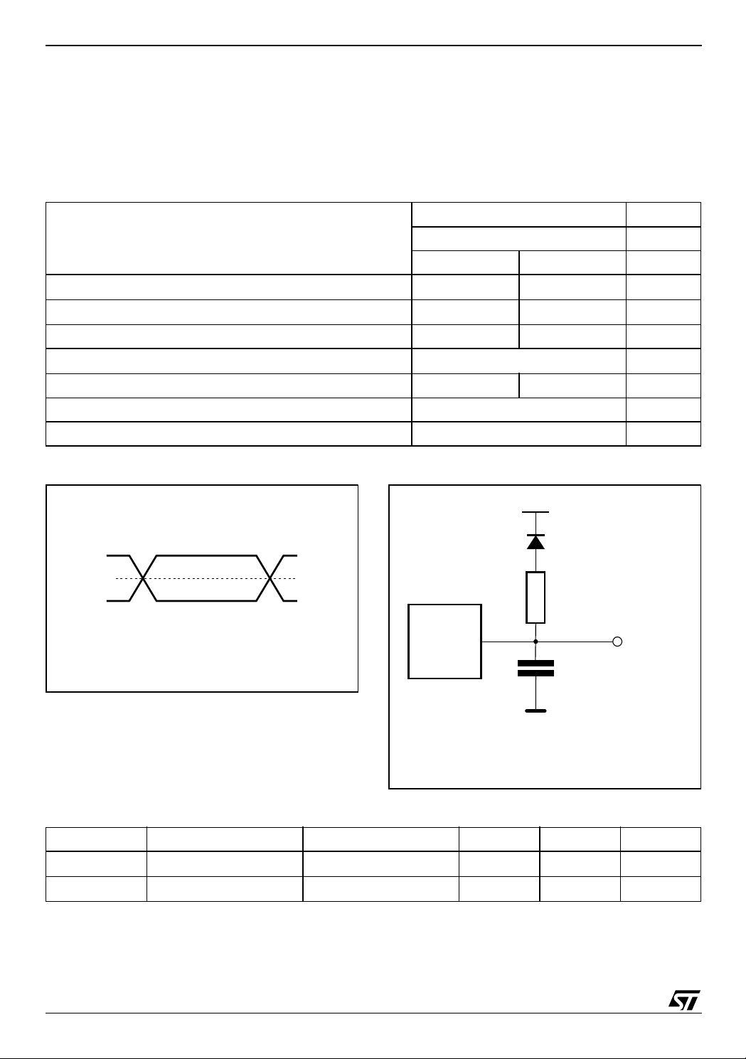
Input Pulse Voltages 0 to 3 V
Input and Output Timing Ref. Voltages 1.5 V
Figure 10. AC Measurem ent I/O W av eform Figure 11. AC Me a surement Lo a d Circuit
1.3V
3V
0V
1.5V
AI05546
DEVICE
UNDER
TEST
1N914
3.3kΩ
OUT
CL
CL = 30pF
CL includes JIG capacitance
Table 9. Device Capacitance
Symbol Parameter Test Condition Min Max Unit
C
IN
C
OUT
Note: Sampled only, not 100% tested.
Input Capacitance
Output Capacitance
16/26
V
V
OUT
IN
= 0V
= 0V
6pF
12 pF
AI05447

Table 10. DC Characteristics
Symbol
Parameter
(1)
M27W016
Test Condition Min Max Unit
0V ≤ V
I
OUT
0V ≤ V
E
E
I
I
LI
I
LO
I
CC1
I
CC2
I
CC3
V
IL
V
IH
V
OL
V
OH
V
HH
I
HH
Note: 1. VCC must be ap pl i ed simultaneously or before VPP and removed simult aneously or after VPP.
2. Average Va l ue.
Input Leakage Current
Output Leakage Current
Supply Current (Read)
(2)
Supply Current (Standby)
Supply Current (Program) PC active 20 mA
Input Low Voltage –0.5 0.8 V
Input High Voltage
Output Low Voltage
Output High Voltage
V
Program Voltage
PP
VPP Current (Program)
≤ V
IN
CC
≤ V
OUT
CC
= VIL, G = VIH,
= 0mA, f = 6MHz
= VCC ±0.2V
0.7V
I
= 1.8mA
OL
= –100µA
OH
V
CC
PC Active 10 mA
±1
µA
±1 µA
10 mA
CC
100
VCC +0.3
µA
0.45 V
–0.4
11.4 12.6 V
V
V
17/26

M27W016
Figure 12. Read AC Waveforms
A0-A19
tAVQV tAXQX
E
tELQV
G
DQ0-DQ15
VALID
tGLQV
Table 11. Read AC Characteristics
Symbol Alt
t
AVQVtACC
t
ELQVtCE
t
GLQVtOE
(2)
t
EHQZ
t
GHQZ
t
AXQXtOH
Note: 1. VPP must be applied after VCC and with the Chip Enable (E) at VIH.
t
HZ
(2)
t
DF
2. Sampled only, not 100% tested.
Parameter
Address Valid to
Output Valid
Chip Enable Low to
Output Valid
Output Enable Low to
Output Valid
Chip Enable High to
Output Hi-Z
Output Enable High to
Output Hi-Z
Address Transition to
Output Transition
(1)
T est Condition
= VIL,
E
G = V
= V
G
= V
E
= V
G
= V
E
Max 90 100 110 ns
IL
Max 90 100 110 ns
IL
Max353535ns
IL
Max303030ns
IL
Max303030ns
IL
Min 0 0 0 ns
VCC= 3.0 to 3.6V VCC = 2.7 to 3.6V VCC = 2.7 to 3.6V
tEHQZ
tGHQZ
VALID
AI05812
M27W016
Unit100 110
18/26

Figure 13. Chip Enable Controlled, Write AC Waveforms
M27W016
A0-A19
G
E
DQ0-DQ15
V
CC
V
PP
tAVEL
tVCHEL
tVPHEL
VALID
tELEHtGHEL
VALID
Table 12. Chip Enable Controlled, Write AC Characteristics
Symbol Alt
t
ELEH
t
DVEH
t
EHDX
t
EHEL
t
AVEL
t
ELAX
t
GHEL
t
EHGL
t
VCHEL
(2)
t
VPHEL
Note: 1. TA = 25°C; VPP = 11.4 to 12.6V. VCC = 2.7 to 3. 6V.
V
PP
Sampled only, not 100% tested.
2. Not requir ed i n Auto Selec t or Read/R eset comm and sequen ces.
t
t
t
t
CPH
t
t
Chip Enable Low to Chip Enable High Min 50 ns
CP
Input Valid to Chip Enable High Min 50 ns
DS
Chip Enable High to Input Transition Min 0 ns
DH
Chip Enable High to Chip Enable Low Min 50 ns
Address Valid to Chip Enable Low Min 0 ns
AS
Chip Enable Low to Address Transition Min 100 ns
AH
Output Enable High Chip Enable Low Min 10 ns
t
OEH
t
VCS
t
VCS
must be applied after VCC and with the Chip Enable (E) at VIH.
Chip Enable High to Output Enable Low Min 10 ns
VCC High to Chip Enable Low
VPP High to Chip Enable Low
Parameter
(1)
tELAX
tEHGL
tEHEL
tEHDXtDVEH
AI05583
M27W016 Unit
Min 50 µs
Min 500 ns
19/26

M27W016
PACKAGE MECHANICAL
Figure 14. SO44 - 44 lead Plastic Small Outline, 500 mils body width, Package Outline
D
44
23
c
E1
E
θ
1 22
LA1
A2
A
L1
ddd
b
e
SO-F
Note: Drawing is not to scale.
Table 13. SO44 - 44 lead Plastic Small Outline, 500 mils body width, Package Mechan ical Data
Symbol
Typ Min Max Typ Min Max
A 3.00 0.118
A1 0.10 0.004
millimeters inches
A2 2.69 2.56 2.79 0.1 06 0.101 0.110
b 0.35 0.50 0.014 0.020
c 0.18 0.28 0.007 0.011
D 28.50 28.37 28.63 1.122 1.117 1.127
ddd 0.10 0 .004
E 16.03 15.77 16.28 0.631 0.621 0.641
E1 12.60 12.47 12.73 0.4 96 0.491 0.501
e 1.27 – – 0.050 – –
L 0.79 0.031
L1 1.73 0.0 68
θ 8° 8°
N44 44
20/26

Figure 15. TSOP48 - 48 lead Plastic Thin Small Outline, 12 x 20mm, Package Outline
A2
1 N
e
E
B
N/2
M27W016
D1
D
DIE
A
CP
C
TSOP-a
Note: Drawing is not to scale.
LA1 α
Table 14. TSOP48 - 48 lead Plastic Thin Small Outline, 12 x 20mm, Package Mechanical Data
Symbol
Typ Min Max Typ Min Max
A 1.20 0.0472
A1 0.05 0.15 0.0020 0.0059
A2 0.95 1.05 0.0374 0.0413
B 0.17 0.27 0.0067 0.0106
C 0.10 0.21 0.0039 0 .0083
CP 0.10 0.0039
millimeters inches
D 19.80 20.20 0.7795 0 .7953
D1 18.30 18.50 0.7205 0.7283
E 11.90 12.10 0.4685 0.4764
e 0.50 – – 0.0197 – –
L 0.50 0.70 0.0197 0.0276
α 0° 5° 0° 5°
N48 48
21/26

M27W016
Figure 16. PDIP42 - 42 pin Plastic DIP, 600 mils width, Bottom View Package Outline
A2
A1AL
B1 B e1
D2
α
C
eA
eB
D
S
N
E1 E
1
Note: Drawing is not to scale.
PDIP
Table 15. PDIP42 - 42 pin Plastic DIP, 600 mils width, Package Mechanical Data
Symbol
Typ Min Max Typ Min Max
A – 5.08 – 0.200
A1 0.25 – 0. 010 –
A2 3.56 4.06 0.140 0.160
B 0.38 0.53 0. 015 0.021
B1 1.27 1.65 0.050 0.065
C 0.20 0.36 0.008 0.014
D 52.20 52.71 2.055 2.075
D2 50.80 – – 2.000 – –
E 15.24 – – 0.600 – –
E1 13.59 13.84 0.535 0.545
e1 2.54 – – 0.100 – –
eA 14.99 – – 0.590 – –
eB 15.24 17.78 0.600 0.700
L 3.18 3.43 0.125 0 .135
S 0.86 1.37 0. 034 0.054
α 0° 10° 0° 10°
N42 42
millimeters inches
22/26

Figure 17. SDIP42 - 42 pin Shrink Plastic DIP, 600 mils width, Package Outline
A2
A1AL
M27W016
b2 b e
D2
c
eA
eB
D
S
N
E1 E
1
Note: Drawing is not to scale.
SDIP
Table 16. SDIP42 - 42 pin Shrink Plastic DIP, 600 mils width, Package M echa nical Data
Symbol
Typ Min Max Typ Min Max
A 5.08 0 .200
A1 0.51 0.020
A2 3.81 3.05 4.57 0.1 50 0.120 0.180
millimeters inches
b 0.46 0.38 0.56 0.018 0.015 0.022
b2 1.02 0.89 1.14 0.0 40 0.035 0.045
c 0.25 0.23 0.38 0.010 0.009 0.015
D 36.83 36.58 37.08 1.450 1.440 1.460
e 1.78 – – 0.070 – –
E 15.24 16.00 0.600 0.630
E1 13.72 12.70 14.48 0.5 40 0.500 0.570
eA 15.24 – – 0.600 – –
eB 18.54 0.730
L 3.30 2.54 3.56 0.130 0.100 0.140
S 0.64 0.025
N42 42
23/26

M27W016
PART NUMBERING
Table 17. Ordering Information Scheme
Example: M27W016 100 N 1 T
Device Type
M27 = FlexibleROM™ Memory
Operating Voltage
W = V
Device Function
016 = 16 Mbit (x16)
Speed
100 = 100 ns
110 = 110 ns
Package
M = SO44, 500mils body width
N = TSOP48: 12 x 20 mm
B = PDIP42
S = SDIP42
= 2.7 to 3.6V
CC
(1)
Temperature Rang e
1 = 0 to 70 °C
Option
T = Tape & Reel Packing
Note: 1. This speed als o guarantees 90ns acc ess time at VCC = 3.0 to 3.6V.
Devices are shipped from the factory with all the bits set to ’1’.
For a list of available options (Speed, Pac kage, etc...) or for furthe r information on any aspect of this de-
vice, please contact the ST Sales Office nearest to you.
24/26

REVISION HIST ORY
Table 18. Document Revision History
Date Version Revision Details
28-Jan-2002 1.0 First Issue
Output Enable paragraph clarified
Electronic Signature paragraph clarified
Multiple Word Command paragraph clarified (Paragraph rewritten, Table 4, Figure 7)
15-May-2002 2.0
17-Jun-2002 3.0
Status Register Bits table clarified (Table 6)
SO44 package mechanical data and drawing clarified (Figure 14, Table 13)
PLCC44 package removed
Document status changed to Product Preview
Device classification changed to Fast OTP
Program Phase and Verify Phase paragraphs clarified
Standard Commands table clarified (Table 3)
Multiple Word Program Command table and Flowchart clarified (Table 4, Figure 7)
AC Measurement Load Circuit clarified (Figure 11)
Read AC parameters clarified (Figure 12, Table 11)
Chip Enable Controlled, Write AC parameters clarified (Figure 13, Table 12)
M27W016
28-Jun-2002 4.0
09-Jul-2002 5.0
31-Jul-2002 5.1
Document status changed to Preliminary Data
Document title clarified
100ns speed class added (90ns at V
= 3.0 to 3.6V)
CC
Product Name changed
Multiple Word Program Command Table clarified (Table 4)
I
, I
CC1
clarified (Table 10)
CC2
27-Sep-2002 5.2 Product Naming revised
Document status changed to Datasheet
OTP specification added
14-Nov-2002 5.3
SO44 package changed to 500mils body width
Bus Operation table clarified (Table 2)
Read/Reset , Auto Select and Multiple Word Program commands clarified
29-Nov-2002 5.4
90ns speed class obtained from the 100ns at V
and 12)
20-Feb-2003 5.5 T SOP Conn ection s diagram updat ed (Figure 6)
05-Mar-2003 5.6 Typing error on page 1 corrected
= 3.0 to 3.6V - clarifiication (T able 11
CC
25/26

M27W016
Information furnished is believed to be accurate and reliable. However, STMicroelectronics assumes no responsibility for the cons equences
of use of such information nor for any infringement of patents or other rights of third parties which may result from its use. No license is granted
by implic ation or o therwise under any patent or patent rights of STMicroelectron i cs. Speci fications mentioned i n this publication are subject
to change without notice. This publication supersedes and replaces all information previously supplied. STMicroelectronics products are not
authorized for use as c ri t i cal components in life support dev i ces or systems wi thout exp ress written approval of STMicroel ectronics.
The ST log o i s a registered tradema rk of STMicroelectronics
FlexibleR O M i s a pending trademark of S T M i croelectronics
All other nam es are the property of th ei r respect ive owners
© 2003 STMicroelectronics - All Rights Reserved
Australi a - Brazil - Canada - China - Finland - F rance - Germany - Hong Kong - India - Is rael - Italy - Japan - Malaysia - Malta -
Morocc o - Singapor e - Spain - Sweden - Switz erl and - Unit ed Kingdom - United States
STMicroelectron ics GROUP OF COMPANIES
www.st.com
26/26
 Loading...