

SGS Thomson Microelectronics M27V102 Datasheet
M27V102
1 Mbit (64Kbx 16) Low Voltage UV EPROM and OTP EPROM
LOW VOLTAGEREAD OPERATION:
3V to 3.6V
FASTACCESSTIME: 90ns
LOW POWERCONSUMPTION:
– Active Current 15mAat 5MHz
– StandbyCurrent 20µA
PROGRAMMING VOLTAGE:12.75V ± 0.25V
PROGRAMMINGTIME:100µs/byte (typical)
ELECTRONICSIGNATURE
– ManufacturerCode: 0020h
– Device Code: 008Ch
DESCRIPTION
The M27W102 is a low voltage 1 Mbit EPROM
offeredinthetworangesUV(ultravioleterase)and
OTP (one time programmable).It is ideallysuited
formicroprocessorsystemsrequiring large data or
programstorageandisorganizedas 65,536words
by 16 bits.
The M27V102 operates in the read mode with a
supply voltage as low as 3V. The decrease in
operating power allows either a reduction of the
size of the battery or an increase in the time between batteryrecharges.
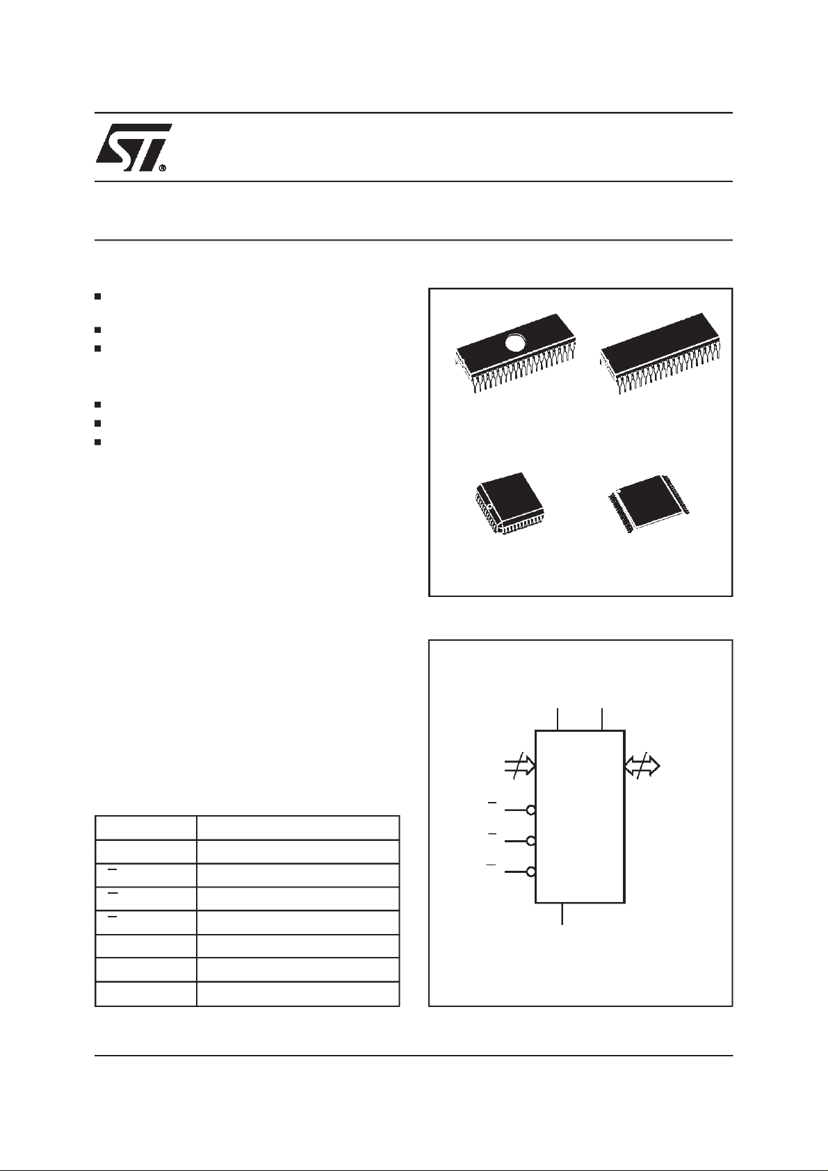
The FDIP40W(window ceramic frit-seal package)
has a transparent lid which allows the user to
expose the chip to ultraviolet light to erase the bit
pattern. A new pattern can then be written to the
deviceby following theprogramming procedure.
40
1
FDIP40W (F)
PLCC44 (K)
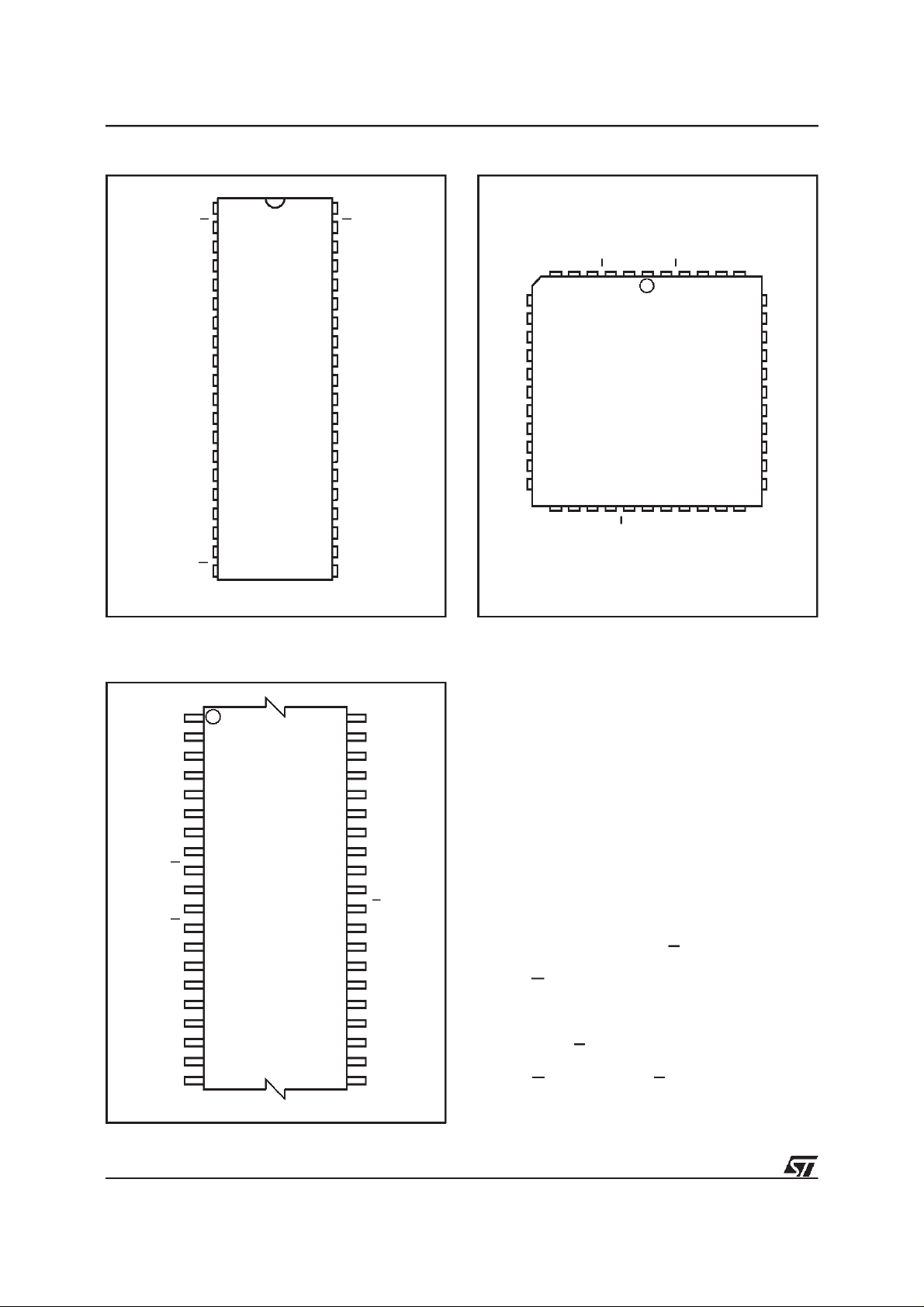
Figure1. Logic Diagram
V
16
A0-A15
CC
40
1
PDIP40 (B)
TSOP40 (N)
10 x 14mm
V
PP
16
Q0-Q15
Table 1. Signal Names
A0 - A15 Address Inputs
Q0 - Q15 Data Outputs
E Chip Enable
G Output Enable
P Program
V
PP
V
CC
V
SS
May 1998 1/15
Program Supply
Supply Voltage
Ground
P
E
G
M27V102
V
SS
AI01912
M27V102
Figure2A. DIPPin Connections
V
PP
Q15
Q14
Q13
Q12
Q11
Q10
Q9
Q8
V
SS
Q7
Q6
Q5
Q4
Q3
Q2
Q0
1
2
3
4
5
6
7
8
9
10
11
12
13
14
15
16
17
18
19
M27V102
40
39
38
37
36
35
34
33
32
31
30
29
28
27
26
25
24
23
22
2120
AI01913
V
CC
PE
NC
A15
A14
A13
A12
A11
A10
A9
V
SS
A8
A7
A6
A5
A4
A3
A2Q1
A1
A0G
Figure2B. LCC Pin Connections
Q15
Q13
Q14
Q12
Q11
Q10
Q9 A10
Q8
V
SS
NC
Q6
Q5
Q4
12
Q3
Q2
Q1
Q0
M27V102
CC
NC
VPPE
V
44
1
23
G
A0
NC
P
A1
NC
A2
A15
A3
A14
34
A4
A13
A12
A11
A9
V
SS
NC
A8Q7
A7
A6
A5
AI01914
Warning: NC = Not Connected.
Figure2C. TSOPPin Connections
A9
1
A10
A11
A12 A6
A13 A5
A14
A15
NC
P
V
CC
V
DQ15
DQ14
DQ13
DQ12 DQ4
DQ11 DQ5
DQ10
DQ9
DQ8
Warning: NC = Not Connected.
10
11
PP
E
20 21
M27V102
(Normal)
40
31
30
AI01915
V
SS
A8
A7
A4
A3
A2
A1
A0
G
DQ0
DQ1
DQ2
DQ3
DQ6
DQ7
V
SS
Warning: NC = Not Connected.
DESCRIPTION
(cont’d)
For application where the content is programmed
only one time and erasure is not required, the
M27V102 is offered in PDIP40, PLCC32 and
TSOP40(10 x 14 mm) packages.
DEVICEOPERATION
Theoperating modes of the M27V102are listedin
theOperating Modestable. Asingle powersupply
is required in the read mode. All inputs are TTL
levelsexcept for Vpp and 12V onA9 for Electronic
Signature.
ReadMode
The M27V102 has two control functions, both of
whichmustbelogicallyactiveinordertoobtaindata
attheoutputs. ChipEnable(E) isthepowercontrol
and should be used for device selection. Output
Enable(G)isthe outputcontrolandshouldbe used
to gate data to the output pins, independent of
deviceselection. Assumingthatthe addressesare
stable,the addressaccesstime(t
thedelayfrom Etooutput(t
at the output after a delay of t
). Datais available
ELQV
OE
) is equal to
AVQV
from the falling
edge of G, assuming that E has been low and the
addresses have been stable for at least t
.
t
GLQV
AVQV
-
2/15
M27V102
Table 2. Absolute MaximumRatings
(1)
Symbol Parameter Value Unit
T
A
T
BIAS
T
STG
V
IO
V
CC
V
A9
V
PP
Notes: 1. Except for therating ”Operating Temperature Range”, stresses above those listed in theTable ”AbsoluteMaximum Ratings”
2. Minimum DC voltage on Input or Output is –0.5V withpossible undershootto –2.0Vfor a periodless than 20ns. Maximum DC
3. Depends on range.
Ambient Operating Temperature
Temperature Under Bias –50 to 125
Storage Temperature –65 to 150 °C
(2)
Input or Output Voltages (except A9) –2 to 7 V
Supply Voltage –2 to 7 V
(2)
A9 Voltage –2 to 13.5 V
Program Supply Voltage –2 to 14 V
may cause permanent damage to thedevice. These are stress ratings only and operation of the device at these or any other
conditions above those indicatedin the Operating sections of this specification is not implied. Exposure to Absolute Maximum
Rating conditions for extendedperiods may affectdevice reliability.Refer also to the STMicroelectronics SURE Programand other
relevant qualitydocuments.
voltage on Output is V
+0.5Vwith possible overshoot to VCC+2V for a periodless than 20ns.
CC
(3)
–40 to 125 °C
°
C
Table 3. OperatingModes
Mode E G P A9 V
Read V
Output Disable V
Program V
Verify V
Program Inhibit V
Standby V
Electronic Signature V
Note: X=VIHor VIL,VID= 12V±0.5V
PP
IL
IL
IL
IL
IH
IH
IL
V
IL
V
IH
XV
V
IL
XXXVPPHi-Z
XXXV
V
IL
V
IH
XXV
Pulse X V
IL
V
IH
V
IH
XV
CC
CC
or V
or V
PP
SS
SS
XVPPData Output
or V
CC
SS
V
ID
V
CC
Q0 - Q15
Data Output
Hi-Z
Data Input
Hi-Z
Codes
Table 4. ElectronicSignature
Identifier A0 Q7 Q6 Q5 Q4 Q3 Q2 Q1 Q0 Hex Data
Manufacturer’s Code V
Device Code V
IL
IH
00100000 20h
10001100 8Ch
StandbyMode
TheM27V102hasastandbymode whichreduces
the active current from 15mA to 20µA with low
voltageoperationV
≤ 3.6V,see Read Mode DC
CC
Characteristics table for details. The M27V102 is
placedin thestandbymodeby applyinga TTLhigh
signal to the E input. When in the standby mode,
the outputs are in a high impedance state, independentof the G input.
Two Line Output Control
BecauseEPROMs areusuallyusedin largermemory arrays, this product features a 2 line control
functionwhich accommodatesthe use of multiple
memoryconnection. Thetwo line control function
allows:
a. the lowestpossible memory powerdissipation,
b. complete assurancethat outputbus contention
will not occur.
3/15
M27V102
Table 5. AC MeasurementConditions
High Speed Standard
Input Rise and Fall Times
Input Pulse Voltages 0 to 3V 0.4V to 2.4V
Input and Output TimingRef. Voltages 1.5V 0.8V and 2V
≤
10ns
≤
20ns
Figure3. AC TestingInput Output Waveform
High Speed
3V
1.5V
0V
Standard
2.4V
0.4V
Table6. Capacitance
Symbol Parameter Test Condition Min Max Unit
C
IN
C
OUT
Note: 1. Sampled only, not 100% tested.
Input Capacitance VIN=0V 6 pF
Output Capacitance V
(1)
(TA=25°C, f = 1 MHz )
2.0V
0.8V
AI01822
Figure4. AC Testing LoadCircuit
1.3V
1N914
3.3kΩ
DEVICE
UNDER
TEST
C
L
CL= 30pF for High Speed
CL= 100pFfor Standard
CLincludes JIG capacitance
=0V 12 pF
OUT
OUT
AI01823B
Forthe mostefficientuseof thesetwocontrollines,
E should be decoded and used as the primary
deviceselecting function,while G shouldbe made
a common connection to all devices in the array
and connected to the READ line from the system
controlbus. Thisensuresthatall deselectedmemory devices are in their low power standby mode
and that the outputpinsare only active whendata
is requiredfrom a particularmemory device.
SystemConsiderations
The power switching characteristics of Advanced
CMOS EPROMsrequire carefuldecouplingof the
devices. The supply current, I
, has three seg-
CC
ments that are of interest to the system designer:
the standby current level, the active current level,
and transient current peaks that are produced by
thefallingand risingedgesof E. Themagnitudeof
4/15
transientcurrentpeaksisdependentonthe capacitive and inductive loading of the device at the
output.
The associated transient voltage peaks can be
suppressedby complying with the two line output
control and by properly selected decoupling capacitors. It is recommended thata 0.1µF ceramic
capacitor be used on every device between V
CC
andVSS. Thisshouldbea highfrequencycapacitor
of low inherent inductance and should be placed
as close to the device as possible. In addition, a
4.7µF bulk electrolytic capacitor should be used
betweenVcc and V
for everyeight devices.The
SS
bulk capacitor should be located near the power
supply connection point. The purpose of the bulk
capacitoris to overcome the voltage drop caused
by the inductiveeffectsof PCBtraces.
M27V102
Table 7. Read Mode DC Characteristics
(1)
(TA=0 to 70 °C or –40 to 85 °C;VCC= 3.3V ± 10%; VPP=VCC)
Symbol Parameter TestCondition Min Max Unit
I
I
LO
I
CC
I
CC1
I
CC2
I
PP
V
V
IH
V
V
Notes: 1. VCCmust be applied simultaneously with or before VPPand removed simultaneously or after VPP.
Table 8A. Read ModeAC Characteristics
Input Leakage Current 0V ≤ VIN≤ V
LI
Output Leakage Current 0V ≤ V
,G=VIL,I
E=V
Supply Current
IL
f = 5MHz, V
Supply Current (Standby) TTL E = V
Supply Current (Standby)
CMOS
E>V
– 0.2V,V
CC
Program Current VPP=V
Input Low Voltage –0.3 0.8 V
IL
(2)
Input High Voltage 2 VCC+1 V
Output Low Voltage IOL= 2.1mA 0.4 V
OL
Output High VoltageTTL IOH= –400µA 2.4 V
OH
Output High Voltage CMOS I
2. Maximum DCvoltage on Output is V
CC
+0.5V
(1)
= –100µAV
OH
OUT
CC
≤ V
CC
= 0mA,
OUT
≤ 3.6V
CC
IH
3.6V 20
≤
CC
CC
– 0.7V V
CC
±10 µA
±10 µA
15 mA
1mA
10
(TA=0 to 70 °C or –40 to 85 °C;VCC= 3.3V ± 10%; VPP=VCC)
A
µ
A
µ
Symbol Alt Parameter Test Condition
-90
(3)
Min Max Min Max
t
t
AVQV
t
ELQV
t
GLQV
(2)
t
EHQZ
(2)
t
GHQZ
t
AXQX
Notes: 1. VCCmust be applied simultaneously with or before VPPand removed simultaneously with or afterV
2. Sampled only, not 100% tested.
3. Speed obtained with High Speed AC measurementconditions.
Address Valid to Output Valid E = VIL,G=V
ACC
tCEChip Enable Low to Output Valid G = V
tOEOutput Enable Low to Output Valid E = V
tDFChip Enable High to Output Hi-Z G = V
tDFOutput Enable Highto Output Hi-Z E = V
IL
IL
IL
IL
tOHAddress Transitionto Output Transition E = VIL,G=V
IL
IL
90 100 ns
90 100 ns
45 50 ns
0 30 0 30 ns
0 30 0 30 ns
00ns
M27V102
PP.
-100
Unit
5/15
 Loading...