

SGS Thomson Microelectronics M27C800 Datasheet
M27C800
8 Mbit (1Mb x8 or 512Kb x16) UV EPROM and OTP EPROM
■ 5V ± 10% SUPPLY VOLTAGE in READ
OPERATION
■ ACCESS TIME: 50ns
■ BYTE-WIDE or WORD-WIDE
CONFIGURABLE
■ 8 Mbit MASK ROM REPLACEMENT
■ LOW POWER CONSUMPTION
– Active Current 70mA at 8MHz
– Stand-by Current 50µA
■ PROGRAMMING VOLTAGE: 12.5V ± 0.25V
■ PROGRAMMING TIME: 50µs/word
■ ELECTRONIC SIGNATURE
– Manufacturer Code: 20h
– Device Code: B2h
42
1
FDIP42W (F) PDIP42 (B)
42
1
44
1
SO44 (M)PLCC44 (K)
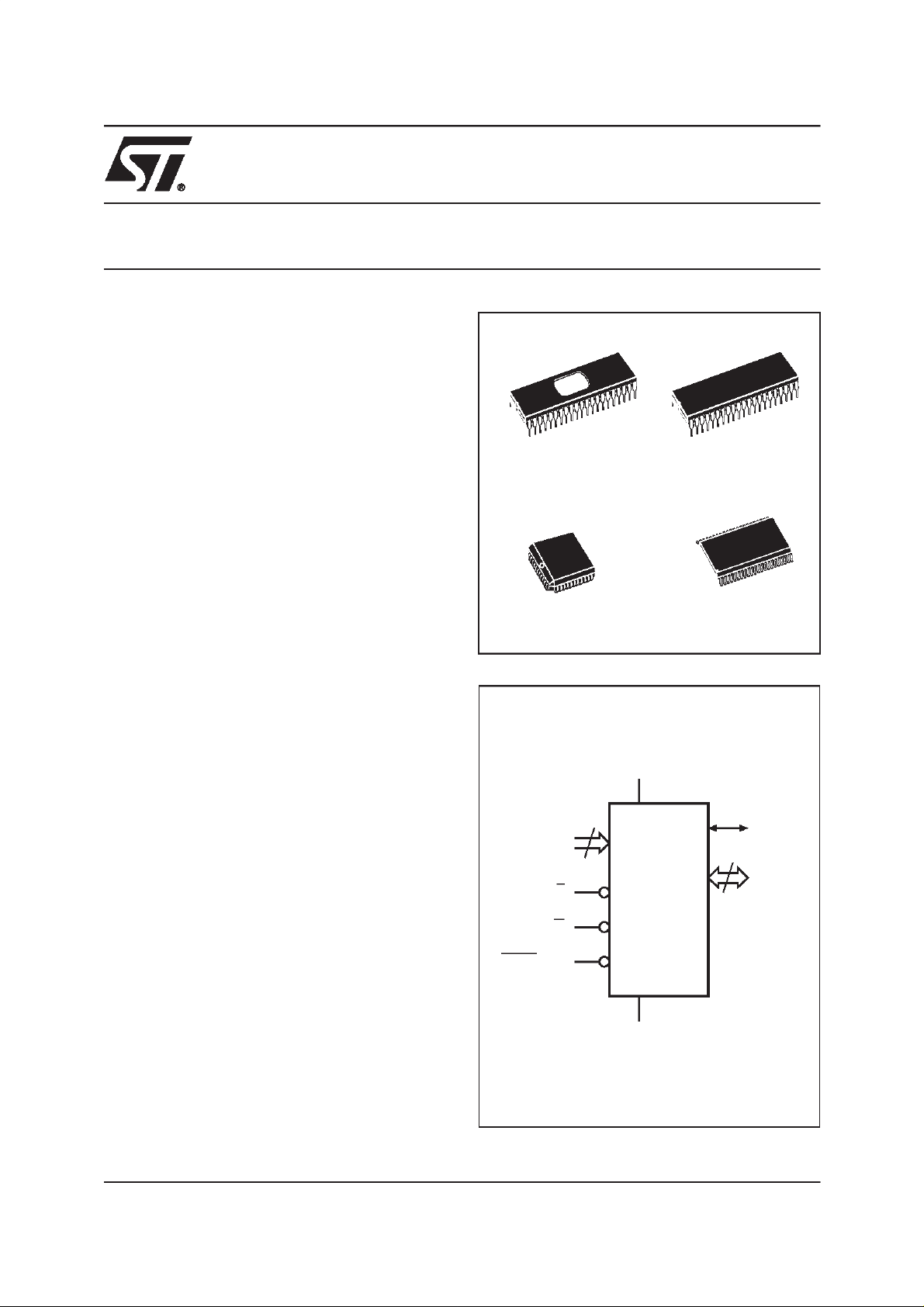
DESCRIPTION
The M27C800 is an 8 Mbit EPROM offered in the
two ranges UV (ultra violet erase) and OTP (one
time programmable). It is ideally suited for microprocessor systems requiringlargedataorprogram
storage. It is organised as either 1 Mwords of 8 bit
or 512 Kwords of 16 bit. The pin-out is compatible
with the most common 8 Mbit Mask ROM.
The FDIP42W (window ceramic frit-seal package)
has a transparent lid which allows the user to expose the chip to ultraviolet lightto erase the bit pattern.
A new patterncanthenbewrittenrapidlytothedevice by following the programming procedure.
For applications where the contentis programmed
only one time and erasure is not required, the
M27C800 is offered in PDIP42, PLCC44 and
SO44 packages.
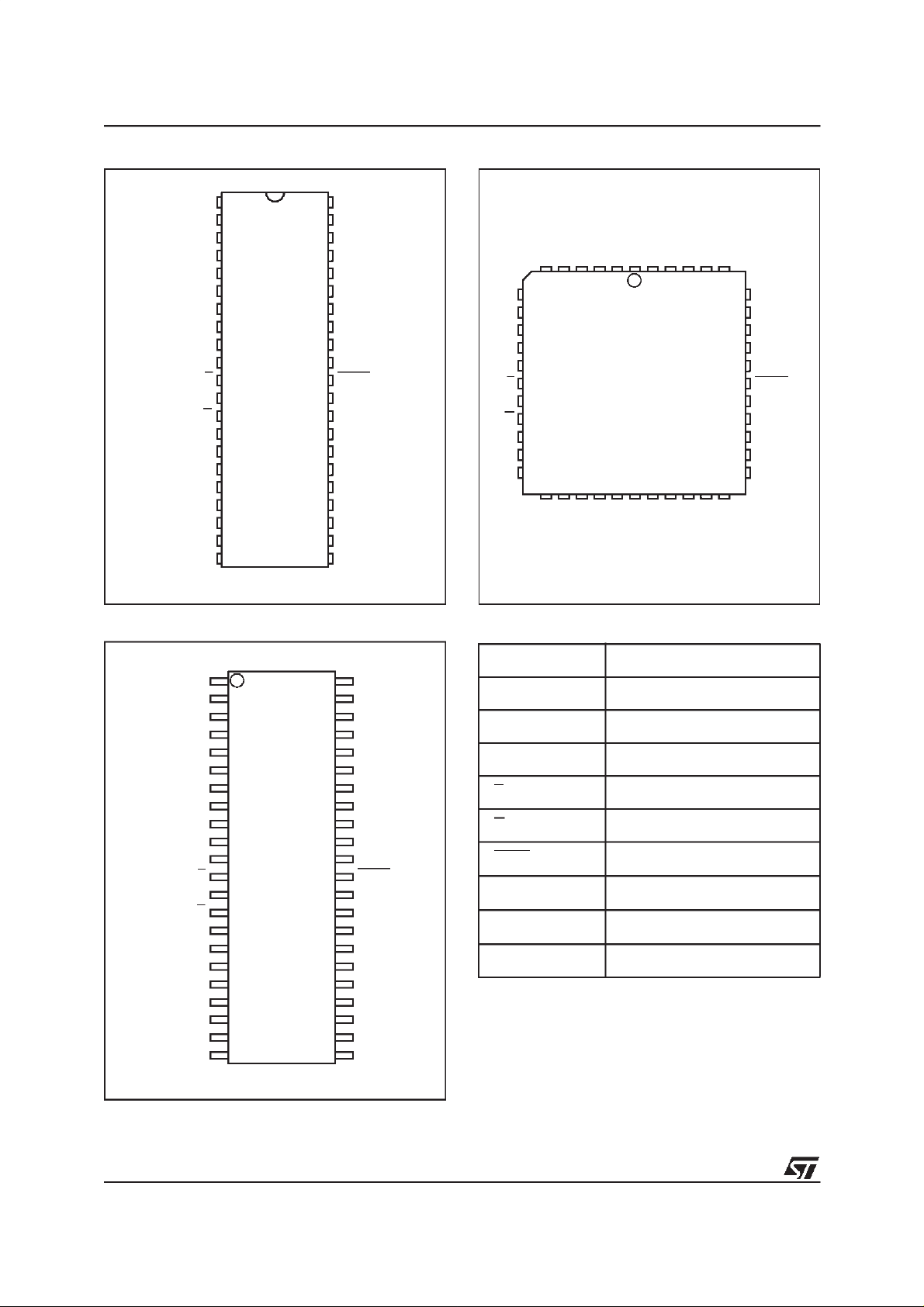
Figure 1. Logic Diagram
V
CC
19
A0-A18
BYTEV
E
G
PP
M27C800
V
SS
Q15A–1
15
Q0-Q14
AI01593
1/17January 2000
M27C800
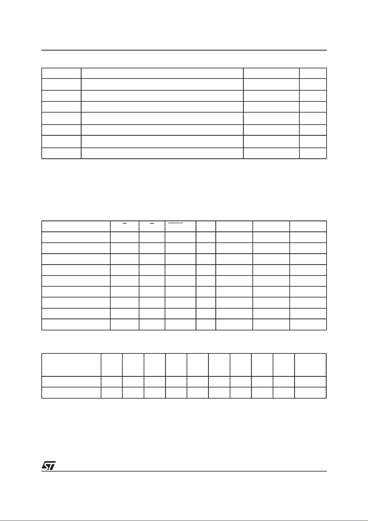
Figure 2A. DIP Connections
1
A18 NC
2
3
A7
A6
4
A5
5
6
A4
7
A3
8
A2
9
A1
10
A0
V
SS
Q0
Q8
Q1
Q9
Q10
Q3
Q11
M27C800
11
E
12
13
G
14
15
16
17
18
19
20
21
42
41
40
39
38
37
36
35
34
33
32
31
30
29
28
27
26
25
24
23
22
AI01594
A8A17
A9
A10
A11
A12
A13
A14
A15
A16
BYTEV
V
SS
Q15A–1
Q7
Q14
Q6
Q13
Q5Q2
Q12
Q4
V
CC
PP
Figure 2B. LCC Connections
SS
A18
A5
A6
A4
A3
A2
A1 A15
A0
E
12
V
SS
Q0
Q8
Q1
Q9
Q2
Q10
V
1
M27C800
23
Q3
NC
Q11
44
V
CC
A17A8NC
A7
Q4
A9
Q12
A10
Q5
A11
34
Q13
A12
A13
A14
A16
BYTEV
V
SS
Q15A–1G
Q7
Q14
Q6
AI02042
PP
Figure 2C. SO Connections
1
NC NC
2
A17 A8
V
Q10
Q11
A7
A6
A5
A4
A3
A2
A1
A0
SS
Q0
Q8
Q9
Q3
3
4
5
6
7
8
9
10
11
M27C800
12
E
13
14
G
15
16
17Q1
18
19
20
21
44
43
42
41
40
39
38
37
36
35
34
33
32
31
30
29
28
27
26
25
24
2322
AI01595
NCA18
A9
A10
A11
A12
A13
A14
A15
A16
BYTEV
V
SS
Q15A–1
Q7
Q14
Q6
Q13
Q5Q2
Q12
Q4
V
CC
PP
Table 1. Signal Names
A0-A18 Address Inputs
Q0-Q7 Data Outputs
Q8-Q14 Data Outputs
Q15A–1 Data Output / Address Input
E Chip Enable
G Output Enable
BYTEV
PP
V
CC
V
SS
NC Not Connected Internally
Byte Mode / Program Supply
Supply Voltage
Ground
2/17
M27C800
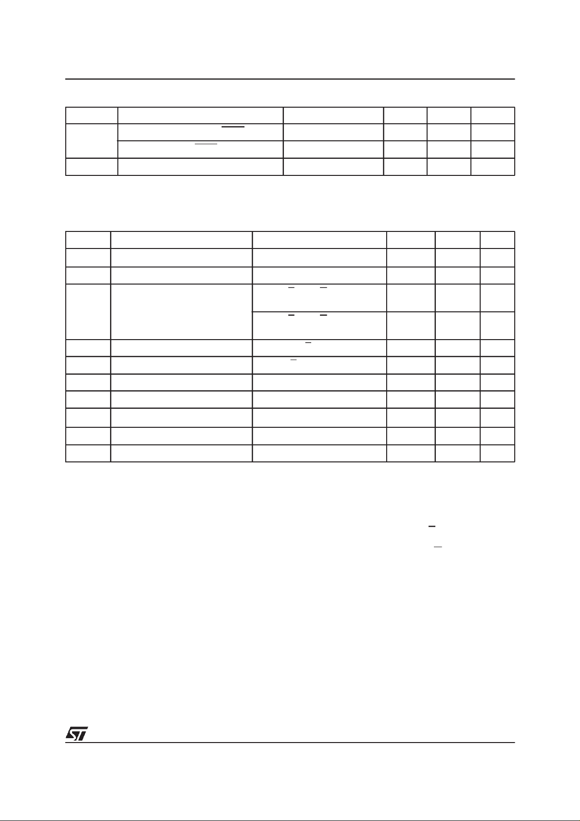
Table 2. Absolute Maximum Ratings
(1)
Symbol Parameter Value Unit
T
A
T
BIAS
T
STG
(2)
V
IO
V
CC
(2)
V
A9
V
PP
Note: 1. Except for the rating ”Operating Temperature Range”, stresses above those listed in the Table ”Absolute Maximum Ratings” may
cause permanent damage to the device. These are stress ratings only and operation of the device at these or anyother conditions
above those indicated in the Operating sections of this specification is not implied. Exposure to Absolute Maximum Rating conditions for extendedperiods may affect device reliability. Referalso to theSTMicroelectronics SURE Program andotherrelevant quality documents.
2. Minimum DC voltage on Input or Output is –0.5V with possible undershoot to –2.0V for a period less than 20ns. Maximum DC
voltage on Output is V
3. Depends on range.
Ambient Operating Temperature
Temperature Under Bias –50 to 125 °C
Storage Temperature –65 to 150 °C
Input or Output Voltage (except A9) –2 to 7 V
Supply Voltage –2 to 7 V
A9 Voltage –2 to 13.5 V
Program Supply Voltage –2 to 14 V
+0.5V with possible overshoot to VCC+2V for a period less than20ns.
CC
(3)
–40 to 125 °C
Table 3. Operating Modes
Mode E G
Read Word-wide
Read Byte-wide Upper V
Read Byte-wide Lower
Output Disable V
Program
V
IL
Verify
Program Inhibit
Standby
Electronic Signature
Note: X = VIHor VIL,VID= 12V ± 0.5V.
V
IL
IL
V
IL
IL
Pulse V
V
IH
V
IH
V
IH
V
IL
V
V
V
V
V
V
V
BYTEV
IL
IL
IL
IH
IH
IL
IH
V
IH
V
IL
V
IL
X X Hi-Z Hi-Z Hi-Z
V
PP
V
PP
V
PP
A9 Q15A–1 Q14-Q8 Q7-Q0
PP
X Data Out Data Out Data Out
XVIHHi-Z Data Out
X
V
IL
Hi-Z Data Out
X Data In Data In Data In
X Data Out Data Out Data Out
X Hi-Z Hi-Z Hi-Z
X X X Hi-Z Hi-Z Hi-Z
IL
V
IH
V
ID
Code Codes Codes
Table 4. Electronic Signature
Identifier A0
Manufacturer’s Code
Device Code
V
IL
V
IH
Q15
and
Q7
Q14
and
Q6
Q13
and
Q5
Q12
and
Q4
Q11
and
Q3
Q10
and
Q2
Q9
and
Q1
Q8
andQ0Hex Data
00100000 20h
10110010 B2h
3/17
M27C800
Table 5. AC Measurement Conditions
High Speed Standard
Input Rise and FallTimes ≤ 10ns ≤ 20ns
Input Pulse Voltages 0 to 3V 0.4V to 2.4V
Input and Output Timing Ref. Voltages 1.5V 0.8V and 2V
Figure 3. AC Testing Input Output Waveform
High Speed
3V
1.5V
0V
Standard
2.4V
0.4V
2.0V
0.8V
AI01822
DEVICE OPERATION
The operatingmodes of the M27C800 are listed in
the OperatingModes Table.A singlepowersupply
is required in the read mode. All inputs are TTL
compatible except for VPPand 12V on A9 for the
Electronic Signature.
Read Mode
The M27C800 has two organisations, Word-wide
and Byte-wide. The organisation is selected by the
signal level on the BYTEVPPpin. When BYTEV
PP
is at VIHthe Word-wide organisation is selected
and the Q15A–1 pin is used for Q15 Data Output.
When theBYTEVPPpin is at VILthe Byte-wide organisation is selected and the Q15A–1 pin is used
for the Address Input A–1. When the memory is
logically regarded as 16 bit wide, but read in the
Byte-wide organisation, then with A–1 at VILthe
Figure 4. AC Testing Load Circuit
1.3V
1N914
3.3kΩ
DEVICE
UNDER
TEST
CL= 30pFfor High Speed
CL= 100pF for Standard
CLincludes JIG capacitance
C
L
OUT
AI01823B
lower 8 bits of the 16 bit data are selected andwith
A–1 at VIHthe upper 8 bits of the 16 bit data are
selected.
The M27C800 has two control functions, both of
which must be logically active in order to obtain
data at the outputs. In addition the Word-wide or
Byte- wide organisation must be selected.
Chip Enable (E) is thepowercontrolandshouldbe
used for device selection. Output Enable (G)is the
output control and should be used to gate data to
the output pins independent of device selection.
Assuming that the addresses are stable, the address access time (t
from E to output (t
ELQV
output after a delay of t
) is equal to the delay
AVQV
). Data is available at the
from the falling edge
GLQV
of G, assuming that E has been low and the addresses have been stable forat least t
AVQV-tGLQV
.
4/17
M27C800
Table 6. Capacitance
(1)
(TA=25°C, f = 1 MHz)
Symbol Parameter Test Condition Min Max Unit
C
IN
C
OUT
Note: 1. Sampled only,not 100% tested.
Input Capacitance (BYTEV
Output Capacitance
)V
PP
Table 7. Read Mode DC Characteristics
Input Capacitance (except BYTEVPP)V
(1)
=0V
IN
= 0V 120 pF
IN
V
=0V
OUT
10 pF
12 pF
(TA= 0 to 70 °C or –40 to 85 °C; VCC=5V±5% or 5V ± 10%; VPP=VCC)
Symbol Parameter Test Condition Min Max Unit
I
I
I
CC
I
CC1
I
CC2
I
V
V
IH
V
V
Note: 1. VCCmust be applied simultaneously with or before VPPand removed simultaneously or after VPP.
Input Leakage Current
LI
Output Leakage Current
LO
0V ≤ V
0V ≤ V
E=V
I
Supply Current
OUT
E=V
I
OUT
Supply Current (Standby) TTL
Supply Current (Standby) CMOS
Program Current
PP
Input Low Voltage –0.3 0.8 V
IL
(2)
Input High Voltage 2
Output Low Voltage
OL
Output High Voltage TTL
OH
2. Maximum DC voltage on Output is V
CC
+ 0.5V.
E>V
I
OH
≤ V
IN
CC
≤ V
OUT
IL
CC
,G=VIL,
= 0mA, f = 8MHz
,G=VIL,
IL
= 0mA, f = 5MHz
E=V
IH
– 0.2V
CC
V
PP=VCC
I
= 2.1mA
OL
= –400µA
2.4 V
±1 µA
±10 µA
70 mA
50 mA
1mA
50 µA
10 µA
V
+1
CC
0.4 V
V
Standby Mode
The M27C800 has astandbymode which reduces
the supply current from 50mA to 100µA. The
M27C800 is placedin the standby mode by applying aCMOS high signal to the Einput. When in the
standby mode, the outputs are in a high impedance state, independent of the G input.
5/17
M27C800
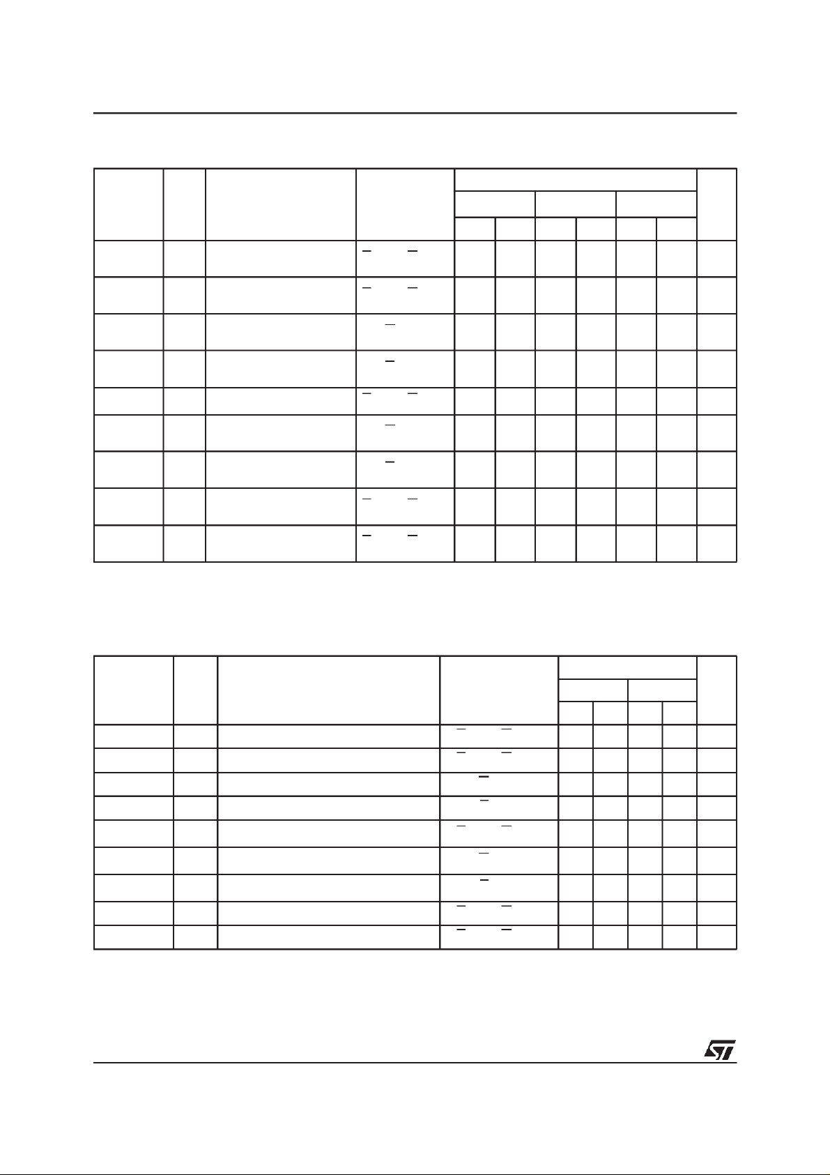
Table 8A. Read Mode AC Characteristics
(1)
(TA= 0 to 70 °C or –40 to 85 °C; VCC=5V±5% or 5V ± 10%; VPP=VCC)
M27C800
Symbol Alt Parameter TestCondition
t
AVQV
t
BHQV
t
ELQV
t
GLQV
(2)
t
BLQZ
(2)
t
EHQZ
(2)
t
GHQZ
t
AXQX
t
BLQX
Note: 1. VCCmust be applied simultaneously with or before VPPand removed simultaneously or after V
2. Sampled only,not 100% tested.
3. Speed obtained with High Speed AC measurement conditions.
Address Validto Output
t
ACC
Valid
BYTE High to Output
t
ST
Valid
Chip Enable Low to
t
CE
Output Valid
Output Enable Low to
t
OE
Output Valid
t
BYTE Low to Output Hi-Z
STD
Chip Enable High to
t
DF
Output Hi-Z
Output Enable High to
t
DF
Output Hi-Z
Address Transition to
t
OH
Output Transition
BYTE Low to Output
t
OH
Transition
E=V
E=V
E=V
E=V
E=V
,G=V
IL
,G=V
IL
G=V
E=V
,G=V
IL
G=V
E=V
,G=V
IL
,G=V
IL
IL
IL
IL
IL
IL
IL
IL
IL
IL
(3)
-50
Min Max Min Max Min Max
50 70 90 ns
50 70 90 ns
50 70 90 ns
30 35 45 ns
30 30 30 ns
030030030ns
030030030ns
555ns
555ns
-70 -90
PP.
Unit
Table 8B. Read Mode AC Characteristics
(1)
(TA= 0 to 70 °C or –40 to 85 °C; VCC=5V±5% or 5V ± 10%; VPP=VCC)
Symbol Alt Parameter Test Condition
t
t
AVQV
t
BHQV
t
ELQV
t
GLQV
(2)
t
BLQZ
(2)
t
EHQZ
(2)
t
GHQZ
t
AXQX
t
BLQX
Note: 1. VCCmust be applied simultaneously with or before VPPand removed simultaneously or after V
2. Sampled only,not 100% tested.
Address Valid to Output Valid E= VIL,G=V
ACC
t
BYTE High to Output Valid
ST
t
Chip Enable Low to Output Valid
CE
t
Output Enable Low to Output Valid
OE
t
BYTE Low to Output Hi-Z
STD
t
Chip Enable High to Output Hi-Z
DF
t
Output Enable High to Output Hi-Z
DF
t
Address Transitionto Output Transition E = VIL,G=V
OH
t
BYTE Low to Output Transition
OH
E=V
E=V
E=V
,G=V
IL
G=V
E=V
,G=V
IL
G=V
E=V
,G=V
IL
IL
IL
IL
IL
IL
IL
IL
IL
IL
M27C800
Unit-100 -120/150
Min Max Min Max
100 120 ns
100 120 ns
100 120 ns
50 60 ns
40 50 ns
0 40 0 50 ns
0 40 0 50 ns
55ns
55ns
PP.
6/17
 Loading...