

SGS Thomson Microelectronics M27C516 Datasheet
5V ± 10% SUPPLYVOLTAGEin READ
OPERATION
FASTACCESSTIME: 35ns
LOW POWERCONSUMPTION:
– ActiveCurrent 30mAat 5MHz
– Stand-byCurrent 100µA
PROGRAMMINGVOLTAGE:12.75V±0.25V
PROGRAMMINGTIME: 100µs/word (typical)
ELECTRONICSIGNATURE
– ManufacturerCode:0020h
– DeviceCode: 000Fh
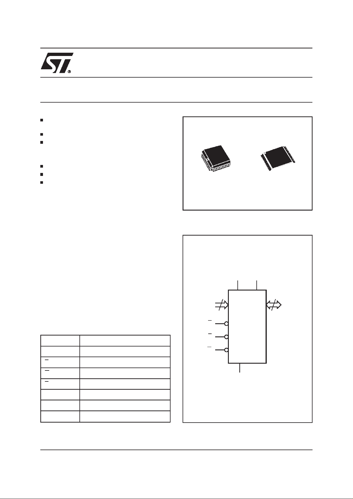
DESCRIPTION
TheM27C516 is a 512Kbit EPROM offeredin the
OTP range (one time programmable). It is ideally
suited for microprocessorsystems requiring large
data or program storage and is organized as
32,768 words of 16 bits.
TheM27C516isofferedin aPLCC44andTSOP40
(10 x 14mm)packages.
M27C516
512 Kbit (32Kb x16) OTP EPROM
PLCC44 (C) TSOP40 (N)
Figure1. LogicDiagram
V
CC
15
A0-A14
V
PP
10 x 14mm
16
Q0-Q15
P
Table1. SignalNames
A0-A14 Address Inputs
Q0-Q15 Data Outputs
E Chip Enable
G Output Enable
P Program Enable
V
CC
V
PP
V
SS
September 1998 1/12
Supply Voltage
Program Supply
Ground
E
G
M27C516
V
SS
AI00932
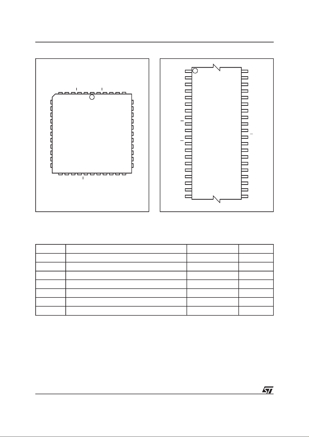
M27C516
Figure2A. LCC Pin Connections
Q13
Q14
Q15
CC
NC
VPPE
V
1
44
Q12
Q11
Q10
Q9 A10
Q8
V
SS
12
M27C516
NC
Q6
Q5
Q4
23
G
Q3
Q2
Q1
Q0
NC
A0
P
A1
NC
A2
NC
A3
A14
34
A4
A13
A12
A11
A9
V
SS
NC
A8Q7
A7
A6
A5
AI00934
Figure2B. TSOPPin Connections
A9
A10
A11
A12 A6
A13 A5
A14
NC
NC
V
CC
V
PP
DQ15
DQ14
DQ13
DQ12 DQ4
DQ11 DQ5
DQ10
DQ9
DQ8
1
P
M27C516
10
(Normal)
11
E
20 21
40
31
30
AI01600
V
SS
A8
A7
A4
A3
A2
A1
A0
G
DQ0
DQ1
DQ2
DQ3
DQ6
DQ7
V
SS
Warning: NC = Not Connected.
Table2. AbsoluteMaximum Ratings
(1)
Warning: NC = Not Connected.
Symbol Parameter Value Unit
T
A
T
BIAS
T
STG
(2)
V
IO
V
CC
(2)
V
A9
V
PP
Notes:
1. Except for therating ”Operating Temperature Range”, stresses above those listedin the Table ”AbsoluteMaximum Ratings”
may cause permanent damage to the device. These are stress ratings only and operation of the device at these or any other
conditions above those indicated in the Operatingsections of this specification is not implied.Exposure to Absolute Maximum
Rating conditions for extendedperiods may affectdevice reliability.Refer also to the STMicroelectronicsSURE Program and other
relevant quality documents.
2. Minimum DC voltage on Input or Output is –0.5V with possible undershoot to –2.0V for a period less than 20ns. Maximum DC
voltage on Output is V
3. Depends on range.
Ambient OperatingTemperature
TemperatureUnder Bias –50 to 125 °C
Storage Temperature –65 to 150
Input or Output Voltages (except A9) –2 to 7 V
Supply Voltage –2 to 7 V
A9 Voltage –2 to 13.5 V
Program SupplyVoltage –2 to 14 V
+0.5Vwith possible overshoot to VCC+2V for a period less than20ns.
CC
(3)
–40 to 125
C
°
C
°
2/12
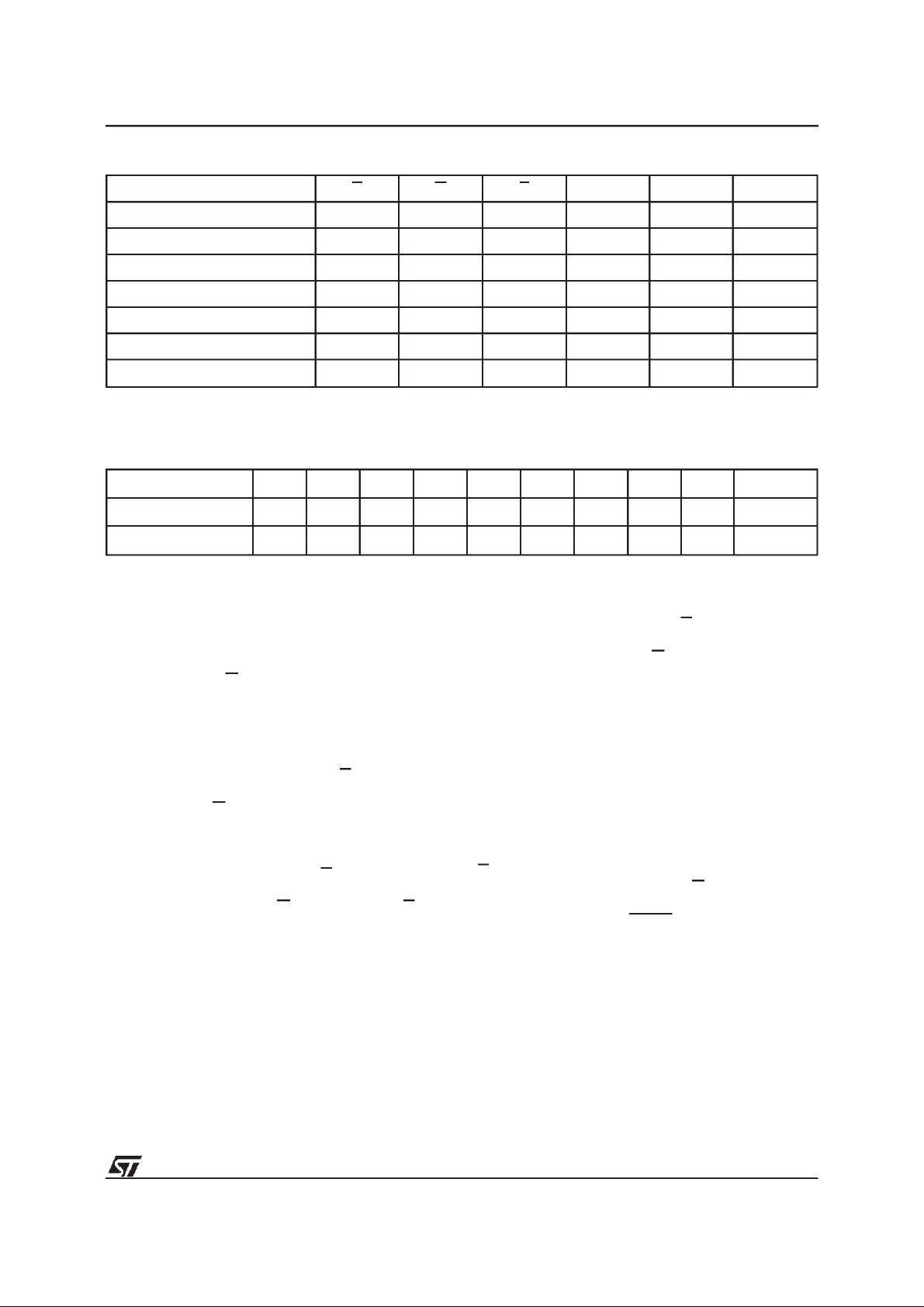
Table3. OperatingModes
M27C516
Mode E G P A9 V
Read V
Output Disable V
Program V
Verify V
Program Inhibit V
Standby V
Electronic Signature V
Notes
or VIL,VID=12V±0.5V
:X=V
IH
IL
IL
IL
IL
IH
IH
IL
V
IL
V
IH
XV
V
IL
XXXVPPHi-Z
XXXVCCHi-Z
V
IL
V
IH
XXVCCHi-Z
Pulse X V
IL
V
IH
V
IH
XVCCData Out
XVPPData Out
V
ID
PP
PP
V
CC
Table4. ElectronicSignature
Identifier A0 Q7 Q6 Q5 Q4 Q3 Q2 Q1 Q0 Hex Data
Manufacturer’s Code V
Device Code V
Note: OutputsQ8-Q15 are set to ’0’.
IL
IH
DEVICEOPERATION
Theoperating modesof theM27C516are listed in
the Operating Modes table.A single power supply
is required in the read mode. All inputs are TTL
levels except for G and 12V on A9 for Electronic
Signature.
ReadMode
The M27C516 has two control functions, both of
which must be logically active in order to obtain
data at the outputs.Chip Enable (E) is the power
control and should be used for device selection.
OutputEnable(G) isthe outputcontrol and should
be used to gate data to the output pins, independent of device selection. Assuming that the
addresses are stable, the address access time
)isequaltothedelayfromE tooutput(t
(t
AVQV
Datais availableatthe outputaftera delayof t
from the falling edge of G, assuming that E has
been low and the addresses have been stablefor
at least t
AVQV-tGLQV
.
StandbyMode
TheM27C516has a standby mode which reduces
00100000 20h
00001111 0Fh
M27C516is placed in the standbymode by applyinga CMOShigh signalto theE input.When in the
standbymode, theoutputsareina highimpedance
state,independentof theG input.
Two Line Output Control
BecauseOTP EPROMsare usually used in larger
memoryarrays,theproductfeaturesa 2linecontrol
functionwhich accommodatesthe use of multiple
memory connection. The two line control function
allows:
a. thelowestpossiblememorypowerdissipation,
b. completeassurance that output bus contention
will not occur.
Forthemostefficientuse ofthesetwo controllines,
ELQV
GLQV
deviceselectingfunction, whileG shouldbe made
a common connection to all devices in the array
E should be decoded and used as the primary
).
and connected to the READ line from the system
controlbus. This ensuresthat all deselectedmemory devices are in their low power standby mode
and that the output pins areonly activewhen data
is requiredfrom a particular memory device.
the supply current from 30mA to 100µA. The
Q0 - Q15
Data In
Codes
3/12
M27C516
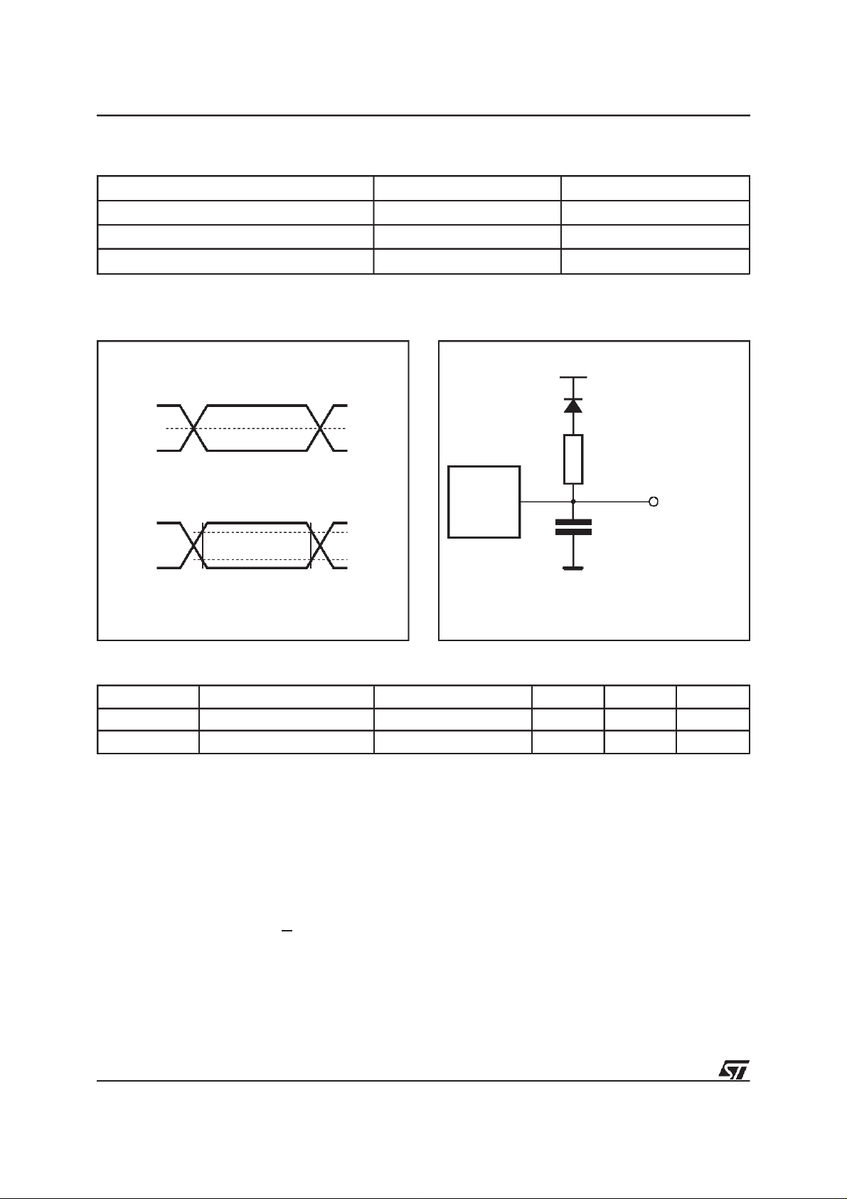
Table5. AC MeasurementConditions
High Speed Standard
Input Rise and Fall Times ≤ 10ns ≤ 20ns (10% to 90%)
Input Pulse Voltages 0 to 3V 0.4V to 2.4V
Input and Output Timing Ref. Voltages 1.5V 0.8V and 2V
Figure3. ACTestingInput Output Waveform
High Speed
3V
1.5V
0V
Standard
2.4V
0.4V
Table 6. Capacitance
Symbol Parameter Test Condition Min Max Unit
C
IN
C
OUT
Notes. 1. VCCmust be applied simultaneously with or before VPPandremoved simultaneouslywith or after VPP.
2. This parameter is sampled only and not tested 100%.
Input Capacitance VIN=0V 6 pF
Output Capacitance V
=25°C, f =1 MHz)
(T
A
2.0V
0.8V
AI01822
Figure 4. AC TestingLoad Circuit
1.3V
1N914
3.3kΩ
DEVICE
UNDER
TEST
CL= 30pF or 60pF or 100pF
CLincludes JIG capacitance
=0V 12 pF
OUT
OUT
AI02024B
SystemConsiderations
The power switching characteristics of Advanced
CMOS EPROMsrequire careful decouplingof the
devices. The supply current, I
, has three seg-
CC
ments that are of interest to the system designer:
the standby current level, the active current level,
and transientcurrent peaks that are produced by
the falling and risingedges ofE. Themagnitudeof
the transient current peaks is dependent on the
capacitiveandinductiveloadingof thedeviceatthe
output.Theassociatedtransientvoltagepeakscan
be suppressed by complying with the two line
4/12
outputcontroland by properlyselecteddecoupling
capacitors.It is recommendedthat a 1µF ceramic
capacitor be used on every device between V
CC
andVSS. Thisshouldbe a highfrequencycapacitor
of low inherent inductanceand should be placed
as close to the device as possible. In addition, a
4.7µF bulk electrolytic capacitor should be used
betweenV
andVSSforevery eight devices.The
CC
bulk capacitor should be located near the power
supplyconnection point.The purpose of the bulk
capacitor is to overcomethe voltage drop caused
by the inductiveeffectsof PCBtraces.
 Loading...