

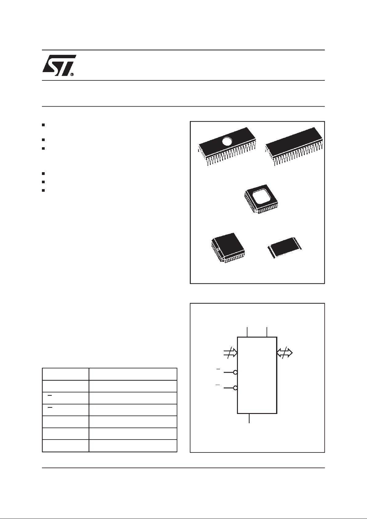
4 Mbit (256Kb x16) UV EPROM and OTP EPROM
5V ± 10% SUPPLYVOLTAGEin READ
OPERATION
FASTACCESSTIME: 45ns
LOW POWERCONSUMPTION:
– ActiveCurrent 70mAat 10MHz
– StandbyCurrent 100µA
PROGRAMMINGVOLTAGE:12.75V ± 0.25V
PROGRAMMINGTIME: 100µs/byte(typical)
ELECTRONICSIGNATURE
– ManufacturerCode: 0020h
– DeviceCode: 0044h
DESCRIPTION
The M27C4002 is a 4 Mbit EPROM offered in the
two ranges UV (ultra violet erase) and OTP (one
time programmable). It is ideally suited for microprocessorsystemsrequiringlargeprogramsandis
organisedas 262,144words of 16 bits.
The FDIP40W(window ceramicfrit-seal package)
and the JLCC44W (J-lead chip carrierpackages)
have transparent lids which allow the user to expose the chip to ultraviolet light to erase the bit
pattern. A new pattern can then be written to the
deviceby followingthe programmingprocedure.
Forapplicationswherethe contentisprogrammed
only one time and erasure is not required, the
M27C4002 is offered in PDIP40, PLCC44 and
TSOP40(10 x 20 mm) packages.
Table1. SignalNames
A0-A17 Address Inputs
M27C4002
40
1
FDIP40W (F)
PLCC44 (C)
Figure1. LogicDiagram
V
18
A0-A17 Q0-Q15
E
40
JLCC44W (J)
V
CC
M27C4002
PP
1
PDIP40 (B)
TSOP40 (N)
10 x 20 mm
16
Q0-Q15 Data Outputs
E Chip Enable
G Output Enable
V
PP
V
CC
V
SS
September 1998 1/16
Program Supply
Supply Voltage
Ground
G
V
SS
AI00727B
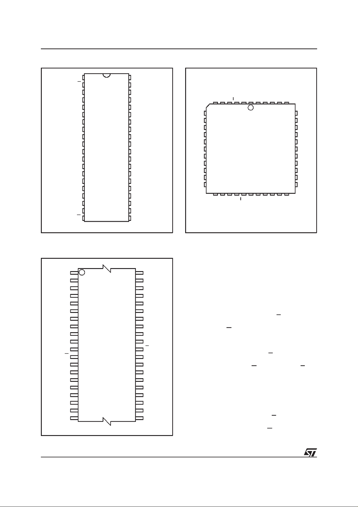
M27C4002
Figure2A. DIP Pin Connections
V
PP
Q15
Q14
Q13
Q12
Q11
Q10
Q9
Q8
V
SS
Q7
Q6
Q5
Q4
Q3
Q2
Q0
1
2
3
4
5
6
7
8
9
10
M27C4002
11
12
13
14
15
16
17
18
19
40
39
38
37
36
35
34
33
32
31
30
29
28
27
26
25
24
23
22
2120
AI00728
V
CC
A17E
A16
A15
A14
A13
A12
A11
A10
A9
V
SS
A8
A7
A6
A5
A4
A3
A2Q1
A1
A0G
Figure2B. LCC Pin Connections
Q15
Q13
Q14
Q12
Q11
Q10
Q9 A10
Q8
V
12
SS
NC
Q6
Q5
Q4
Q3
Warning: NC = Not Connected.
Q2
M27C4002
Q1
Q0
CC
NC
VPPE
V
1
44
23
G
A0
NC
A17
A1
A16
A2
A15
A3
A14
34
A4
A13
A12
A11
A9
V
SS
NC
A8Q7
A7
A6
A5
AI00729
Figure2C. TSOP Pin Connections
A9
A10
A11
A12 A6
A13 A5
A14
A15
A16
A17
V
CC
V
PP
DQ15
DQ14
DQ13
DQ12 DQ4
DQ11 DQ5
DQ10
DQ9
DQ8
1
M27C4002
10
(Normal)
11
E
20 21
40
31
30
AI01831
V
SS
A8
A7
A4
A3
A2
A1
A0
G
DQ0
DQ1
DQ2
DQ3
DQ6
DQ7
V
SS
DEVICEOPERATION
The operating modesof the M27C4002are listed
in the OperatingModes table. A single power supplyis requiredin thereadmode. Allinputs are TTL
levels except for V
and 12V on A9for Electronic
pp
Signature.
Read Mode
The M27C4002 has two control functions,both of
which must be logically active in order to obtain
data at the outputs. Chip Enable (E) is the power
control and should be used for device selection.
OutputEnable(G) is the outputcontrol and should
be used to gate data to the output pins, independent of device selection. Assuming that the
addresses are stable, the address access time
)isequalto thedelayfrom Etooutput(t
(t
AVQV
Datais availableat theoutputaftera delayof t
ELQV
GLQV
from the falling edge of G, assuming that E has
been low andthe addresseshave beenstable for
at least t
AVQV-tGLQV
.
StandbyMode
The M27C4002 has a standby mode which reducesthesupplycurrentfrom50mAto100µA.The
M27C4002 is placed in the standby mode by applyinga CMOShigh signalto theE input. Whenin
thestandbymode,theoutputsare in a highimpedance state,independentof theG input.
).
2/16
M27C4002
Table2. Absolute MaximumRatings
(1)
Symbol Parameter Value Unit
T
A
T
BIAS
T
STG
V
IO
V
CC
V
A9
V
PP
Notes: 1. Except for the rating ”Operating Temperature Range”, stresses above those listed in theTable ”AbsoluteMaximum Ratings”
2. Minimum DC voltage on Input or Output is –0.5V with possible undershoot to –2.0V for a period less than 20ns. Maximum DC
3. Depends on range.
Ambient Operating Temperature
Temperature Under Bias –50 to125
Storage Temperature –65 to150
(2)
Input or Output Voltages (except A9) –2 to7 V
Supply Voltage –2 to7 V
(2)
A9 Voltage –2 to13.5 V
Program Supply Voltage –2 to14 V
may cause permanentdamage to thedevice. Theseare stress ratings only and operation of the device at these or any other
conditions above those indicated in the Operatingsections of this specification is not implied.Exposure to Absolute Maximum
Rating conditions for extendedperiods may affectdevice reliability.Refer also to the STMicroelectronicsSURE Programand other
relevant quality documents.
voltage on Output is V
+0.5Vwith possible overshoot to VCC+2V for a period less than20ns.
CC
(3)
–40 to125
C
°
C
°
C
°
Table3. OperatingModes
Mode E G A9 V
Read V
Output Disable V
Program V
Verify V
Program Inhibit V
Standby V
Electronic Signature V
Note:X =VIHor VIL,VID= 12V ± 0.5V
IL
IL
Pulse V
IL
IH
IH
IH
IL
PP
V
IL
V
IH
IH
V
IL
V
IH
XXV
V
IL
XV
XV
CC
CC
or V
or V
SS
SS
XVPPData In
XVPPData Out
XVPPHi-Z
or V
CC
SS
V
ID
V
CC
Q0 - Q15
Data Out
Hi-Z
Hi-Z
Codes
Table4. ElectronicSignature
Identifier A0 Q7 Q6 Q5 Q4 Q3 Q2 Q1 Q0 Hex Data
Manufacturer’s Code V
Device Code V
Note: Outputs Q8-Q15 areset to ’0’.
IL
IH
00100000 20h
01000100 44h
Two Line Output Control
BecauseEPROMsareusuallyusedinlargermemory arrays, the product features a 2 line control
functionwhich accommodatesthe use of multiple
memory connection. The two line control function
allows:
a. the lowest possible memory power dissipation,
b. complete assurancethat output bus contention
will not occur.
Forthemostefficientuse ofthesetwocontrollines,
E should be decoded and used as the primary
deviceselectingfunction,while G shouldbe made
a common connection to all devices in the array
and connected to the READ line from the system
controlbus. This ensuresthat all deselectedmemory devices are in their low power standby mode
and that the output pins areonly active when data
is requiredfrom a particular memory device.
3/16
M27C4002
Table5. AC MeasurementConditions
High Speed Standard
Input Rise and Fall Times
Input Pulse Voltages 0 to 3V 0.4Vto 2.4V
Input and Output Timing Ref. Voltages 1.5V 0.8V and 2V
Figure3. ACTestingInput Output Waveform
High Speed
3V
1.5V
0V
Standard
2.4V
0.4V
2.0V
0.8V
AI01822
10ns
≤
Figure4. ACTestingLoad Circuit
1.3V
1N914
3.3kΩ
DEVICE
UNDER
TEST
C
CL= 30pF for High Speed
CL= 100pF for Standard
CLincludes JIG capacitance
L
≤
20ns
OUT
AI01823B
Table6. Capacitance
Symbol Parameter Test Condition Min Max Unit
C
IN
C
OUT
Note: 1. Sampled only,not 100% tested.
SystemConsiderations
The power switching characteristicsof Advanced
CMOS EPROMsrequire careful decoupling of the
devices. The supply current, I
ments that are of interest to the system designer:
the standby currentlevel, the active current level,
and transientcurrent peaks that are produced by
thefalling and rising edgesof E. Themagnitudeof
the transient current peaks is dependent on the
output capacitive and inductiveloading of the device.
(1)
(TA=25°C, f = 1MHz )
Input Capacitance VIN=0V 6 pF
Output Capacitance V
=0V 12 pF
OUT
control and by properly selected decoupling capacitors. Itis recommendedthat a 0.1µF ceramic
capacitor be used on every device between V
, has three seg-
CC
andVSS. Thisshouldbea highfrequencycapacitor
of low inherent inductance and should be placed
as close to the device as possible. In addition, a
4.7µF bulk electrolytic capacitor should be used
betweenV
andVSSfor everyeight devices. The
CC
bulk capacitor should be located near the power
supply connection point.The purpose of the bulk
capacitoris to overcome the voltage drop caused
by the inductive effectsof PCBtraces.
The associated transient voltage peaks can be
suppressed by complying with the two line output
4/16
CC
M27C4002
Table7. Read Mode DC Characteristics
(1)
(TA=0 to 70 °C or –40 to 85 °C;VCC=5V±5% or 5V± 10%;VPP=VCC)
Symbol Parameter Test Condition Min Max Unit
I
LI
I
LO
I
CC
I
CC1
I
CC2
I
PP
V
IL
V
IH
V
OL
V
OH
Notes: 1. VCCmust be applied simultaneously with or before VPPand removed simultaneously or after V
2. Maximum DC voltage on Output is VCC+0.5V.
Input Leakage Current 0V ≤ VIN≤ V
Output LeakageCurrent 0V≤V
E=V
= 0mA, f = 10MHz
I
Supply Current
OUT
E=V
I
= 0mA, f = 5MHz
OUT
Supply Current (Standby)TTL E = V
≤
OUT
,G=VIL,
IL
,G=VIL,
IL
IH
CC
V
CC
Supply Current (Standby)CMOS E > VCC–0.2V 100
Program Current VPP=V
CC
Input Low Voltage –0.3 0.8 V
(2)
Input High Voltage 2 VCC+1 V
Output LowVoltage IOL= 2.1mA 0.4 V
Output HighVoltageTTL IOH= –400µA 2.4 V
Output High Voltage CMOS I
= –100µAV
OH
CC
– 0.7V V
PP.
±10 µA
10
±
70 mA
50 mA
1mA
10 µA
A
µ
A
µ
Table8A. Read ModeAC Characteristics
(1)
(TA=0 to 70 °C or –40 to 85 °C;VCC=5V±5% or 5V± 10%;VPP=VCC)
Symbol Alt Parameter
Test
Condition
-45
(3)
Min Max Min Max Min Max Min Max
t
AVQV
t
ELQV
t
GLQV
(2)
t
EHQZ
(2)
t
GHQZ
t
AXQX
Notes: 1. VCCmust be applied simultaneously with or before VPPand removed simultaneously or after V
2. Sampled only, not 100% tested.
3. In case of 70ns speed see High Speed AC Measurement conditions.
Address Valid to
t
ACC
Output Valid
Chip Enable Low
t
CE
to Output Valid
Output Enable
t
OE
Low to Output Valid
Chip Enable High
t
DF
to Output Hi-Z
Output Enable
t
DF
High to Output Hi-Z
Address Transition
t
OH
to Output Transition
E=VIL,
G=V
G=V
E=V
G=V
E=V
E=VIL,
G=V
IL
IL
IL
IL
IL
IL
45 60 80 90 ns
45 60 80 90 ns
25 30 40 40 ns
0 30 0 30 0 30 0 30 ns
0 30 0 30 0 30 0 30 ns
0000ns
-60
(3)
M27C4002
-80 -90
PP.
Unit
5/16
 Loading...