

SGS Thomson Microelectronics M24C04-DW6T, M24C04-BN6, M24C04, M24C02-W, M24C02-RMN6T Datasheet
...
1/20May 2000
M24C16, M24C08
M24C04, M24C02, M24C01
16/8/4/2/1 Kbit Serial I²C Bus EEPROM
■ Two Wire I
2
C Serial Interface
Supports 400 kHz Protocol
■ Single Supply Voltage:
– 4.5V to 5.5V for M24Cxx
– 2.5V to 5.5V for M24Cxx-W
– 1.8V to 3.6V for M24Cxx-R
■ Hardware Write Control
■ BYTE and PAGE WRITE (up to 16 Bytes)
■ RANDOM and SEQUENTIAL READ Modes
■ Self-Tim ed P ro g ra m ming Cycle
■ Automatic Address Incrementing
■ Enhanced ESD/Latch-Up Behavior
■ 1 Million Erase/Write Cycles (minimum)
■ 40 Year Data Retention (minimum)
DESCRIPTION
These I
2
C-compatible electrically erasable
programmable memory (EEPROM) devices are
organized as 2048/1024/512/256/128 x 8 bit
(M24C16, M24C08, M24C04, M24C02, M24C01),
and operate with a power supply down to 2.5 V (for
the -W version of each device), and down to 1.8 V
(for the -R version of each device).
The M24C16, M24C08, M24C04, M24C02,
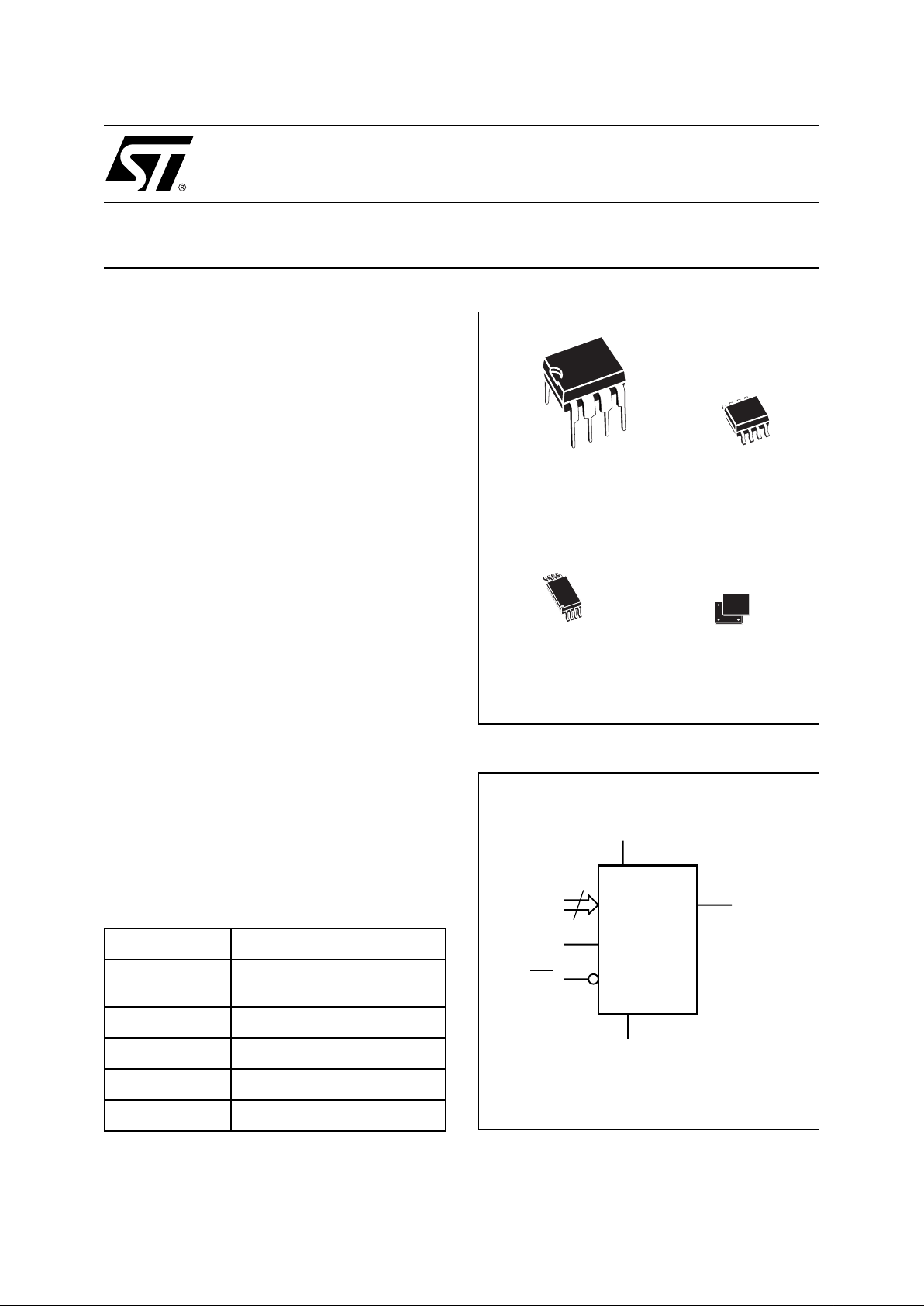
M24C01 are available in Plastic Dual-in-Line,
Plastic Small Outline and Thin Shrink Small
Outline packages. The M24C16-R is also
available in a chip-scale (SBGA) package.
Figure 1. Logic Diagram
AI02033
3
E0-E2 SDA
V
CC
M24Cxx
WC
SCL
V
SS
Table 1. Signal Names
E0, E1, E2 Chip Enable Inputs
SDA Serial Data/Address Input/
Output
SCL Serial Clock
WC Write Control
V
CC
Supply Voltage
V
SS
Ground
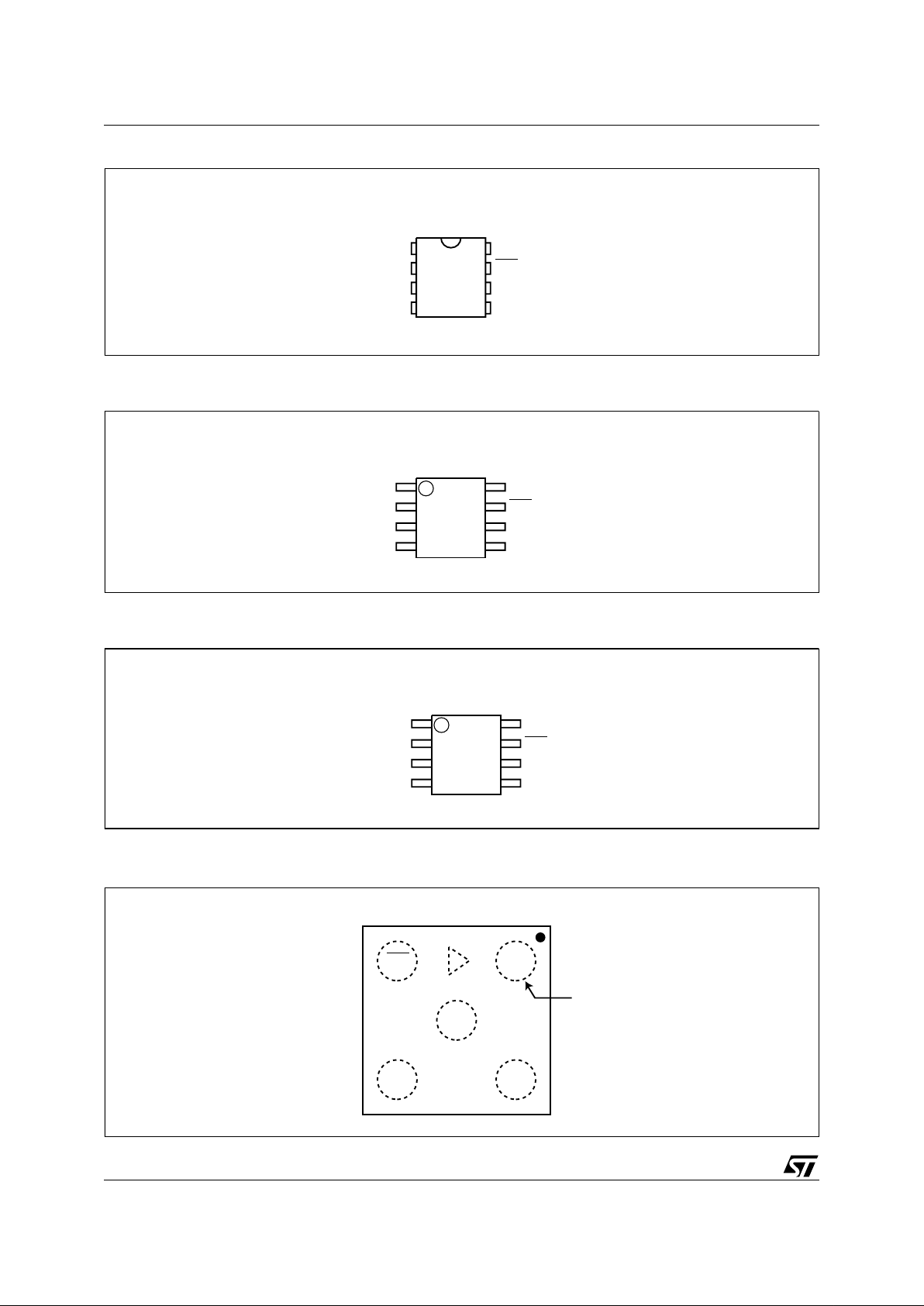
PSDIP8 (BN)
0.25 mm frame
SO8 (MN)
150 mil width
TSSOP8 (DW)
169 mil width
8
1
8
1
8
1
SBGA
SBGA5 (EA)
75 mil width
M24C16, M24C08, M24C04, M24C02, M24C01
2/20
Figure 2A. DIP Connections
Note: 1. NC = Not Connected
Figure 2B. SO Connections
Note: 1. NC = Not Connected
Figure 2C. Standard-TSSOP Connections
Note: 1. NC = Not Connected
SDAV
SS
SCL
WC
V
CC
/ E2
AI02034D
M24Cxx
1
2
3
4
8
7
6
5
/ E2/ E2/ E2NC
/ E1
/ E1/ E1/ NCNC
/ E0
/ E0/ NC/ NCNC
/1Kb
/2Kb/4Kb/8Kb16Kb
1
AI02035D
2
3
4
8
7
6
5
SDAV
SS
SCL
WC
V
CC
/ E2
M24Cxx
/ E2/ E2/ E2NC
/ E1
/ E1/ E1/ NCNC
/ E0
/ E0/ NC/ NCNC
/1Kb
/2Kb/4Kb/8Kb16Kb
1
AI02036D
2
3
4
8
7
6
5
SDAV
SS
SCL
WC
V
CC
/ E2
M24Cxx
/ E2/ E2/ E2NC
/ E1
/ E1/ E1/ NCNC
/ E0
/ E0/ NC/ NCNC
/1Kb
/2Kb/4Kb/8Kb16Kb
Figure 2D. SBGA Connections (top view, marking side, with balls on the underside)
AI02796E
SCL V
SS
SDA
WC V
CC
M24C16
Ball "1"
3/20
M24C16, M24C08, M24C04, M24C 02, M24C01
These memory devices are compatible with the
I
2
C memory standard. This is a two wire serial
interface that uses a bi-directional data bus and
serial clock. The memory carries a built-in 4-bit
unique Device Type Identifier code (1010) in
accordance with the I
2
C bus definition.
The memory behaves as a slave device in the I
2
C
protocol, with all memory operations synchronized
by the serial clock. Read and Write operations are
initiated by a START condition, gene rated by the
bus master. The START condition is followed by a
Device Select Code and RW
bit (as described in
Table 3), terminated by an acknowledge bit.
When writing data to the memory, the memory
inserts an acknowledge bit during the 9
th
bit time,
following the bus master’s 8-bit transmission.
When data is read by the bus master, the bus
master acknowledges the receipt of the data b yte
in the same way. Data transfers are terminated by
a STOP condition after an Ack for WRITE, and
after a NoAck for READ.
Power On Reset: V
CC
Lock-Out Write Protect
In order to prevent data corruption and inadvertent
write operations during power up, a Power On
Reset (POR) circuit is included. The internal reset
is held active until the V
CC
voltage has reached
the POR threshold value, and all operations are
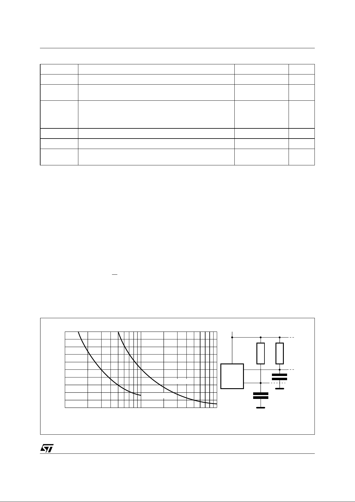
Figure 3. Maximum R
L
Value versus Bus Capacitance (C
BUS
) for an I2C Bus
AI01665
V
CC
C
BUS
SDA
R
L
MASTER
R
L
SCL
C
BUS
100
0
4
8
12
16
20
C
BUS
(pF)
Maximum RP value (kΩ)
10 1000
fc = 400kHz
fc = 100kHz
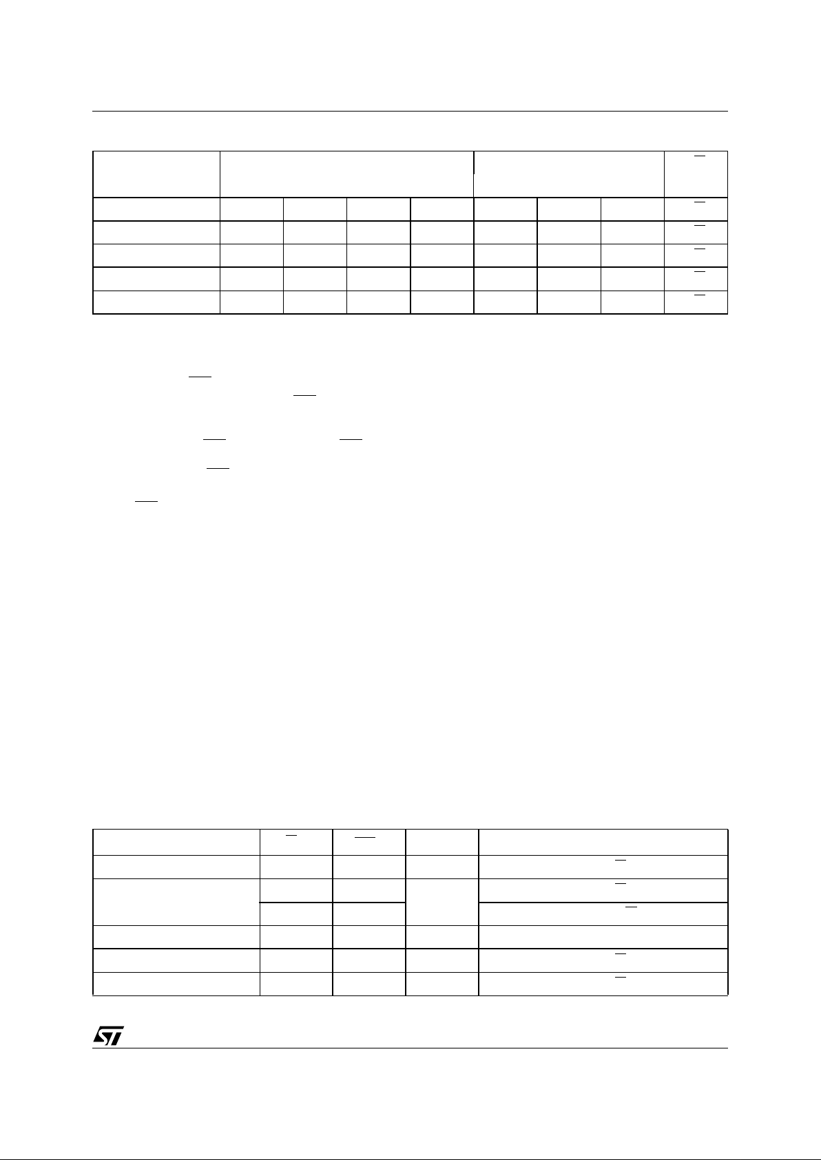
Table 2. Absolute Maximum Ratings
1
Note: 1. Exc ept for the r ating “Oper ating Tempe rature Range”, stresses above th ose listed in the Table “Absolute M aximum Rati ngs” may
cause permanent damage to the device. These are stress ratings only, and operation of the device at these or any other conditions
above those indicated in the Operating sections of this s pecificatio n is not implied. Ex posure to A bsolute Maximum Rating cond i tions for extended periods may affect device reliability. Refer also to the ST SURE Program and other relevant quality documents.
2. MIL -STD-883C , 3015.7 (100 pF, 1500 Ω)
Symbol Parameter Value Unit
T
A
Ambient Operating Temperature -40 to 125 °C
T
STG
Storage
Temperature
-65 to 150 °C
T
LEAD
Lead Temperature
during Soldering
PSDIP8: 10 sec
SO8: 40 sec
TSSOP8: 40 sec
SBGA5: t.b.c.
260
215
215
t.b.c.
°C
V
IO
Input or Output range -0.6 to 6.5 V
V
CC
Supply Voltage -0.3 to 6.5 V
V
ESD
Electrostatic Discharge Voltage (Human Body model2)
4000
V
M24C16, M24C08, M24C04, M24C02, M24C01
4/20
disabled – the device will not respond to any
command. In the same way, when V
CC
drops from
the operating voltage, below the POR threshold
value, all operations are disabled an d the device
will not respond to any command. A stable and
valid V
CC
must be applied before applying any
logic signal.
SIGNAL DESCRIPTION
Serial Clock (SCL)
The SCL input pin is used to strobe all data in and
out of the memory. In applications where this line
is used by slaves to synchronize the bus to a
slower clock, the master must have an open drain
output, and a pull-up resistor must be c onnected
from the SCL line to V
CC
. (Figure 3 indicates how
the value of the pull-up resistor can be calculated).
In most applications, though, this method of
synchronization is not employed, and so the pullup resistor is not necessary, provided that the
master has a push-pull (rather than open drain)
output.
Serial Data (SDA)
The SDA pin is bi-directional, and is used to
transfer data in or out of the memory. It is an open
drain output that may be wire-OR’ed with other
open drain or open collector signals on the bus. A
pull up resistor must be connected f rom the SDA
bus to V
CC
. (Figure 3 indicates how t he value of
the pull-up resistor can be calculated).
Chip Enable (E2, E1, E0)
These chip enable inputs are used to set the value
that is to be looked for on the three least significant
bits (b3, b2, b1) of the 7-bit device select code (but
see the description of memory addressing, on
page 6, for more details). These inputs may be
driven dynamically or tied to V
CC
or VSS to
establish the device select code (but note that the
V
IL
and VIH levels for the inputs are CMOS
compatible, not TTL compatible).
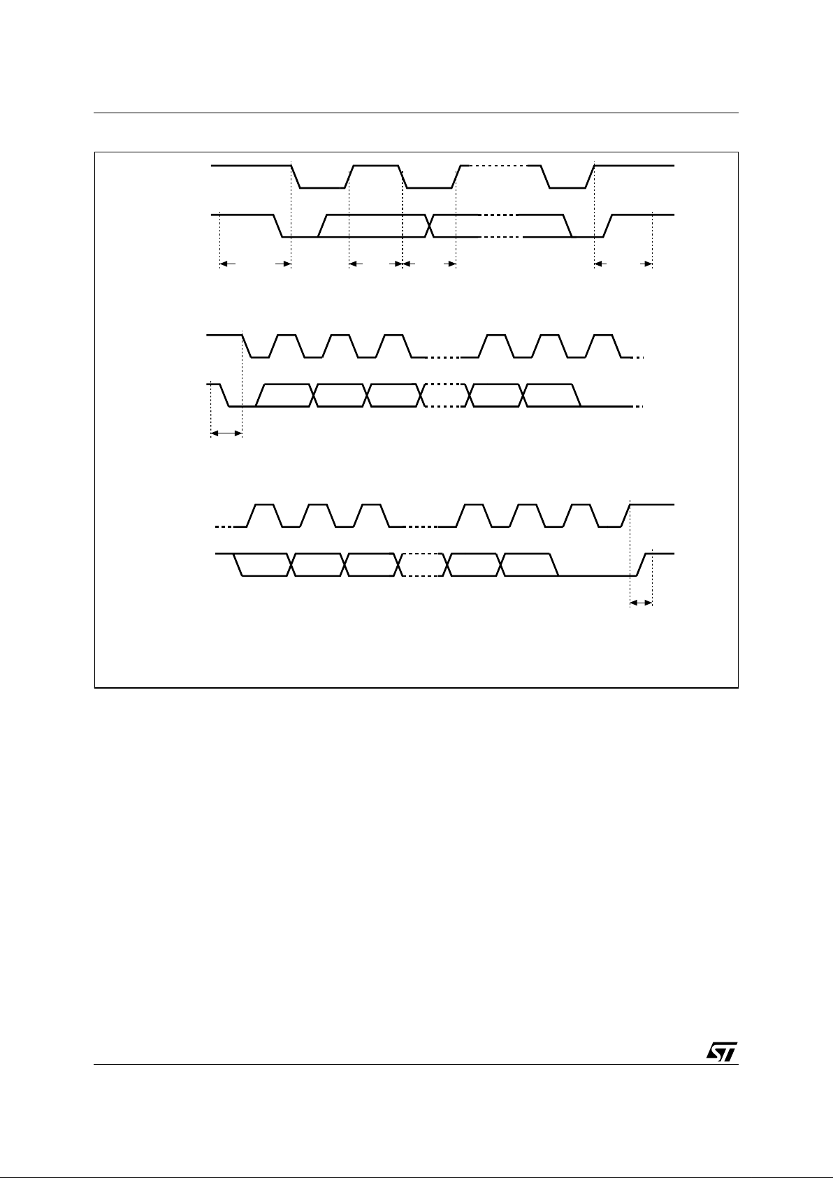
Figure 4. I
2
C Bus Protocol
SCL
SDA
SCL
SDA
SDA
START
CONDITION
SDA
INPUT
SDA
CHANGE
AI00792
STOP
CONDITION
1 23 789
MSB
ACK
START
CONDITION
SCL
1 23 789
MSB ACK
STOP
CONDITION
5/20
M24C16, M24C08, M24C04, M24C 02, M24C01
Write Control (WC)
The hardware Write Control pin (WC
) is useful for
protecting the entire contents of the memory from
inadvertent erase/write. The Write Control signal is
used to enable (WC
=VIL) or disable (WC=VIH)
write instructions to the entire memory area. When
unconnected, the WC
input is internally read as
V
IL
, and write operations are allowed.
When WC
=1, Device Select and Address bytes
are acknowledged, Data bytes are not
acknowledged.
Please see the Application Note
AN404
for a more
detailed description of the Write Control feature.
DEVICE OPERATION
The memory device supports the I
2
C protocol.
This is summarized in Figure 4, and is compared
with other serial bus protocols in Application Note
AN1001
. Any device that sends data on to the bus
is defined to be a transm itter, and any device that
reads the data to be a receiver. The device that
controls the data transfer is k nown as the master,
and the other as the slave. A data transfer can only
be initiated by the mas ter, which wi ll also provide
the serial clock for synchronization. The memory
device is always a slave device in all
communication.
Start Condition
START is identified by a high t o low transition of
the SDA line while the clock, SCL, is stab le in t he
high state. A START condition must precede any
data transfer command. The memory device
continuously monitors (except during a
programming cycle) the SDA and SCL lines for a
START condition, and will not respond unless one
is given.
Stop Condition
STOP is identified by a low to high transition of the
SDA line wh ile th e clock S CL is sta ble in the h igh
state. A STOP condition terminates
communication between the m emory device and
the bus master. A STOP condition at the end of a
Read command, after (and only after) a NoAck,
forces the memory device into its standby state. A
STOP condition at the end of a Write com mand
triggers the internal EEPROM write cycle.
Acknowledge Bit (ACK)
An acknowledge signal is used to indicate a
successful byte transfer. The bus transmitter,
whether it be master or slave, releases the SDA
bus after sending eight bits of data. During the 9
th
Table 3. Device Select Code
1
Note: 1. The most significant bit, b7, is sent first.
2. E0, E1 and E2 are comp ared against the respective ext ernal pins on the memory device.
3. A10, A9 and A8 repres ent high significant bits of the address.
Device Type Identifier Chip Enable RW
b7 b6 b5 b4 b3 b2 b1 b0
M24C01 Select Code 1010E2E1E0RW
M24C02 Select Code 1010E2E1E0RW
M24C04 Select Code 1010E2E1A8RW
M24C08 Select Code 1010E2A9A8RW
M24C16 Select Code 1010A10A9A8RW
Table 4. Operating Modes
Note: 1. X = V
IH
or V
IL
.
Mode RW bit
WC
1
Bytes Initial Sequence
Current Address Read 1 X 1 START, Device Select, RW
= ‘1’
Random Address Read
0X
1
START, Device Select, RW
= ‘0’, Address
1 X reSTART, Device Select, RW
= ‘1’
Sequential Read 1 X
≥
1 Similar to Current or Random Address Read
Byte Write 0 V
IL
1 START, Device Select, RW = ‘0’
Page Write 0 V
IL
≤
16 START, Device Select, RW
= ‘0’
M24C16, M24C08, M24C04, M24C02, M24C01
6/20
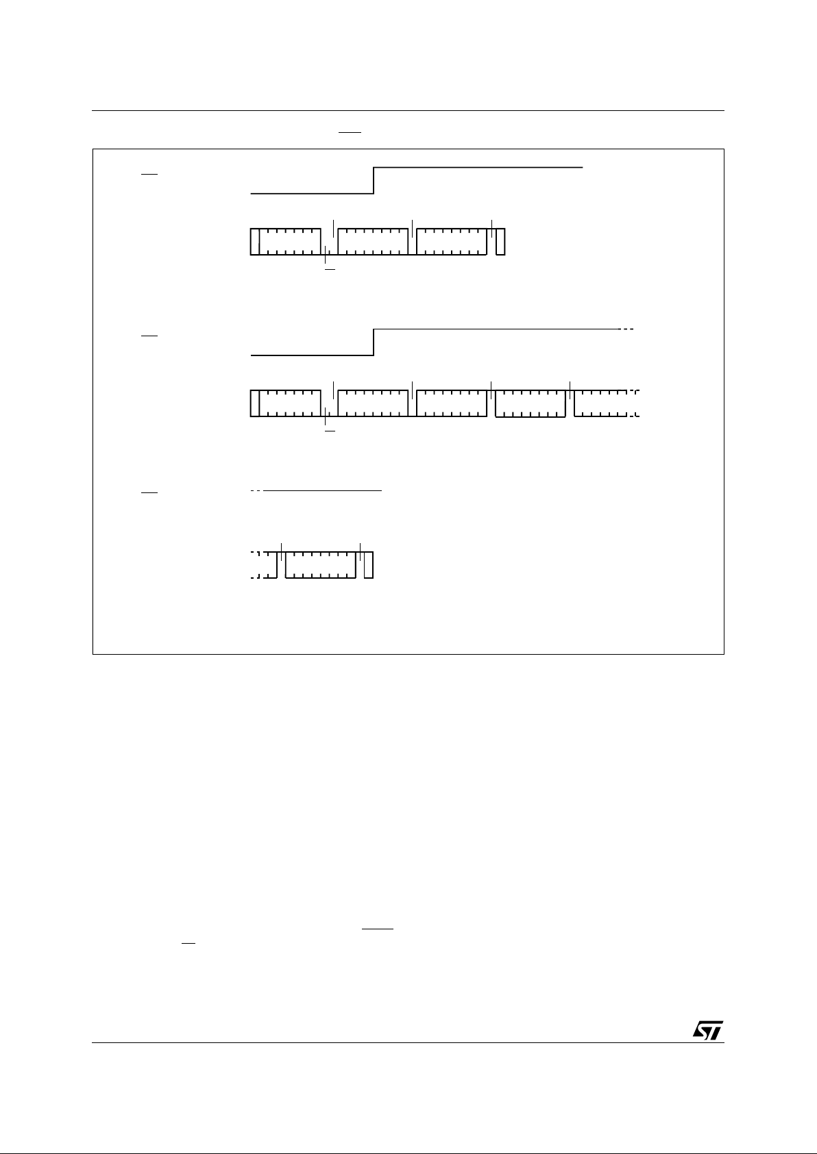
Figure 5. Wri te Mo de S e qu e nces with WC=1 (data wri te inhibi ted)
STOP
START
BYTE WRITE DEV SEL BYTE ADDR DATA IN
WC
START
PAGE WRITE DEV SEL BYTE ADDR DATA IN 1 DATA IN 2
WC
DATA IN 3
AI02803B
PAGE WRITE
(cont'd)
WC (cont'd)
STOP
DATA IN N
ACK ACK NO ACK
R/W
ACK ACK NO ACK NO ACK
R/W
NO ACK NO ACK
clock pulse period, the receiver pulls the SDA bus
low to acknowledge the receipt of the eight data
bits.
Data Input
During data input, the memory device samples the
SDA bus signal on the rising edge of the clock,
SCL. For correct device operation, the SDA signal
must be stable during the clock low-to-high
transition, and the data must change
only
when
the SCL line is low .
Memory Addressing
To start communication betwee n the bus master
and the slave memory, the master must initiate a
START condition. Following this, the master sends
the 8-bit byte, shown in Table 3, on the SDA bus
line (most significant bit first). This consists of the
7-bit Device Select Code, and the 1-bit Read/Write
Designator (RW). The Device Select Code is
further subdivided into: a 4-bit Device Type
Identifier, and a 3-bit Chip Enable “Address” (E2,
E1, E0 ) .
To address the memory array, the 4-bit Device
Type Identifier is 1010b.
Up to eight memory devices can be connected on
a single I
2
C bus. Each one is given a uniq ue 3-bit
code on its Chip Enable inputs. W hen the Device
Select Code is received, the memory only
responds if the Chip Enable Code (shown in Table
3) is the same as the pattern applied to its Chip
Enable pins.
Those devices with larger memory capacities (the
M24C16, M24C08 and M24C04) need more
address bits. E0 is not available for use on devices
that need to use address line A8; E1 is not
available for devices that need to use address line
A9, and E2 is not available for devices that need to
use address line A10 (see Figure 2A to Figure 2D
and Table 3 for details). Using the E0, E1 and E2
inputs pins, up to eight M24C02 (or M24C01), four
M24C04, two M24C08 or one M24C16 device can
be connected to one I
2
C bus. In each case, and in
the hybrid cases, this gives a total memory
 Loading...